 | –≠–ª–µ–∫—Ç—Ä–æ–Ω–Ω—ã–π –∫–æ–º–ø–æ–Ω–µ–Ω—Ç: TDA2653A | –°–∫–∞—á–∞—Ç—å:  PDF PDF  ZIP ZIP |

DATA SHEET
Product specification
File under Integrated Circuits, IC02
January 1991
INTEGRATED CIRCUITS
TDA2653A
Vertical deflection circuit

January 1991
2
Philips Semiconductors
Product specification
Vertical deflection circuit
TDA2653A
DESCRIPTION
The TDA2653A is a monolithic integrated circuit for vertical deflection in large screen colour television receivers.
The circuit incorporates the following functions:
∑
Oscillator; switch capability for 50 Hz/60 Hz operation
∑
Synchronization circuit
∑
Blanking pulse generator with guard circuit
∑
Sawtooth generator with buffer stage
∑
Preamplifier with fed-out inputs
∑
Output stage with thermal and short-circuit protection
∑
Flyback generator
∑
Voltage stabilizers
QUICK REFERENCE DATA
Note
1. for 45 AX systems
PACKAGE OUTLINE
13-lead SIL; plastic power (SOT141RGA); SOT141-6; 1996 November 19.
Supply voltage (pin 9)
V
9-8
= V
S
typ.
26 V
Supply current (pin 5
+
pin 9)
(1)
I
5
+
I
9
= I
S
typ.
325 mA
Output current (peak-to-peak value)
(1)
I
6(p-p)
typ.
1,7 A
Maximum output current (peak-to-peak value)
I
6(p-p)
max.
2,6 A
Picture frequency
f
50 Hz/60 Hz
Sync input pulse (peak-to-peak value)
V
2-8(p-p)
1 V
Thermal resistance from junction to mounting base
R
th j-mb
5 K/W
January 1991
3
Philips Semiconductors
Product specification
Vertical deflection circuit
TDA2653A
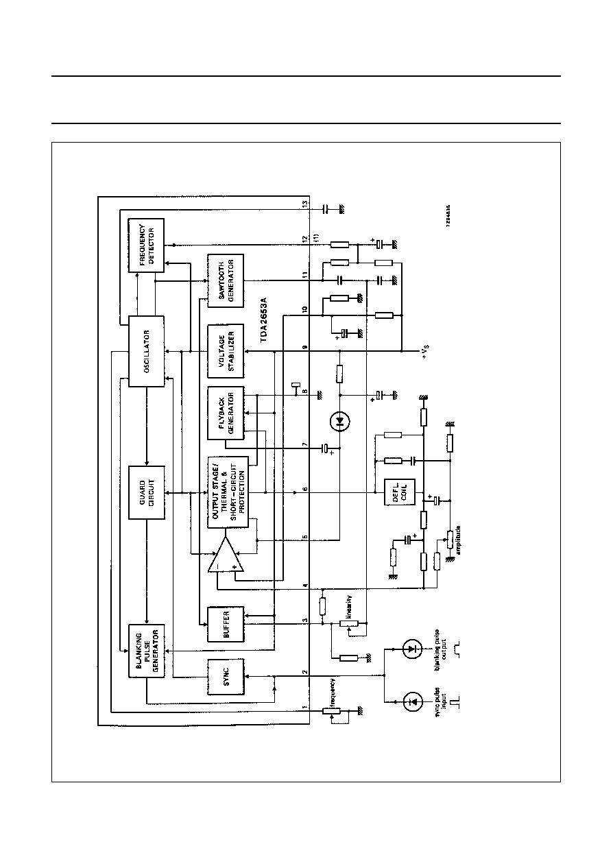
Fig.1 Block diagram.
(1) Condition for pin 12: LOW voltage level = 50 Hz; HIGH voltage level = 60 Hz.
January 1991
4
Philips Semiconductors
Product specification
Vertical deflection circuit
TDA2653A
RATINGS
Limiting values in accordance with the Absolute Maximum System (IEC 134)
Supply voltage (pin 9)
V
9
-
8
= V
S
max.
40
V
Supply voltage output stage (pin 5)
V
5-8
max.
60
V
Voltages
Pin 3
V
3
-
11
max.
7
V
Pin 13
V
13-8
max.
7
V
Pins 4 and 10
V
4; 10-8
max.
24
V
Pin 6
v
6-8
max.
60
V
-
V
6
-
8
max.
0
V
Pins 7 and 11
V
7; 11
-
8
max.
40
V
Currents
Pin 1
I
1
max.
0
mA
-
I
1
max.
1
mA
Pin 2
±
I
2
max.
10
mA
Pin 3
I
3
max.
0
mA
-
I
3
max.
5
mA
Pin 7
I
7
max.
1,3
A
-
I
7
max.
1,5
A
Pin 11
I
11
max.
50
mA
-
I
11
max.
1
mA
Pin 12
I
12
max.
3
mA
-
I
12
max.
0
mA
Pins 5, 6 and 8: internally limited by the short-circuit protection circuit.
Total power dissipation: internally limited by the thermal protection circuit.
Storage temperature range
T
stg
-
25 to
+
150
∞
C
Operating ambient temperature range
T
amb
0
∞
C to limiting value
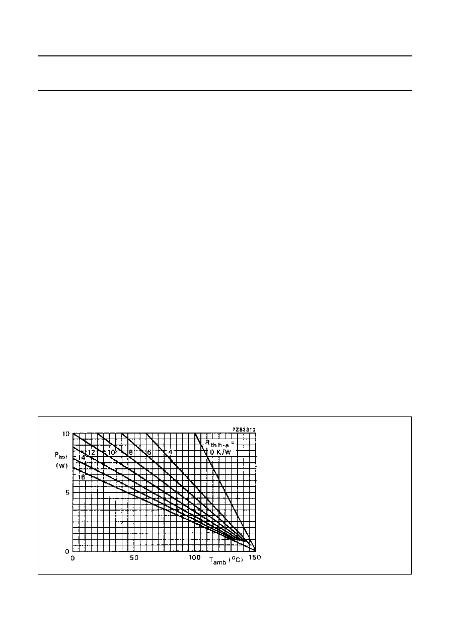
Fig.2
Total power dissipation.
R
th h-a
includes R
th mb-h
which is expected when heat-
sink compound is used.
R
th j
-
mb
5 K/W.

January 1991
5
Philips Semiconductors
Product specification
Vertical deflection circuit
TDA2653A
CHARACTERISTICS
T
amb
= 25
∞
C unless otherwise specified.
Supply voltage/output stage
Supply voltage
V
9-8
= V
S
9 to 30
V
Output voltage
at
-
I
6
= 1,1 A
V
6-8
V
5-8
-
2,2
V
typ.
V
5-8
-
1,9
V
at I
6
= 1,1 A
V
6-8
typ.
1,3
V
1,6
V
Flyback generator output voltage at
-
I
7
= 1,1 A
V
7-8
typ.
V
S
-
2,2
V
Peak output current
±
I
6
1,3
A
Flyback generator peak current
±
I
7
1,3
A
Feedback
Input quiescent current
-
I
4; 10
typ.
0,1
µ
A
Synchronization
Sync input pulse
V
2-8
1 to 12
V
Tracking range
typ.
28
%
Oscillator/sawtooth generator
Oscillator frequency control input voltage
V
1-8
6 to 9
V
Sawtooth generator output voltage
V
3-8
0 to V
S
-
1
V
V
11-8
0 to V
S
-
2
V
Sawtooth generator output current
-
I
3
0 to 4
mA
I
11
-
2
µ
A
+
30
mA
Oscillator temperature dependency
T
case
= 20 to 100
∞
C
(
f/f)/
T
case
typ.
10
-4
K
-1
Oscillator voltage dependency
V
S
= 10 to 30 V
(
f/f)/
V
S
typ.
4 x 10
-4
V
-1
Blanking pulse generator
Output voltage
at V
S
= 24 V; I
2
= 1 mA
V
2
-
8
typ.
18,5
V
Output current
-
I
2
3
mA
Output resistance
R
2
-
8
typ.
410
Blanking pulse duration at 50 Hz sync
t
b
typ.
1,4
±
0,07
ms
50 Hz/60 Hz switch capability
Saturation voltage; LOW voltage level
V
12
-
8
typ.
1
V
Output leakage current
I
12
typ.
1
µ
A
Thermal resistance/junction temperature
From junction to mounting base
R
th j-mb
5
K/W
Junction temperature; switching point thermal protection
T
j
typ.
150
±
8
∞
C

January 1991
6
Philips Semiconductors
Product specification
Vertical deflection circuit
TDA2653A
PINNING
1. Oscillator adjustment
2. Synchronization input/blanking output
3. Sawtooth generator output
4. Preamplifier input
5. Positive supply of output stage
6. Output
7. Flyback generator output
8. Ground
9. Positive supply (V
S
)
10. Reference voltage
11. Sawtooth capacitor
12. 50 Hz/ 60 Hz switching voltage
13. Oscillator capacitor

January 1991
7
Philips Semiconductors
Product specification
Vertical deflection circuit
TDA2653A
APPLICATION INFORMATION
The function is described against the corresponding pin number
1, 13.
Oscillator
The oscillator frequency is determined by a potentiometer at pin 1 and a capacitor at pin 13.
2.
Sync input/blanking output
Combination of sync input and blanking output. The oscillator has to be synchronized by a positive-going
pulse between 1 and 12 V. The integrated frequency detector delivers a switching level at pin 12.
The blanking pulse amplitude is 20 V with a load of 1 mA.
3.
Sawtooth generator output
The sawtooth signal is fed via a buffer stage to pin 3. It delivers the signal which is used for linearity control,
and drive of the preamplifier. The sawtooth is applied via a shaping network to pin 11 (linearity) and via a
resistor to pin 4 (preamplifier).
4.
Preamplifier input
The DC voltage is proportional to the output voltage (DC feedback). The AC voltage is proportional to the
sum of the buffered sawtooth voltage at pin 3 and the voltage, with opposite polarity, at the feedback
resistor (AC feedback).
5.
Positive supply of output stage
This supply is obtained from the flyback generator. An electrolytic capacitor between pins 7 and 5, and a
diode between pins 5 and 9 have to be connected for proper operation of the flyback generator.
6.
Output of class-B power stage
The vertical deflection coil is connected to this pin, via a series connection of a coupling capacitor and a
feedback resistor, to ground.
7.
Flyback generator output
An electrolytic capacitor has to be connected between pins 7 and 5 to complete the flyback generator.
8.
Negative supply (ground)
Negative supply of output stage and small signal part.
9.
Positive supply
The supply voltage at this pin is used to supply the flyback generator, voltage stabilizer, blanking pulse
generator and buffer stage.
10.
Reference voltage of preamplifier
External adjustment and decoupling of reference voltage of the preamplifier.
11.
Sawtooth capacitor
This sawtooth capacitor has been split to realize linearity control.
12.
50 Hz/60 Hz switching level
This pin delivers a LOW voltage level for 50 Hz and a HIGH voltage level for 60 Hz. The amplitudes of the
sawtooth signals can be made equal for 50 Hz and 60 Hz with these levels.
January 1991
8
Philips Semiconductors
Product specification
Vertical deflection circuit
TDA2653A
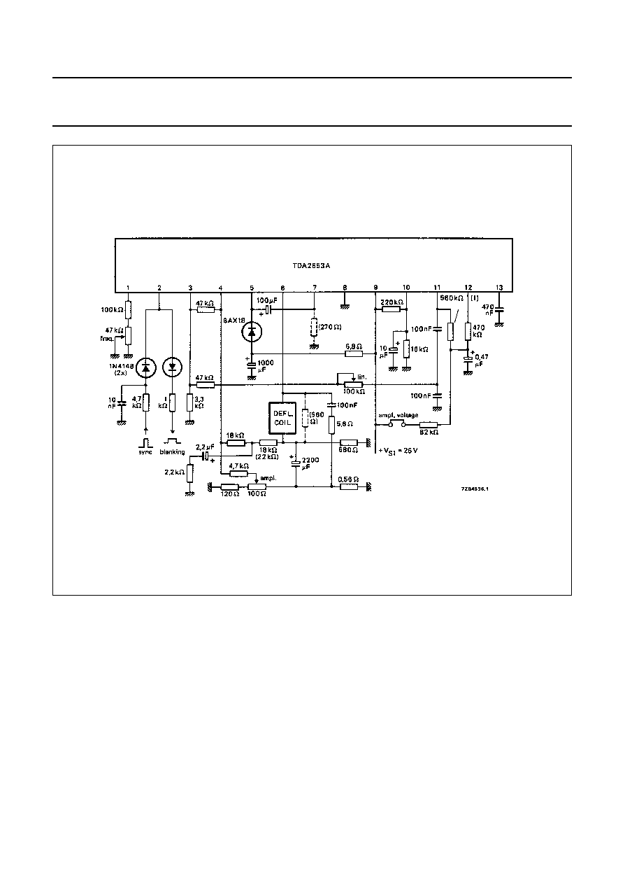
Fig.3 Typical vertical deflection circuit for 45AX system (26 V).
(1) Condition for pin 12: LOW voltage level = 50 Hz; HIGH voltage level = 60 Hz.

January 1991
9
Philips Semiconductors
Product specification
Vertical deflection circuit
TDA2653A
Fig.4 Typical vertical deflection circuit for 45 AX system (V
S1
= 26 V, V
S2
= 12 V) in quasi-bridge connection.
(1) Condition for pin 12: LOW voltage level = 50 Hz; HIGH voltage level = 60 Hz.

January 1991
10
Philips Semiconductors
Product specification
Vertical deflection circuit
TDA2653A
PACKAGE OUTLINE
UNIT
A
e
1
A
2
b
p
c
D
(1)
E
(1)
Z
(1)
d
e
D
h
L
L
3
m
REFERENCES
OUTLINE
VERSION
EUROPEAN
PROJECTION
ISSUE DATE
IEC
JEDEC
EIAJ
mm
17.0
15.5
4.6
4.2
0.75
0.60
0.48
0.38
24.0
23.6
20.0
19.6
10
3.4
v
0.8
12.2
11.8
1.7
e
2
5.08
2.4
1.6
E
h
6
2.00
1.45
2.1
1.8
3.4
3.1
4.3
DIMENSIONS (mm are the original dimensions)
Note
1. Plastic or metal protrusions of 0.25 mm maximum per side are not included.
12.4
11.0
SOT141-6
0
5
10 mm
scale
Q
j
0.25
w
0.03
x
D
L
E
A
c
A
2
m
L
3
Q
w
M
b
p
1
d
D
Z
e
2
e
e
x
h
1
13
j
Eh
non-concave
view B: mounting base side
92-11-17
95-03-11
DBS13P: plastic DIL-bent-SIL power package; 13 leads (lead length 12 mm)
SOT141-6
v
M
B

January 1991
11
Philips Semiconductors
Product specification
Vertical deflection circuit
TDA2653A
SOLDERING
Introduction
There is no soldering method that is ideal for all IC packages. Wave soldering is often preferred when through-hole and
surface mounted components are mixed on one printed-circuit board. However, wave soldering is not always suitable for
surface mounted ICs, or for printed-circuits with high population densities. In these situations reflow soldering is often
used.
This text gives a very brief insight to a complex technology. A more in-depth account of soldering ICs can be found in our
"IC Package Databook" (order code 9398 652 90011).
Soldering by dipping or by wave
The maximum permissible temperature of the solder is 260
∞
C; solder at this temperature must not be in contact with the
joint for more than 5 seconds. The total contact time of successive solder waves must not exceed 5 seconds.
The device may be mounted up to the seating plane, but the temperature of the plastic body must not exceed the
specified maximum storage temperature (T
stg max
). If the printed-circuit board has been pre-heated, forced cooling may
be necessary immediately after soldering to keep the temperature within the permissible limit.
Repairing soldered joints
Apply a low voltage soldering iron (less than 24 V) to the lead(s) of the package, below the seating plane or not more
than 2 mm above it. If the temperature of the soldering iron bit is less than 300
∞
C it may remain in contact for up to
10 seconds. If the bit temperature is between 300 and 400
∞
C, contact may be up to 5 seconds.
DEFINITIONS
LIFE SUPPORT APPLICATIONS
These products are not designed for use in life support appliances, devices, or systems where malfunction of these
products can reasonably be expected to result in personal injury. Philips customers using or selling these products for
use in such applications do so at their own risk and agree to fully indemnify Philips for any damages resulting from such
improper use or sale.
Data sheet status
Objective specification
This data sheet contains target or goal specifications for product development.
Preliminary specification
This data sheet contains preliminary data; supplementary data may be published later.
Product specification
This data sheet contains final product specifications.
Limiting values
Limiting values given are in accordance with the Absolute Maximum Rating System (IEC 134). Stress above one or
more of the limiting values may cause permanent damage to the device. These are stress ratings only and operation
of the device at these or at any other conditions above those given in the Characteristics sections of the specification
is not implied. Exposure to limiting values for extended periods may affect device reliability.
Application information
Where application information is given, it is advisory and does not form part of the specification.