Document Outline
- FEATURES
- PROTECTIONS
- GENERAL DESCRIPTION
- QUICK REFERENCE DATA
- ORDERING INFORMATION
- BLOCK DIAGRAM
- PINNING
- FUNCTIONAL DESCRIPTION
- LIMITING VALUES
- THERMAL CHARACTERISTICS
- QUALITY SPECIFICATION
- CHARACTERISTICS
- TEST AND APPLICATION INFORMATION
- Test information
- Application information
- PACKAGE OUTLINE
- SOLDERING
- DEFINITIONS
- LIFE SUPPORT APPLICATIONS

DATA SHEET
Product specification
Supersedes data of 1997 Aug 12
File under Integrated Circuits, IC01
1998 May 07
INTEGRATED CIRCUITS
TDA3606A
Multiple voltage regulator with
battery detection

1998 May 07
2
Philips Semiconductors
Product specification
Multiple voltage regulator with battery
detection
TDA3606A
FEATURES
∑
One V
P
-state controlled regulator
∑
Regulator and reset outputs operate during load dump
∑
Supply voltage range of
-
18 to +50 V
∑
Low quiescent current (battery detection switched off)
∑
High ripple rejection
∑
Dual reset output.
PROTECTIONS
∑
Reverse polarity safe (down to
-
18 V without high
reverse current)
∑
Able to withstand voltages up to 18 V at the output
(supply line may be short-circuited)
∑
ESD protected on all pins
∑
Load dump protection
∑
Foldback current limit protection for regulator
∑
DC short-circuit safe to ground and V
P
of regulator
output.
GENERAL DESCRIPTION
The TDA3606A is a low power voltage regulator.
It contains:
1. One fixed voltage regulator with a foldback current
protection, intended to supply a microprocessor, that
also operates during load dump
2. A reset-signal can be used to interface with the
microprocessor
3. Supply pin can withstand load dump pulses and
negative supply voltages
4. Defined start-up behaviour; regulator will be switched
on at a supply voltage higher than 7.6 V and off when
the output voltage of the regulator drops below 2.4 V.
QUICK REFERENCE DATA
ORDERING INFORMATION
SYMBOL
PARAMETER
CONDITIONS
MIN.
TYP.
MAX.
UNIT
Supplies
V
P
supply voltage
operating
regulator on
5.6
14.4
25
V
jump start
t
10 minutes
-
-
30
V
load dump protection
t
50 ms; t
r
2.5 ms
-
-
50
V
I
q(tot)
total quiescent supply current
standby mode
-
95
120
µ
A
Voltage regulator
V
REG
output voltage regulator
7 V
V
P
18 V
4.85
5.0
5.15
V
0.5 mA
I
REG
150 mA
4.8
5.0
5.2
V
V
REGd
drop-out voltage
I
REG
= 150 mA
-
-
0.5
V
TYPE
NUMBER
PACKAGE
NAME
DESCRIPTION
VERSION
TDA3606AT
SO20
plastic small outline package; 20 leads; body width 7.5 mm
SOT163-1

1998 May 07
3
Philips Semiconductors
Product specification
Multiple voltage regulator with battery
detection
TDA3606A
BLOCK DIAGRAM
Fig.1 Block diagram.
handbook, full pagewidth
MGK597
REGULATOR
LOAD DUMP
PROTECTION
REFERENCE
7
&
GND
1 to 3, 8 to 13, 18 to 20
n.c.
TDA3606A
REG
REG
RES2
RES1
(14.4 V)
(5 V/150 mA)
14
16
BATTERY
BUFFER
VO(bat)
VI(bat)
VC
VP
15
5
4
6
17
4.7
k
4.7
k
PINNING
SYMBOL
PIN
DESCRIPTION
n.c.
1 to 3
not connected; heat spreader
V
I(bat)
4
battery input voltage
V
O(bat)
5
battery detection output voltage
V
C
6
reset delay capacitor
GND
7
ground (0 V)
n.c.
8 to 13
not connected; heat spreader
RES2
14
reset 2 output
RES1
15
reset 1 output
REG
16
regulator output
V
P
17
supply voltage
n.c.
18 to 20
not connected; heat spreader
Fig.2 Pin configuration.
handbook, halfpage
n.c.
n.c.
n.c.
VI(bat)
VO(bat)
VC
GND
n.c.
n.c.
n.c.
n.c.
n.c.
n.c.
VP
RES1
RES2
REG
n.c.
n.c.
n.c.
1
2
3
4
5
6
7
8
9
10
11
12
20
19
18
17
16
15
14
13
TDA3606AT
MGK600
1998 May 07
4
Philips Semiconductors
Product specification
Multiple voltage regulator with battery
detection
TDA3606A
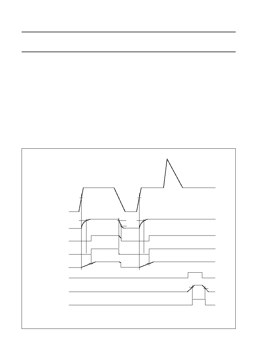
FUNCTIONAL DESCRIPTION
The TDA3606A is a voltage regulator intended to supply a
microprocessor (e.g. in car radio applications). Because of
low voltage operation of the application, a low-voltage drop
regulator is used in the TDA3606A.
This regulator will switch on when the supply voltage
exceeds 7.6 V for the first time and will switch off again
when the output voltage of the regulator drops below
2.4 V. When the regulator is switched on, the RES1 and
RES2 outputs (RES2 can only be HIGH when RES1 is
HIGH) will go HIGH after a fixed delay time (fixed by an
external delay capacitor) to generate a reset to the
microprocessor.
RES1 will go HIGH by an internal pull-up resistor of 4.7 k
,
and is used to initialize the microprocessor. RES2 is used
to indicate that the regulator output voltage is within its
voltage range. This start-up feature is built-in to secure a
smooth start-up of the microprocessor at first connection,
without uncontrolled switching of the regulator during the
start-up sequence.
All output pins are fully protected. The regulator is
protected against load dump and short-circuit (foldback
current protection).
Interfacing with the microprocessor can be accomplished
by means of a battery Schmitt-trigger and output buffer
(simple full/semi on/off logic applications). The battery
output will go HIGH when the battery input voltage
exceeds the HIGH threshold level.
Fig.3 Timing diagrams.
handbook, full pagewidth
2.1 V
VP
regulator
reset 1
50 V
4.35 V
4.35 V
2.4 V
2 V
2 V
2 V
reset 2
on/off switch
battery input
battery output
reset delay
capacitor
MGB857

1998 May 07
5
Philips Semiconductors
Product specification
Multiple voltage regulator with battery
detection
TDA3606A
LIMITING VALUES
In accordance with the Absolute Maximum Rating System (IEC 134).
THERMAL CHARACTERISTICS
Notes
1. On IMS board.
2. On standard board with double sided copper area connected to pins.
QUALITY SPECIFICATION
In accordance with
"SNW-FQ-611E". The number of the quality specification can be found in the "Quality Reference
Handbook". The handbook can be ordered using the code 9397 750 00192.
SYMBOL
PARAMETER
CONDITIONS
MIN.
MAX.
UNIT
V
P
supply voltage
operating
regulator on
-
25
V
jump start
t
10 minutes
-
30
V
load dump protection
t
50 ms; t
r
2.5 ms
-
50
V
V
P
reverse battery voltage
non-operating
-
-
18
V
V
I(bat)p
positive pulse voltage at battery input
V
P
= 14.4 V; R
I
= 5 k
-
50
V
V
I(bat)n
negative pulse voltage at battery input
V
P
= 14.4 V; R
I
= 5 k
-
-
100
V
P
tot
total power dissipation
T
amb
= 25
∞
C
-
2.5
W
T
stg
storage temperature
non-operating
-
55
+150
∞
C
T
amb
operating ambient temperature
-
40
+85
∞
C
T
j
junction temperature
operating
-
40
+150
∞
C
SYMBOL
PARAMETER
CONDITIONS
VALUE
UNIT
R
th (j-p)
thermal resistance from junction to pins
20
K/W
R
th (j-a)
thermal resistance from junction to
ambient
in free air; note 1
50
K/W
in free air; note 2
60
K/W

1998 May 07
6
Philips Semiconductors
Product specification
Multiple voltage regulator with battery
detection
TDA3606A
CHARACTERISTICS
V
P
= 14.4 V; T
amb
= 25
∞
C; see Fig.5; unless otherwise specified.
SYMBOL
PARAMETER
CONDITIONS
MIN.
TYP.
MAX.
UNIT
Supplies
V
P
supply voltage
operating
regulator on; note 1
5.6
14.4
25
V
jump start
t
10 minutes
-
-
30
V
load dump protection
t
50 ms, t
r
2.5 ms
-
-
50
V
I
q
quiescent current
V
P
= 12.4 V; note 2
-
95
120
µ
A
V
P
= 14.4 V; note 2
-
100
-
µ
A
load dump; V
P
= 50 V
-
5
20
mA
Schmitt-trigger for regulator and reset 1
V
thr
rising supply voltage threshold
6.2
7.5
8.2
V
V
thf
falling voltage of regulator
threshold
I
REG
= 5 mA
2.1
2.4
2.7
V
I
REG
= 30 mA
-
2.25
-
V
V
hys
hysteresis
-
5.1
-
V
Schmitt-trigger for battery detection
V
thr
rising voltage threshold
1.9
2.05
2.2
V
V
thf
falling voltage threshold
1.8
1.95
2.1
V
V
hys
hysteresis
-
0.1
-
V
Schmitt-trigger for reset 2
V
thr
rising voltage of regulator
note 3
4.25
4.45
4.65
V
V
thf
falling voltage of regulator
note 3
4.15
4.35
4.55
V
V
hys
hysteresis
-
0.1
-
V
Reset 1 and reset 2 buffers
I
sink
LOW-level sink current
V
RES
0.8 V; note 3
2
-
-
mA
R
pu
internal pull-up resistor
3.7
4.7
5.7
k
Reset delay
I
o
output current
-
0.75
-
µ
A
V
thr
rising voltage threshold
1.4
2.0
2.8
V
t
d
delay time
C
d
= 47 nF; note 4
40
125
-
ms
Battery buffer
V
OL
LOW-level output voltage
I
I
= 0 mA
0
0.05
0.8
V
V
OH
HIGH-level output voltage
I
o
= 5
µ
A; note 5
-
5.0
5.2
V
I
OL
LOW-level output current
V
OL
0.8 V
0.2
0.5
-
mA
I
OH
HIGH-level output current
V
OH
3 V
0.3
1.0
-
mA

1998 May 07
7
Philips Semiconductors
Product specification
Multiple voltage regulator with battery
detection
TDA3606A
Notes
1. Minimum operating voltage, only if V
P
has exceeded 7.6 V.
2. The quiescent current is measured in standby mode. So, the battery input is connected to a low voltage source and
R
L
=
.
3. The voltage of regulator sinks as a result of a supply voltage drop.
4. The delay time can be calculated with the following formula:
5. Battery output voltage will be equal or less than the output voltage of regulator.
6. The drop-out voltage of regulator is measured between V
P
and V
REG
.
7. At current limit, I
clr
is held constant (behaviour according to dashed line in Fig.4).
8. The foldback current protection limits the dissipated power at short-circuit (see Fig.4).
Regulator (I
REG
= 5 mA)
V
o
output voltage
0.5 mA
I
REG
150 mA;
7 V
V
P
18 V
4.8
5.0
5.2
V
18 V
V
P
50 V; load dump;
I
REG
= 30 mA
4.75
5.0
5.25
V
I
o
output current
load dump; V
P
> 25 V
-
-
100
mA
V
REG
line regulation
7 V
V
P
18 V
-
3
50
mV
V
REGL
load regulation
0.5 mA
I
REG
150 mA
-
-
70
mV
SVRR
supply voltage ripple rejection
f
i
= 200 Hz; V
i(p-p)
= 2 V;
I
o
= 5 mA
55
60
-
dB
V
REGd
drop-out voltage
I
REG
= 150 mA; V
P
= 5.5 V;
note 6
-
0.9
1
V
I
clr
current limit
V
REG
> 4.5 V; note 7
0.2
0.27
0.6
A
I
scr
short-circuit current
R
L
0.5
; note 8
50
80
-
mA
SYMBOL
PARAMETER
CONDITIONS
MIN.
TYP.
MAX.
UNIT
t
d
C
d
I
ch
------- dV
thr
C
d
V
thr
◊
I
ch
----------------------- (ms)
=
=
Fig.4 Foldback current protection.
handbook, halfpage
50 mA
MGB853
5.0 V
1 V
VREG
Iscr
IREG
Iclr
1998 May 07
8
Philips Semiconductors
Product specification
Multiple voltage regulator with battery
detection
TDA3606A
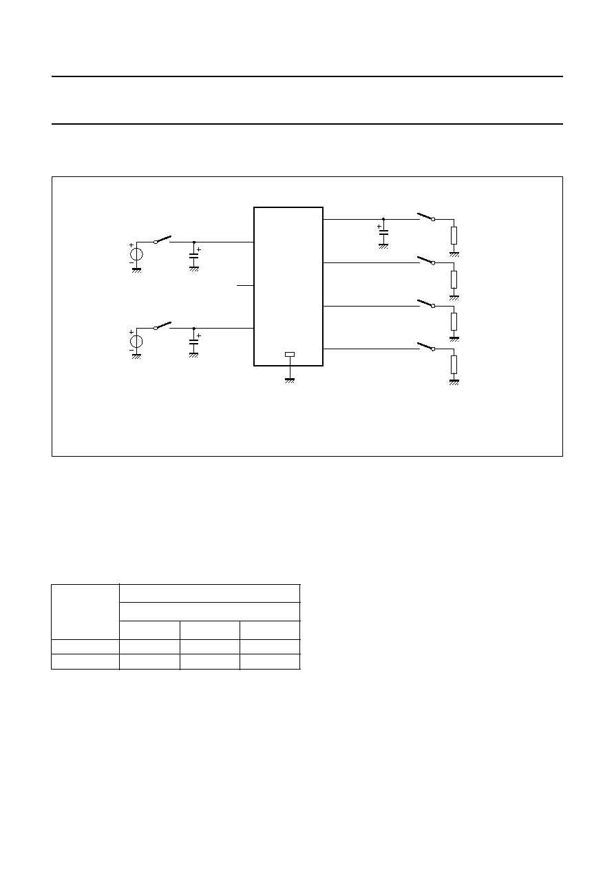
TEST AND APPLICATION INFORMATION
Test information
Fig.5 Test circuit.
(1) Capacitor not required for stability.
handbook, full pagewidth
MGK598
reset 1 output
reset 2 output
1 k
battery output voltage
RL(RES1)
1 k
RL(RES2)
1 k
RL(bat)
15
16
14
5
6
17
7
TDA3606A
GND
VP
VP
VC
battery input voltage
4
VI(bat)
(1)
regulator output
10
µ
F
10
µ
F
10
µ
F
1 k
.. 0.5
RL(REG)
Application information
N
OISE
The noise at the output of the regulator depends on the
bandwidth of the regulator, which can be adjusted by
means of the output capacitor. In Table 1 the noise figures
are given.
Table 1
Noise figures
Note
1. Measured at a bandwidth of 10 Hz to 100 kHz.
The noise on the supply line depends on the value of the
supply capacitor and is caused by a current noise (output
noise of the regulator is translated into a current noise by
means of the output capacitor). When a high frequency
capacitor of 220 nF in parallel with an electrolytic capacitor
OUTPUT
CURRENT
I
O
(mA)
NOISE FIGURE (
µ
V)
(1)
AT OUTPUT CAPACITOR C
L
(
µ
F)
10
47
100
0.5
58
50
45
50
250
200
180
of 100
µ
F is connected directly to pins 17 and 7 (supply
and ground) the noise is minimized.
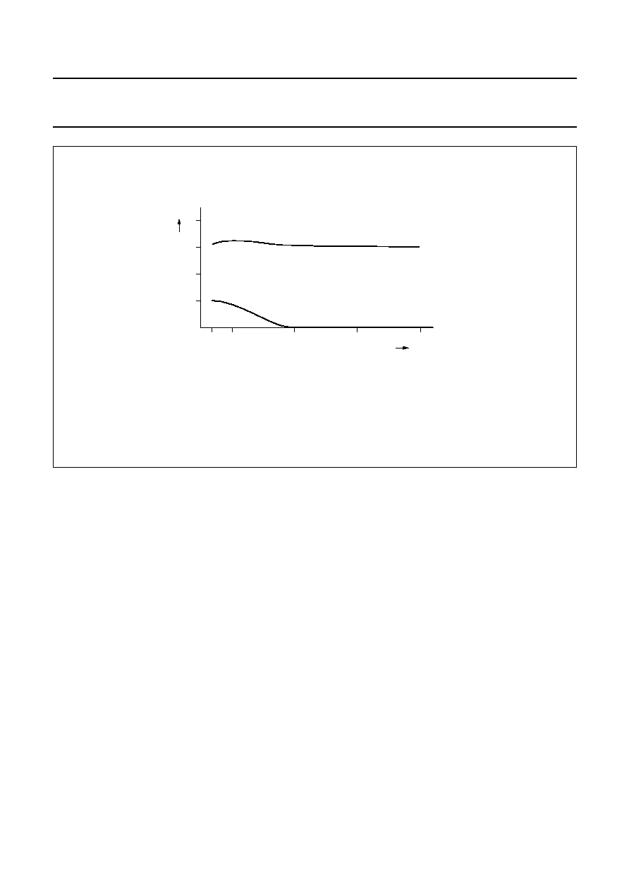
S
TABILITY
The regulator is stabilized by means of the output
capacitor. The value of the output capacitor can be
selected using the diagram shown in Fig.6. The following
two examples show the effects of the stabilization circuit
using different values for the output capacitor.
Example 1
The regulator is stabilized using an electrolytic output
capacitor of 68
µ
F (ESR = 0.5
). At
-
40
∞
C the capacitor
value is decreased to 22
µ
F and the ESR is increased to
3.5
. The regulator will remain stable at a temperature of
-
40
∞
C.
Example 2
The regulator is stabilized using an electrolytic output
capacitor of 10
µ
F (ESR = 3.3
). At
-
40
∞
C the capacitor
value is decreased to 3
µ
F and the ESR is increased to
23.1
. The regulator will be instable at a temperature of
-
40
∞
C. This can be solved using a tantalum capacitor of
10
µ
F.
1998 May 07
9
Philips Semiconductors
Product specification
Multiple voltage regulator with battery
detection
TDA3606A
Fig.6 Curve for selecting the value of the output capacitor.
(1) Maximum ESR.
(2) Minimum ESR.
handbook, full pagewidth
2
0
1
0.68
(1)
(2)
10
output capacitor (
µ
F)
MBK118
4
6
8
stable region
100
1000
ESR
(
)
A
PPLICATION CIRCUITS
In Fig.7 the quiescent current equals I
q
+ I
Rdivider
.
The specified quiescent current equals I
q
. When the
supply voltage is connected, the regulator will switch on
when the supply voltage exceeds 7.6 V. With the aid of a
timing capacitor at pin 6 the reset can be delayed (the
timer starts at the same moment as the regulator is
switched on).
Forced reset can be accomplished by short-circuiting the
timer capacitor by using the push button switch. When the
push button is released again, the timer restarts (only
when the regulator is on) causing a second reset on both
RES1 and RES2.
The maximum output current of the regulator equals:
When T
amb
= 85
∞
C, the maximum output current equals
138 mA. At lower ambient (T
amb
< 0) temperature the
maximum output current equals 320 mA.
I
max
150
T
amb
≠
R
th j-a
V
P
V
REG
≠
(
)
◊
-------------------------------------------------------
150
T
amb
≠
50
V
P
5
≠
(
)
◊
------------------------------------ (mA)
=
=

1998 May 07
10
Philips Semiconductors
Product specification
Multiple voltage regulator with battery
detection
TDA3606A
Fig.7 Typical application.
handbook, full pagewidth
MGK599
TDA3606A
REG
RES1
RES2
15
16
VO(bat)
VI(bat)
VC
VP
14
7
5
4
6
forced reset
used for
8 V detector
17
8 V detector
on/off
(closed = on)
R1
360 k
R2
100 k
10
µ
F
2200
µ
F
Cd
choke
coil
1998 May 07
11
Philips Semiconductors
Product specification
Multiple voltage regulator with battery
detection
TDA3606A
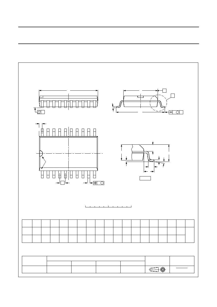
PACKAGE OUTLINE
UNIT
A
max.
A
1
A
2
A
3
b
p
c
D
(1)
E
(1)
(1)
e
H
E
L
L
p
Q
Z
y
w
v
REFERENCES
OUTLINE
VERSION
EUROPEAN
PROJECTION
ISSUE DATE
IEC
JEDEC
EIAJ
mm
inches
2.65
0.30
0.10
2.45
2.25
0.49
0.36
0.32
0.23
13.0
12.6
7.6
7.4
1.27
10.65
10.00
1.1
1.0
0.9
0.4
8
0
o
o
0.25
0.1
DIMENSIONS (inch dimensions are derived from the original mm dimensions)
Note
1. Plastic or metal protrusions of 0.15 mm maximum per side are not included.
1.1
0.4
SOT163-1
10
20
w
M
b
p
detail X
Z
e
11
1
D
y
0.25
075E04
MS-013AC
pin 1 index
0.10
0.012
0.004
0.096
0.089
0.019
0.014
0.013
0.009
0.51
0.49
0.30
0.29
0.050
1.4
0.055
0.419
0.394
0.043
0.039
0.035
0.016
0.01
0.25
0.01
0.004
0.043
0.016
0.01
0
5
10 mm
scale
X
A
A
1
A
2
H
E
L
p
Q
E
c
L
v
M
A
(A )
3
A
SO20: plastic small outline package; 20 leads; body width 7.5 mm
SOT163-1
95-01-24
97-05-22

1998 May 07
12
Philips Semiconductors
Product specification
Multiple voltage regulator with battery
detection
TDA3606A
SOLDERING
Introduction
There is no soldering method that is ideal for all IC
packages. Wave soldering is often preferred when
through-hole and surface mounted components are mixed
on one printed-circuit board. However, wave soldering is
not always suitable for surface mounted ICs, or for
printed-circuits with high population densities. In these
situations reflow soldering is often used.
This text gives a very brief insight to a complex technology.
A more in-depth account of soldering ICs can be found in
our
"Data Handbook IC26; Integrated Circuit Packages"
(order code 9398 652 90011).
Reflow soldering
Reflow soldering techniques are suitable for all SO
packages.
Reflow soldering requires solder paste (a suspension of
fine solder particles, flux and binding agent) to be applied
to the printed-circuit board by screen printing, stencilling or
pressure-syringe dispensing before package placement.
Several techniques exist for reflowing; for example,
thermal conduction by heated belt. Dwell times vary
between 50 and 300 seconds depending on heating
method. Typical reflow temperatures range from
215 to 250
∞
C.
Preheating is necessary to dry the paste and evaporate
the binding agent. Preheating duration: 45 minutes at
45
∞
C.
Wave soldering
Wave soldering techniques can be used for all SO
packages if the following conditions are observed:
∑
A double-wave (a turbulent wave with high upward
pressure followed by a smooth laminar wave) soldering
technique should be used.
∑
The longitudinal axis of the package footprint must be
parallel to the solder flow.
∑
The package footprint must incorporate solder thieves at
the downstream end.
During placement and before soldering, the package must
be fixed with a droplet of adhesive. The adhesive can be
applied by screen printing, pin transfer or syringe
dispensing. The package can be soldered after the
adhesive is cured.
Maximum permissible solder temperature is 260
∞
C, and
maximum duration of package immersion in solder is
10 seconds, if cooled to less than 150
∞
C within
6 seconds. Typical dwell time is 4 seconds at 250
∞
C.
A mildly-activated flux will eliminate the need for removal
of corrosive residues in most applications.
Repairing soldered joints
Fix the component by first soldering two diagonally-
opposite end leads. Use only a low voltage soldering iron
(less than 24 V) applied to the flat part of the lead. Contact
time must be limited to 10 seconds at up to 300
∞
C. When
using a dedicated tool, all other leads can be soldered in
one operation within 2 to 5 seconds between
270 and 320
∞
C.

1998 May 07
13
Philips Semiconductors
Product specification
Multiple voltage regulator with battery
detection
TDA3606A
DEFINITIONS
LIFE SUPPORT APPLICATIONS
These products are not designed for use in life support appliances, devices, or systems where malfunction of these
products can reasonably be expected to result in personal injury. Philips customers using or selling these products for
use in such applications do so at their own risk and agree to fully indemnify Philips for any damages resulting from such
improper use or sale.
Data sheet status
Objective specification
This data sheet contains target or goal specifications for product development.
Preliminary specification
This data sheet contains preliminary data; supplementary data may be published later.
Product specification
This data sheet contains final product specifications.
Limiting values
Limiting values given are in accordance with the Absolute Maximum Rating System (IEC 134). Stress above one or
more of the limiting values may cause permanent damage to the device. These are stress ratings only and operation
of the device at these or at any other conditions above those given in the Characteristics sections of the specification
is not implied. Exposure to limiting values for extended periods may affect device reliability.
Application information
Where application information is given, it is advisory and does not form part of the specification.

1998 May 07
14
Philips Semiconductors
Product specification
Multiple voltage regulator with battery
detection
TDA3606A
NOTES

1998 May 07
15
Philips Semiconductors
Product specification
Multiple voltage regulator with battery
detection
TDA3606A
NOTES

Internet: http://www.semiconductors.philips.com
Philips Semiconductors ≠ a worldwide company
© Philips Electronics N.V. 1998
SCA59
All rights are reserved. Reproduction in whole or in part is prohibited without the prior written consent of the copyright owner.
The information presented in this document does not form part of any quotation or contract, is believed to be accurate and reliable and may be changed
without notice. No liability will be accepted by the publisher for any consequence of its use. Publication thereof does not convey nor imply any license
under patent- or other industrial or intellectual property rights.
Middle East: see Italy
Netherlands: Postbus 90050, 5600 PB EINDHOVEN, Bldg. VB,
Tel. +31 40 27 82785, Fax. +31 40 27 88399
New Zealand: 2 Wagener Place, C.P.O. Box 1041, AUCKLAND,
Tel. +64 9 849 4160, Fax. +64 9 849 7811
Norway: Box 1, Manglerud 0612, OSLO,
Tel. +47 22 74 8000, Fax. +47 22 74 8341
Pakistan: see Singapore
Philippines: Philips Semiconductors Philippines Inc.,
106 Valero St. Salcedo Village, P.O. Box 2108 MCC, MAKATI,
Metro MANILA, Tel. +63 2 816 6380, Fax. +63 2 817 3474
Poland: Ul. Lukiska 10, PL 04-123 WARSZAWA,
Tel. +48 22 612 2831, Fax. +48 22 612 2327
Portugal: see Spain
Romania: see Italy
Russia: Philips Russia, Ul. Usatcheva 35A, 119048 MOSCOW,
Tel. +7 095 755 6918, Fax. +7 095 755 6919
Singapore: Lorong 1, Toa Payoh, SINGAPORE 319762,
Tel. +65 350 2538, Fax. +65 251 6500
Slovakia: see Austria
Slovenia: see Italy
South Africa: S.A. PHILIPS Pty Ltd., 195-215 Main Road Martindale,
2092 JOHANNESBURG, P.O. Box 7430 Johannesburg 2000,
Tel. +27 11 470 5911, Fax. +27 11 470 5494
South America: Al. Vicente Pinzon, 173, 6th floor,
04547-130 S√O PAULO, SP, Brazil,
Tel. +55 11 821 2333, Fax. +55 11 821 2382
Spain: Balmes 22, 08007 BARCELONA,
Tel. +34 3 301 6312, Fax. +34 3 301 4107
Sweden: Kottbygatan 7, Akalla, S-16485 STOCKHOLM,
Tel. +46 8 5985 2000, Fax. +46 8 5985 2745
Switzerland: Allmendstrasse 140, CH-8027 ZÐRICH,
Tel. +41 1 488 2741 Fax. +41 1 488 3263
Taiwan: Philips Semiconductors, 6F, No. 96, Chien Kuo N. Rd., Sec. 1,
TAIPEI, Taiwan Tel. +886 2 2134 2865, Fax. +886 2 2134 2874
Thailand: PHILIPS ELECTRONICS (THAILAND) Ltd.,
209/2 Sanpavuth-Bangna Road Prakanong, BANGKOK 10260,
Tel. +66 2 745 4090, Fax. +66 2 398 0793
Turkey: Talatpasa Cad. No. 5, 80640 GÐLTEPE/ISTANBUL,
Tel. +90 212 279 2770, Fax. +90 212 282 6707
Ukraine: PHILIPS UKRAINE, 4 Patrice Lumumba str., Building B, Floor 7,
252042 KIEV, Tel. +380 44 264 2776, Fax. +380 44 268 0461
United Kingdom: Philips Semiconductors Ltd., 276 Bath Road, Hayes,
MIDDLESEX UB3 5BX, Tel. +44 181 730 5000, Fax. +44 181 754 8421
United States: 811 East Arques Avenue, SUNNYVALE, CA 94088-3409,
Tel. +1 800 234 7381
Uruguay: see South America
Vietnam: see Singapore
Yugoslavia: PHILIPS, Trg N. Pasica 5/v, 11000 BEOGRAD,
Tel. +381 11 625 344, Fax.+381 11 635 777
For all other countries apply to: Philips Semiconductors,
International Marketing & Sales Communications, Building BE-p, P.O. Box 218,
5600 MD EINDHOVEN, The Netherlands, Fax. +31 40 27 24825
Argentina: see South America
Australia: 34 Waterloo Road, NORTH RYDE, NSW 2113,
Tel. +61 2 9805 4455, Fax. +61 2 9805 4466
Austria: Computerstr. 6, A-1101 WIEN, P.O. Box 213, Tel. +43 160 1010,
Fax. +43 160 101 1210
Belarus: Hotel Minsk Business Center, Bld. 3, r. 1211, Volodarski Str. 6,
220050 MINSK, Tel. +375 172 200 733, Fax. +375 172 200 773
Belgium: see The Netherlands
Brazil: see South America
Bulgaria: Philips Bulgaria Ltd., Energoproject, 15th floor,
51 James Bourchier Blvd., 1407 SOFIA,
Tel. +359 2 689 211, Fax. +359 2 689 102
Canada: PHILIPS SEMICONDUCTORS/COMPONENTS,
Tel. +1 800 234 7381
China/Hong Kong: 501 Hong Kong Industrial Technology Centre,
72 Tat Chee Avenue, Kowloon Tong, HONG KONG,
Tel. +852 2319 7888, Fax. +852 2319 7700
Colombia: see South America
Czech Republic: see Austria
Denmark: Prags Boulevard 80, PB 1919, DK-2300 COPENHAGEN S,
Tel. +45 32 88 2636, Fax. +45 31 57 0044
Finland: Sinikalliontie 3, FIN-02630 ESPOO,
Tel. +358 9 615800, Fax. +358 9 61580920
France: 51 Rue Carnot, BP317, 92156 SURESNES Cedex,
Tel. +33 1 40 99 6161, Fax. +33 1 40 99 6427
Germany: Hammerbrookstraþe 69, D-20097 HAMBURG,
Tel. +49 40 23 53 60, Fax. +49 40 23 536 300
Greece: No. 15, 25th March Street, GR 17778 TAVROS/ATHENS,
Tel. +30 1 4894 339/239, Fax. +30 1 4814 240
Hungary: see Austria
India: Philips INDIA Ltd, Band Box Building, 2nd floor,
254-D, Dr. Annie Besant Road, Worli, MUMBAI 400 025,
Tel. +91 22 493 8541, Fax. +91 22 493 0966
Indonesia: PT Philips Development Corporation, Semiconductors Division,
Gedung Philips, Jl. Buncit Raya Kav.99-100, JAKARTA 12510,
Tel. +62 21 794 0040 ext. 2501, Fax. +62 21 794 0080
Ireland: Newstead, Clonskeagh, DUBLIN 14,
Tel. +353 1 7640 000, Fax. +353 1 7640 200
Israel: RAPAC Electronics, 7 Kehilat Saloniki St, PO Box 18053,
TEL AVIV 61180, Tel. +972 3 645 0444, Fax. +972 3 649 1007
Italy: PHILIPS SEMICONDUCTORS, Piazza IV Novembre 3,
20124 MILANO, Tel. +39 2 6752 2531, Fax. +39 2 6752 2557
Japan: Philips Bldg 13-37, Kohnan 2-chome, Minato-ku, TOKYO 108,
Tel. +81 3 3740 5130, Fax. +81 3 3740 5077
Korea: Philips House, 260-199 Itaewon-dong, Yongsan-ku, SEOUL,
Tel. +82 2 709 1412, Fax. +82 2 709 1415
Malaysia: No. 76 Jalan Universiti, 46200 PETALING JAYA, SELANGOR,
Tel. +60 3 750 5214, Fax. +60 3 757 4880
Mexico: 5900 Gateway East, Suite 200, EL PASO, TEXAS 79905,
Tel. +9-5 800 234 7381
Printed in The Netherlands
545102/1200/02/pp16
Date of release: 1998 May 07
Document order number:
9397 750 03768