 | –≠–ª–µ–∫—Ç—Ä–æ–Ω–Ω—ã–π –∫–æ–º–ø–æ–Ω–µ–Ω—Ç: TDA3866 | –°–∫–∞—á–∞—Ç—å:  PDF PDF  ZIP ZIP |

DATA SHEET
Preliminary specification
File under Integrated Circuits, IC02
January 1992
INTEGRATED CIRCUITS
TDA3866
Quasi-split sound processor for all
standards
January 1992
2
Philips Semiconductors
Preliminary specification
Quasi-split sound processor for all standards
TDA3866
FEATURES
∑
Quasi-split sound processor for all standards e. g. B/G
(FM sound) and L (AM sound)
∑
AF2 signal automatically muted (at B/G) by the input
signal level
∑
AM signal processing for L standard and switching over
the audio signal
∑
Stereo-matrix correction
∑
Layout-compatible with TDA3858 (32 pins) and
TDA3857 (20 pins)
∑
AM output level typically 500 mV at m = 0.54 (
+
2.5 dB in
comparison to TDA3856)
GENERAL DESCRIPTION
Separate symmetrical IF inputs for FM or AM sound.
Gain controlled wideband IF amplifier, input select switch.
AGC generation due to peak sync for FM or mean signal
level for AM. Reference amplifier for the regeneration of
the vision carrier. Optimized limiting amplifier for AM
suppression in the regenerated vision carrier signal and
90
∞
phase shifter.
Intercarrier mixer for FM sound, output with low-pass filter.
Separate signal processing for 5.5 and 5.74 MHz
intercarriers.
Wide supply voltage range, only 300 mW power
dissipation at 5 V.
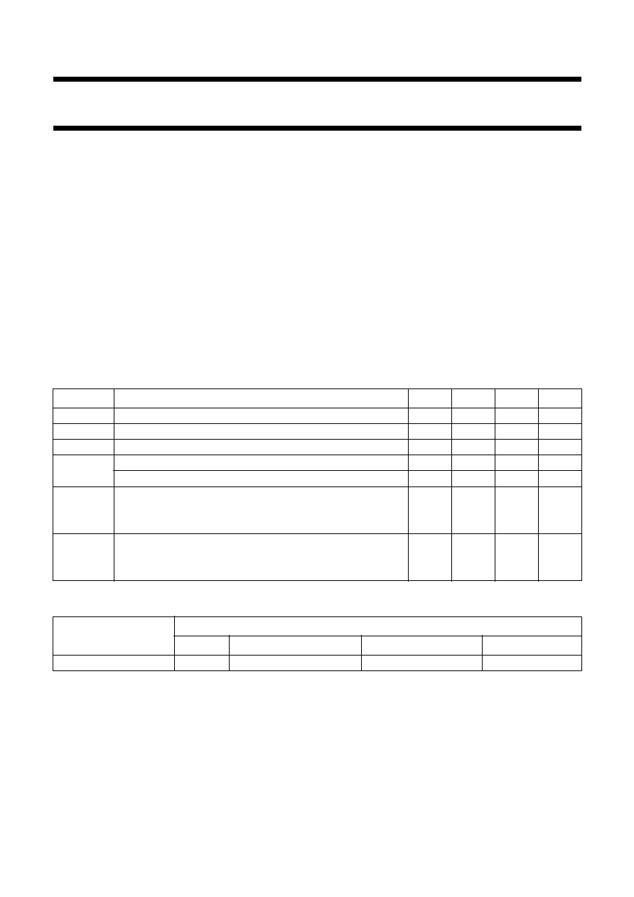
QUICK REFERENCE DATA
ORDERING AND PACKAGE INFORMATION
Note
1. SOT234-1; 1997 January 8.
SYMBOL
PARAMETER
MIN.
TYP.
MAX.
UNIT
V
P
supply voltage (pin 21)
4.5
5
8.8
V
I
P
supply current
-
60
72
mA
V
i IF
IF input sensitivity (
-
3 dB)
-
70
100
µ
V
V
o
audio output signal for FM standard B/G (RMS value)
-
1
-
V
audio output signal for AM standard L (RMS value)
-
0.5
-
V
THD
total harmonic distortion
for FM
-
0.5
-
%
for AM
-
1
-
%
S/N (W)
weighted signal-to-noise ratio
for FM
-
68
-
dB
for AM
-
56
-
dB
EXTENDED TYPE
NUMBER
PACKAGE
PINS
PIN POSITION
MATERIAL
CODE
TDA3866
24
shrink DIL
plastic
SOT234
(1)

January 1992
3
Philips Semiconductors
Preliminary specification
Quasi-split sound processor for all standards
TDA3866
Fig.1 Block diagram (B/G and L).

January 1992
4
Philips Semiconductors
Preliminary specification
Quasi-split sound processor for all standards
TDA3866
PINNING
SYMBOL
PIN
DESCRIPTION
AMIF1
1
AM IF difference input 1 for L standard (32.4 MHz)
AMIF2
2
AM IF difference input 2 for L standard
C
AGC
3
charge capacitor for AGC (FM and AM)
C
AM
4
charge capacitor for AM AGC
MODE
5
3-state input for standard select
FM2R1
6
reference circuit for FM2 (5.74 MHz)
FM2R2
7
reference circuit for FM2 (5,74 MHz)
AF2
8
AF2 output (AF out of 5.74 MHz)
AF1
9
AF1 output (AF out of 5.5 MHz or AM)
FM1R1
10
reference circuit for FM1 (5.5 MHz)
FM1R2
11
reference circuit for FM1 (5.5 MHz)
VC-R1
12
reference circuit for the vision carrier (38.9 MHz)
VC-R2
13
reference circuit for the vision carrier (38.9 MHz)
C
AFAM
14
DC-decoupling capacitor for AM demodulator (AF-AM)
FM1I
15
intercarrier input for FM1 (5.5 MHz)
C
AF1
16
DC-decoupling capacitor for FM1 demodulator (AF1)
ICO
17
intercarrier output signal (5.5/5.74 MHz)
C
AF2
18
DC-decoupling capacitor for FM2 demodulator (AF2)
FM2I
19
intercarrier input for FM2 (5.74 MHz)
GND
20
ground (0 V)
V
P
21
+
5 ...
+
8 V supply voltage
C
ref
22
charge capacitor for reference voltage
FMIF1
23
IF difference input 1 for B/G standard (38.9 MHz)
FMIF2
24
IF difference input 2 for B/G standard (38.9 MHz)
PIN CONFIGURATION
Fig.2 Pin configuration.

January 1992
5
Philips Semiconductors
Preliminary specification
Quasi-split sound processor for all standards
TDA3866
FUNCTIONAL DESCRIPTION
The quasi-split sound processor is for
all standards. Dependent on the
voltage on pin 5 either FM mode
(B/G) or AM mode (L) is selected.
B/G standard (FM mode):
Pins 23 and 24 are active, AGC
detector uses peak sync level. Sound
carrier SC1 (5.5 MHz) provides AF1,
sound carrier SC2 (5.74 MHz)
provides AF2. With no sound carrier
SC2 on pin 19, AF2 output is muted
(in mid-position of the standard select
switch FM mode without muting of
AF2 is selected).
The mute circuit prevents false signal
recognition in the stereo decoder at
high IF signal levels when no second
sound carrier exists (mono) and an
AF signal is present in the
identification signal frequency range.
With 1 mV on pin 19, under
measurement conditions, AF2 is
switched on (see limiting amplifier).
Weak input signals at pins 23 and 24
generate noise on pin 19, which is
present in the intercarrier signal and
passes through the 5.74 MHz filter.
Noise on pin 19 inhibits muting. No
misinterpretation due to white noise
occurs in the stereo decoder; when
non-correlated noise masks the
identification signal frequencies,
which may be present in sustained
tone signals. The stereo decoder
remains switched to mono.
The series capacitor C
s
in 38.9 MHz
resonant circuit provides a notch at
the sound carrier frequency in order
to provide more attenuation for the
sound carrier in the vision carrier
reference channel. The ratio of
parallel/series capacitor depends on
the ratio of VC/SC frequency and has
to be adapted to other TV
transmission standards if necessary,
according to the formula
C
S
= C
P
(f
VC
/f
SC
)
2
-
C
P
.
The result is an improved "intercarrier
buzz" (up to 10 dB improvement in
sound channel 2 with 250 kHz video
modulation for B/G stereo) or
suppression of 350 kHz video
modulated beat frequency in the
digitally-modulated NICAM
subcarrier.
The picture carrier for quadrature
demodulation in the intercarrier mixer
is not exactly 90 degrees due to the
shift variation in the integrated phase
shift network. The tuning of the LC
reference circuit to provide optimal
video suppression at the intercarrier
output is not the same as that to
provide optimal intercarrier buzz
suppression. In order to optimize the
AF signal performance, a fine tuning
for the optimal S/N at the sound
channel 2 (from 5.74 MHz) may be
performed with a 250 kHz square
wave video modulation.
Measurements at the demodulators:
For all signal-to-noise measurements
the generator must meet the following
specifications;
phase modulation errors
<
0.5 degree
for B/W-jumps intercarrier
signal-to-noise ratio as measured
with "TV-demodulator AMF2"
(weighted S/N) must be
>
60 dB at
6 kHz sine wave modulation of the
B/W-signal.
Signal-to-noise ratios are measured
with
f =
±
50 kHz deviation and
f
mod
= 1 kHz; with a deviation
of
±
27 kHz the S/N ratio is
deteriorated by 5.3 dB.
L standard (AM mode): Pins 1 and 2
are active, AGC detector uses mean
signal level. The audio signal from the
AM demodulator is output on AF1,
with AF2 output muted.

January 1992
6
Philips Semiconductors
Preliminary specification
Quasi-split sound processor for all standards
TDA3866
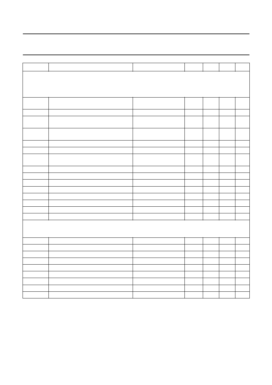
LIMITING VALUES
In accordance with the Absolute Maximum System (IEC 134).
Note
1. Equivalent to discharging a 200 pF capacitor through a 0
series resistor.
SYMBOL
PARAMETER
MIN.
MAX.
UNIT
V
P
supply voltages (pin 21)
-
8.8
V
V
n
input and output voltage (pins 1, 2, 5, 8, 9, 15, 17, 19, 23
and 24)
0
V
P
V
P
tot
total power dissipation
0
635
mW
T
stg
storage temperature range
-
25
150
∞
C
T
amb
operating ambient temperature range
0
70
∞
C
V
ESD
electrostatic handling
(1)
±
500
-
V
all pins except 1, 2, 23 and 24
pins 1, 2, 23 and 24
+
400
-
V
pins 1, 2, 23 and 24
-
500
-
V

January 1992
7
Philips Semiconductors
Preliminary specification
Quasi-split sound processor for all standards
TDA3866
CHARACTERISTICS
V
P
= 5 V and T
amb
= 25
∞
C, measurements taken in Fig.3 with f
VC
= 38.9 MHz, f
SC1
= 33.4 MHz and f
SC2
= 33.158 MHz.
Vision carrier (VC) modulated with different video signals, modulation depth 100 % (proportional to 10 % residual
carrier).
Vision carrier amplitude (RMS value) V
i VC
= 10 mV; vision to sound carrier ratios are VC/SC1 = 13 dB and
VC/SC2 = 20 dB. Sound carriers (SC1, SC2) modulated with f = 1 kHz and deviation
f = 50 kHz unless otherwise
specified.
SYMBOL
PARAMETER
CONDITIONS
MIN.
TYP.
MAX.
UNIT
V
P
supply voltage range (pin 21)
4.5
5
8.8
V
I
P
supply current (pin 21)
48
60
72
mA
IF source control (pin 5)
V
5
input voltage in order to obtain standards
B/G (FM) with automatic muting
pin 5 connected
2.8
-
V
P
V
pin 5 open-circuit
-
2.8
-
V
B/G (FM) without muting
pin 5 connected
1.3
-
2.3
V
22 k
to GND
(alternative measure)
-
1.8
-
V
L (AM sound)
pin 5 connected
0
-
0.8
V
I
5
input current
V
5
= V
P
-
-
100
µ
A
V
5
= 0
-
-
-
300
µ
A
IF input not activated (pins 1-2 or 23-24)
R
I
input resistance
-
-
100
V
DC
DC input voltage (pins 1, 2, 23 and 24)
internally set LOW
-
-
0.1
V
1,2-23,24
crosstalk attenuation of IF input switch
note 1
50
56
-
dB
IF amplifier (pins 1-2 or 23-24)
R
I
input resistance
1.75
2.2
2.65
k
C
I
input capacitance
1.0
1.5
2.2
pF
V
I
DC potential, voltage (pins 1, 2, 23, 24)
-
1.75
-
V
V
i IF
maximum input signal (RMS value)
V
o
=
+
1 dB
70
100
-
mV
input signal sensitivity B/G standard
(RMS value, pins 23-24)
-
3 dB intercarrier signal
reduction on pin 17
-
70
100
µ
V
input signal sensitivity L standard
(RMS value, pins 1-2)
-
3 dB intercarrier signal
reduction on pin 9
-
70
100
µ
V
G
v
IF gain control range
60
63
-
dB
B
IF bandwidth
-
3 dB
50
70
-
MHz
V
3
voltage range for gain control (pin 3)
G
min
-
G
max
1.7
-
2.6
V

January 1992
8
Philips Semiconductors
Preliminary specification
Quasi-split sound processor for all standards
TDA3866
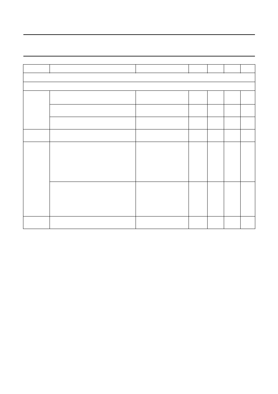
Resonance amplifier (pins 12-13)
V
o
vision carrier amplitude
(peak-to-peak value)
f
o
= 38.9 MHz
-
270
-
mV
R
12-13
operating resistance
-
4
-
k
L
inductance
Fig.3 and 5
-
0.247
-
µ
H
C
capacitance
C
S
= 27 pF
-
68
-
pF
Q
L
Q-factor of resonant circuit
Q
o
= 90
-
40
-
V
12, 13
DC voltage (pins 12 and 13)
-
V
P
-
1
-
V
Intercarrier mixer output (pin 17)
V
o
output signal for 5.5 MHz (RMS value)
71
95
125
mV
output signal for 5.74 MHz (RMS value)
32
43
56
mV
B
IF bandwidth
-
1 dB
-
8.5
-
MHz
-
3 dB
-
10
-
MHz
V
VID
/V
17
residual video AM on intercarrier
note 2
-
3
10
%
V
VC
residual vision carrier (RMS value)
1st/2nd harmonic;
(38.9/77.8 MHz)
-
0.5
1
mV
R
17
output resistance (emitter follower)
1 mA emitter current
-
30
-
I
o
allowable AC output current (pin 17)
-
-
±
0.7
mA
I
17
allowable DC output current
-
-
-
2
mA
V
17
DC voltage
-
1.75
-
V
Limiting amplifiers (pins 15 and 19)
V
i
minimum input signal (RMS value)
-
3 dB AF signal
-
300
450
µ
V
maximum input signal (RMS value)
200
-
-
mV
R
15, 19
input resistance
-
560
-
V
15, 19
DC voltage
-
0
-
V
V
i
level detector threshold for no muting
(RMS value, pin 19)
only 5.74 MHz channel
-
1
-
mV
V
i
hysteresis of level detector
-
5
-
dB
SYMBOL
PARAMETER
CONDITIONS
MIN.
TYP.
MAX.
UNIT
January 1992
9
Philips Semiconductors
Preliminary specification
Quasi-split sound processor for all standards
TDA3866
FM1 and FM2 demodulators
Measurements with FM IF input signals of 5.5 MHz and 5.74 MHz with V
i IF (rms)
= 10 mV (f
mod
= 1 kHz, deviation
f =
±
50 kHz) at pins 15 and 19 without ceramic filters, R
S
= 50
.
De-emphasis 50
µ
s and V
5
= V
P
(B/G standard). Q
L
-factor = 11 for resonant circuits at pins 6-7 and 10-11.
V
IC
intercarrier signals
(RMS values, pins 6-7 and 10-11)
-
100
-
mV
V
DC
DC voltage (pins 6-7 and 10-11)
-
1.8
-
V
V
o
AF output signals
(RMS values, pins 8 and 9)
0.75
0.95
1.20
V
V
o
difference of AF signals
between channels (pins 8 and 9)
-
-
1
dB
R
8, 9
output resistance
-
100
-
V
8, 9
DC voltage
-
2.1
-
V
I
8, 9
allowed AC current of emitter output
(peak value)
note 3
-
-
±
1.5
mA
I
8, 9
maximum allowed DC output current
-
-
-
2
mA
THD
total harmonic distortion
-
0.5
1.0
%
V
o
AF output signal (RMS value)
THD = 1.5 %
1.25
-
-
V
AM
AM suppression
1 kHz, m = 0.3
48
54
-
dB
S/N(W)
weighted signal-to-noise ratio
CCIR 468-3
64
68
-
dB
B
AF bandwidth
-
3 dB
0.02
-
100
kHz
CR
crosstalk attenuation (pins 9-8)
60
70
-
dB
V
16, 18
DC voltage (pins 16 and 18)
-
1.7
-
V
AM mode, input signal at pins 1-2
SC = 32.4 MHz;
f
mod
= 1 kHz, m = 0.54;
V
i AM
= 10 mV rms
V
o
AF output signal on pin 9 (RMS value)
400
500
600
mV
R
9
output resistance (pin 9)
-
100
-
I
o
maximum AC output current (peak value)
note 3
-
-
±
1.5
mA
I
9
maximum DC output current
-
-
-
2
mA
V
9
DC voltage
-
2.1
-
V
THD
total harmonic distortion
Fig.4
-
1
2
%
S/N(W)
weighted signal-to-noise ratio
CCIR 468-3
50
56
-
dB
B
AF bandwidth
-
3 dB
0.02
-
100
kHz
V
14
DC voltage (pin 14)
-
2
-
V
SYMBOL
PARAMETER
CONDITIONS
MIN.
TYP.
MAX.
UNIT
January 1992
10
Philips Semiconductors
Preliminary specification
Quasi-split sound processor for all standards
TDA3866
Notes to the characteristics
1. Crosstalk attenuation of IF input switch, measured at R
12-13
= 470
(instead of LC circuit);
input signal V
i (rms)
= 20 mV (pins 23-24). AGC voltage V
3
set to a value to achieve V
o (rms)
= 20 mV (pins 12-13).
After switching (V
5
= 0 V) measure attenuation.
IF coupling with OFWG3203 and OFWL9350 (Siemens).
2. Spurious intercarrier AM: m = (A-B)/A (wherein A = signal at sync; B = signal with 100% picture modulation.)
3. For larger current: R
L
>
2.2 k
(pin 8 or 9 to GND) in order to increase the bias current of the output emitter follower.
Audio frequency performance for FM operation in B/G standard (V
5
= V
P
) unless otherwise specified.
Measurements on AF outputs (pins 8 and 9)
V
o
signals attenuation of AF signal switches
mute: AF2 on pin 8
V
5
= 0
70
-
-
dB
AM mode: not required signal
AF1 on pin 9 (from FM)
5.5 MHz on pin 18;
V
5
= 0; V
i
= 10 mV
70
-
-
dB
FM mode: not required signal
AF1 on pin 9 (from AM)
signal for L standard
(pins 1-2); V
5
= V
P
70
-
-
dB
dV
8, 9
DC level deviation (pins 8 and 9)
when switching to FM
or AM sound or Mute
-
5
25
mV
S/N(W)
weighted signal-to-noise ratio
on output pin 9
CCIR 468-3
de-emphasis 50
µ
s
black picture
f
i
= 5.5 MHz
59
63
-
dB
2T/20T pulses with white bar
f
i
= 5.5 MHz
57
61
-
dB
6 kHz sine wave, B/W-modulated
f
i
= 5.5 MHz
52
56
-
dB
250 kHz square wave B/W-modulated
f
i
= 5.5 MHz
50
56
-
dB
on output pin 8
black picture
f
i
= 5.742 MHz
57
61
-
dB
2T/20T pulses with white bar
f
i
= 5.742 MHz
55
59
-
dB
6 kHz sine wave, B/W-modulated
f
i
= 5.742 MHz
50
54
-
dB
250 kHz square wave B/W-modulated
f
i
= 5.742 MHz
50
56
-
dB
RR
ripple rejection
all standards; f
R
= 70 Hz
V
R
= 200 mV (p-p)
30
40
-
dB
SYMBOL
PARAMETER
CONDITIONS
MIN.
TYP.
MAX.
UNIT
January 1992
11
Philips Semiconductors
Preliminary specification
Quasi-split sound processor for all standards
TDA3866
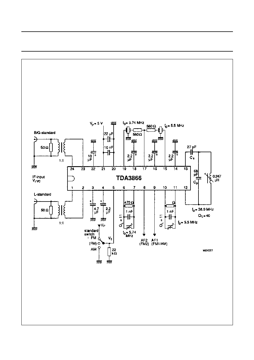
Fig.3 Test and application circuit for standards B/G and L (for application SAW-filters must be used).
January 1992
12
Philips Semiconductors
Preliminary specification
Quasi-split sound processor for all standards
TDA3866
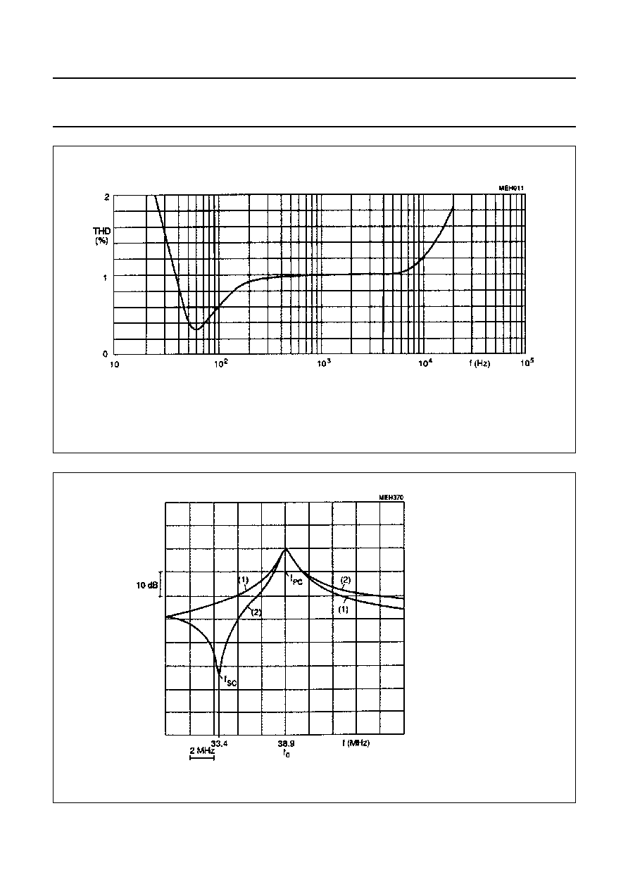
Fig.4 Total harmonic distortion (THD) as a function of audio frequency at AM standard (V
5
= 0).
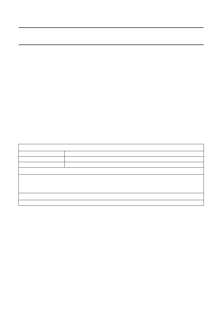
Fig.5 Frequency response of the 38.9 MHz reference circuit.
(1) simple resonance circuit (without C
S
)
(2) resonance circuit with C
S
= 27 pF
C
S
= C
P
(f
VC
/f
SC
)
2
-
C
P
C
S
= 27 pF (Fig.3)

January 1992
13
Philips Semiconductors
Preliminary specification
Quasi-split sound processor for all standards
TDA3866
APPLICATION INFORMATION
Fig.6 Internal circuits; (continued in Fig.7).

January 1992
14
Philips Semiconductors
Preliminary specification
Quasi-split sound processor for all standards
TDA3866
Fig.7 Internal circuits; (continued from Fig.6)

January 1992
15
Philips Semiconductors
Preliminary specification
Quasi-split sound processor for all standards
TDA3866
PACKAGE OUTLINE
UNIT
b
1
c
E
e
M
H
L
REFERENCES
OUTLINE
VERSION
EUROPEAN
PROJECTION
ISSUE DATE
IEC
JEDEC
EIAJ
mm
DIMENSIONS (mm are the original dimensions)
SOT234-1
92-11-17
95-02-04
b
max.
w
M
E
e
1
1.3
0.8
0.53
0.40
0.32
0.23
22.3
21.4
9.1
8.7
3.2
2.8
0.18
1.778
10.16
10.7
10.2
12.2
10.5
1.6
4.7
0.51
3.8
M
H
c
(e )
1
M
E
A
L
seating plane
A
1
w
M
b
1
e
D
A
2
Z
24
1
13
12
b
E
pin 1 index
0
5
10 mm
scale
Note
1. Plastic or metal protrusions of 0.25 mm maximum per side are not included.
(1)
(1)
D
(1)
Z
A
max.
1
2
A
min.
A
max.
SDIP24: plastic shrink dual in-line package; 24 leads (400 mil)
SOT234-1
January 1992
16
Philips Semiconductors
Preliminary specification
Quasi-split sound processor for all standards
TDA3866
SOLDERING
Introduction
There is no soldering method that is ideal for all IC
packages. Wave soldering is often preferred when
through-hole and surface mounted components are mixed
on one printed-circuit board. However, wave soldering is
not always suitable for surface mounted ICs, or for
printed-circuits with high population densities. In these
situations reflow soldering is often used.
This text gives a very brief insight to a complex technology.
A more in-depth account of soldering ICs can be found in
our
"IC Package Databook" (order code 9398 652 90011).
Soldering by dipping or by wave
The maximum permissible temperature of the solder is
260
∞
C; solder at this temperature must not be in contact
with the joint for more than 5 seconds. The total contact
time of successive solder waves must not exceed
5 seconds.
The device may be mounted up to the seating plane, but
the temperature of the plastic body must not exceed the
specified maximum storage temperature (T
stg max
). If the
printed-circuit board has been pre-heated, forced cooling
may be necessary immediately after soldering to keep the
temperature within the permissible limit.
Repairing soldered joints
Apply a low voltage soldering iron (less than 24 V) to the
lead(s) of the package, below the seating plane or not
more than 2 mm above it. If the temperature of the
soldering iron bit is less than 300
∞
C it may remain in
contact for up to 10 seconds. If the bit temperature is
between 300 and 400
∞
C, contact may be up to 5 seconds.
DEFINITIONS
LIFE SUPPORT APPLICATIONS
These products are not designed for use in life support appliances, devices, or systems where malfunction of these
products can reasonably be expected to result in personal injury. Philips customers using or selling these products for
use in such applications do so at their own risk and agree to fully indemnify Philips for any damages resulting from such
improper use or sale.
Data sheet status
Objective specification
This data sheet contains target or goal specifications for product development.
Preliminary specification
This data sheet contains preliminary data; supplementary data may be published later.
Product specification
This data sheet contains final product specifications.
Limiting values
Limiting values given are in accordance with the Absolute Maximum Rating System (IEC 134). Stress above one or
more of the limiting values may cause permanent damage to the device. These are stress ratings only and operation
of the device at these or at any other conditions above those given in the Characteristics sections of the specification
is not implied. Exposure to limiting values for extended periods may affect device reliability.
Application information
Where application information is given, it is advisory and does not form part of the specification.