 | –≠–ª–µ–∫—Ç—Ä–æ–Ω–Ω—ã–π –∫–æ–º–ø–æ–Ω–µ–Ω—Ç: TDA4565 | –°–∫–∞—á–∞—Ç—å:  PDF PDF  ZIP ZIP |

DATA SHEET
Product specification
File under Integrated Circuits, IC02
November 1989
INTEGRATED CIRCUITS
TDA4565
Colour transient improvement
circuit
November 1989
2
Philips Semiconductors
Product specification
Colour transient improvement circuit
TDA4565
GENERAL DESCRIPTION
The TDA4565 is a monolithic integrated circuit for colour transient improvement (CTI) and luminance delay line in gyrator
technique in colour television receivers.
Features
∑
Colour transient improvement for colour difference signals (R-Y) and (B-Y) with transient detecting-, storage- and
switching stages resulting in high transients of colour difference output signals
∑
A luminance signal path (Y) which substitutes the conventional Y-delay coil with an integrated Y-delay line
∑
Switchable delay time from 730 ns to 1000 ns in steps of 90 ns and additional fine adjustment of 50 ns
∑
Two Y output signals; one of 180 ns less delay
QUICK REFERENCE DATA
Note
1. Delay time is proportional to resistor R
14-18
.
R
14-18
also influences the bandwidth; a value of 1.2 k
results in a bandwidth of 5 MHz (typ.).
PACKAGE OUTLINE
18-lead DIL; plastic (SOT102); SOT102-1; 1996 November 27.
PARAMETER
CONDITIONS
SYMBOL
MIN.
TYP.
MAX.
UNIT
Supply voltage (pin 10)
V
P
10.8
12
13.2
V
Supply current (pin 10)
I
P
-
35
50
mA
Y-signal delay at pin 12
S1 open; R
14-18
= 1.2 k
;
(note 1)
V
15-18
= 0 to 2.5 V
t
17-12
670
730
790
ns
V
15-18
= 3.5 to 5.5 V
t
17-12
760
820
880
ns
V
15-18
= 6.5 to 8.5 V
t
17-12
850
910
970
ns
V
15-18
= 9.5 to 12 V
t
17-12
940
1000
1060
ns
Y-signal attenuation
0.5 MHz
Y
0
6.5
8.0
dB
(R-Y) and (B-Y) signal
attenuation
cd
-
1
0
+
1
dB
output transient time
t
tr
-
100
200
ns
November 1989
3
Philips Semiconductors
Product specification
Colour transient improvement circuit
TDA4565
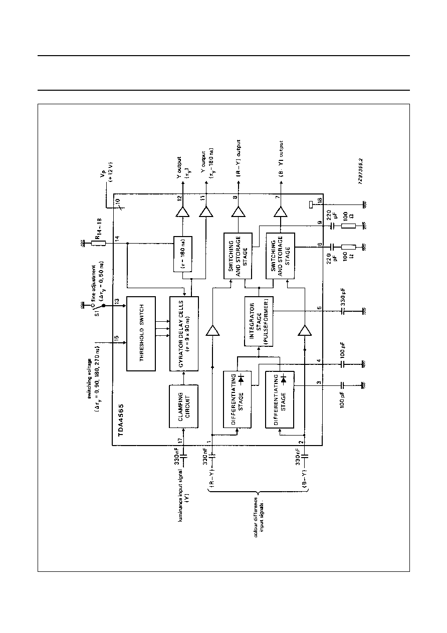
Fig.1 Block diagram.
November 1989
4
Philips Semiconductors
Product specification
Colour transient improvement circuit
TDA4565
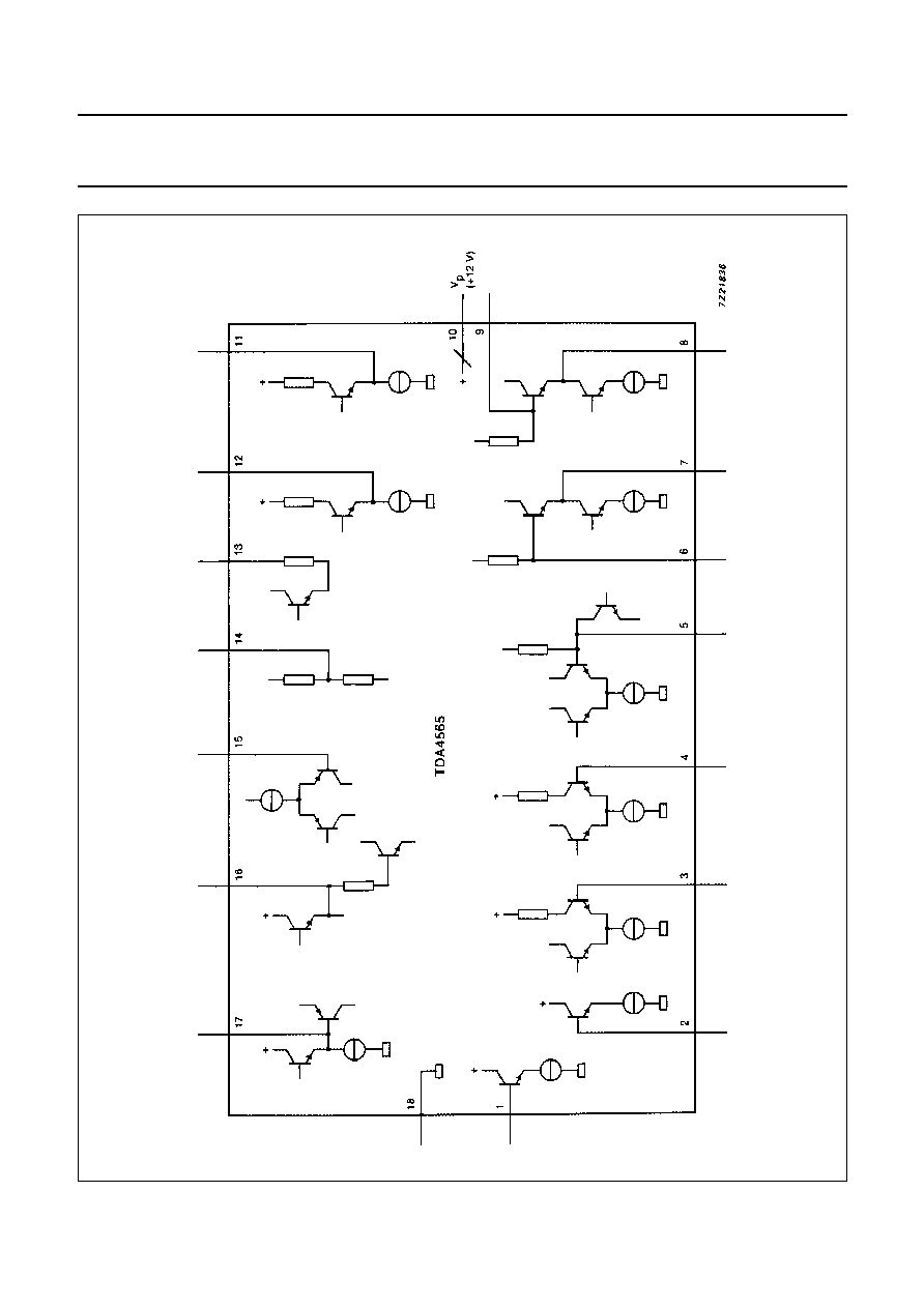
Fig.2 Internal pin circuit diagram.

November 1989
5
Philips Semiconductors
Product specification
Colour transient improvement circuit
TDA4565
RATINGS
Limiting values in accordance with the Absolute Maximum System (IEC 134)
THERMAL RESISTANCE
Note
1. Pins 3, 4, 5, 6, 9, 13 and 14 DC potential not published.
PARAMETER
SYMBOL
MIN.
MAX.
UNIT
Supply voltage range (pin 10)
V
P
= V
10-18
0
13.2
V
Voltage ranges to pin 18 (ground)
at pins 1, 2, 12 and 15
V
n-18
0
V
P
V
at pin 11
V
11-18
0
(V
p
-
3 V)
V
at pin 17
V
17-18
0
7
V
Voltage ranges
at pin 7 to pin 6
V
7-6
0
5
V
at pin 8 to pin 9
V
8-9
0
5
V
Currents
at pins 6, 9
I
6, 9
-
10
+
10
mA
at pins 7, 8, 11 and 12
I
7, 8, 11, 12
internally limited
Total power dissipation
(T
j
= 150
∞
C; T
amb
= 70
∞
C)
P
tot
-
1.1
W
Storage temperature range
T
stg
-
25
+
150
∞
C
Operating ambient temperature range
T
amb
0
+
70
∞
C
From junction to ambient (in free air)
R
th j-a
=
70
K/W

November 1989
6
Philips Semiconductors
Product specification
Colour transient improvement circuit
TDA4565
CHARACTERISTICS
V
P
= V
10-18
= 12 V; T
amb
= 25
∞
C; measured in application circuit Fig.3; unless otherwise specified
PARAMETER
CONDITIONS
SYMBOL
MIN.
TYP.
MAX.
UNIT
Supply (pin 10)
Supply voltage
V
P
10.8
12
13.2
V
Supply current
l
P
-
35
50
mA
Colour difference paths
(R-Y) input voltage
(75% colour bar signal)
(peak-to-peak value)
V
1(p-p)
-
1.05
1.5
V
(B-Y) input voltage
(75% colour bar signal)
(peak-to-peak value)
V
2(p-p)
-
1.33
1.9
V
Input resistance
(R-Y)
R
1-18
8
12
16
k
(B-Y)
R
2-18
8
12
16
k
Internal bias voltage
(R-Y)
V
1-18
3.8
4.3
4.8
V
(B-Y)
V
1-18
3.8
4.3
4.8
V
Signal attenuation
(R-Y)
V
8
/V
1
-
1
0
+
1
dB
(B-Y)
V
7
/V
2
-
1
0
+
1
dB
Output transient time
note 1
t
tr
-
100
200
ns
Output resistance
(B-Y)
R
7-18
-
100
-
(R-Y)
R
8-18
-
100
-
DC output voltage
(B-Y)
V
7-18
3.8
4.3
4.8
V
(R-Y)
V
8
-
18
3.8
4.3
4.8
V
Output current
note 2
source
I
7, 8
0.4
-
-
mA
sink
-
I
7, 8
1.0
-
-
mA
November 1989
7
Philips Semiconductors
Product specification
Colour transient improvement circuit
TDA4565
Y-signal path
Y-input voltage
(composite signal)
capacitive coupling
(peak-to-peak value)
V
17(p-p)
-
1
1.4
V
Internal bias voltage
during clamping
V
17-18
1.3
1.5
1.7
V
Input current
during picture content
I
17
-
8
12
µ
A
during sync. pulse
-
I
17
-
100
150
µ
A
Y-signal delay at pin 12
S1 open;
R
14
= 1.2 k
;
(notes 3 and 4)
at V
15-18
= 0 to 2.5 V
t
17-18
670
730
790
ns
at V
15-18
= 3.5 to 5.5 V
t
17-18
760
820
880
ns
at V
15-18
= 6.5 to 8.5 V
t
17-18
850
910
970
ns
at V
15-18
= 9.5 to 12 V
t
17-18
940
1000
1060
ns
Fine adjustment of Y-signal
delay for all 4 steps
S1 closed
t
17-12
30
50
70
ns
Signal delay between pin 11
and pin 12
S1 open
t
11-12
160
180
200
ns
Dependency of delay time
on temperature
-
0.001
-
K
-
1
on supply voltage
-
-
0.03
-
V
-
1
Input switching current
-
I
15
-
15
25
µ
A
Y-signal attenuation
f = 0.5 MHz
pin 11 from pin 17
V
11
/V
17
5.0
6.5
8.0
dB
pin 12 from pin 17
V
12
/V
17
5.0
6.5
8.0
dB
Frequency response at
3 MHz referred to 0.5 MHz
note 5
pin 11
0
-
3.0
dB
pin 12
0
-
3.0
dB
PARAMETER
CONDITIONS
SYMBOL
MIN.
TYP.
MAX.
UNIT
t
17
12
≠
t
17
12
≠
. T
j
---------------------------
t
17
12
≠
t
17
12
≠
. V
p
-----------------------------
V
11
3 MHz
)
(
V
11
0.5 MHz
)
(
------------------------------------------
V
12
3 MHz
)
(
V
12
0.5 MHz
)
(
------------------------------------------

November 1989
8
Philips Semiconductors
Product specification
Colour transient improvement circuit
TDA4565
Notes to the characteristics
1. Output signal transient time measured with C
6
-
18
= C
9-18
= 220 pF without resistor (see Fig.3).
2. Output current measured with emitter follower with constant current source of 0.6 mA.
3. R
14-18
influences the bandwidth; a value of 1.2 k
results in a bandwidth of 5 MHz (typ.).
4. Delay time is proportional to resistor R
14-18
. Devices with suffix "A" require the value of the resistor to be 1.15 k
;
a 27 k
resistor connected in parallel with R
14-18
= 1.2 k
.
5. Frequency response measured with V
15-18
= 9.5 V and switch S1 open.
Frequency response at
5 MHz referred to 0.5 MHz
note 5
pin 11
-
3.0
-
2.0
dB
pin 12
-
3.0
-
2.0
dB
DC output voltage
pin 11
V
11
-
18
1.8
2.3
2.6
V
pin 12
V
12
-
18
9.8
10.3
10.8
V
Output current
note 2
source
I
11, 12
-
-
0.4
mA
sink
-
I
11, 12
-
-
1.0
mA
PARAMETER
CONDITIONS
SYMBOL
MIN.
TYP.
MAX.
UNIT
V
11
5 MHz
)
(
V
11
0.5 MHz
)
(
------------------------------------------
V
12
5 MHz
(
V
12
0.5 MHz
)
(
------------------------------------------
November 1989
9
Philips Semiconductors
Product specification
Colour transient improvement circuit
TDA4565
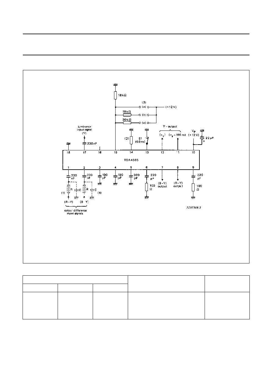
APPLICATION INFORMATION
Table 1
Switching sequence for delay times.
Note
1. When switch (S1) is closed the delay time is increased by 50 ns.
2. Where: X = connection closed; 0 = connection open.
CONNECTION
(2)
VOLTAGE AT PIN 15
DELAY TIME (ns)
(1)
(a)
(b)
(c)
0
0
0
0 to 2.5 V
730
0
0
X
3.5 to 5.5 V
820
0
X
X
6.5 to 8.5 V
910
X
X
X
9.5 to 12 V
1000
Fig.3 Application diagram and test circuit.
(1) Residual carrier reduced to 20 mV peak-to-peak (R = 1 k
, C = 100 pF).
(2) Switching sequence for delay times shown in Table 1.
(3) R
14-18
= 1.2 k
for TDA4565
R
14-18
= 1.15 k
for TDA4565A (27 k
resistor connected in parallel to 1.2 k
).
November 1989
10
Philips Semiconductors
Product specification
Colour transient improvement circuit
TDA4565
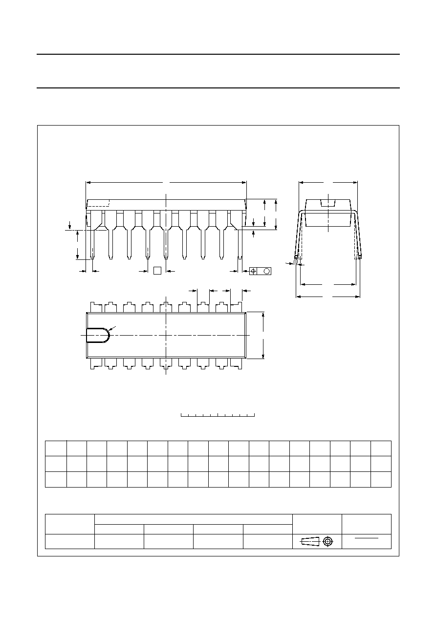
PACKAGE OUTLINE
REFERENCES
OUTLINE
VERSION
EUROPEAN
PROJECTION
ISSUE DATE
IEC
JEDEC
EIAJ
SOT102-1
93-10-14
95-01-23
UNIT
A
max.
1
2
b
1
(1)
(1)
(1)
b
2
c
D
E
e
M
Z
H
L
mm
DIMENSIONS (inch dimensions are derived from the original mm dimensions)
A
min.
A
max.
b
max.
w
M
E
e
1
1.40
1.14
0.53
0.38
0.32
0.23
21.8
21.4
6.48
6.20
3.9
3.4
0.254
2.54
7.62
8.25
7.80
9.5
8.3
0.85
4.7
0.51
3.7
inches
0.055
0.044
0.021
0.015
0.013
0.009
1.40
1.14
0.055
0.044
0.86
0.84
0.26
0.24
0.15
0.13
0.01
0.10
0.30
0.32
0.31
0.37
0.33
0.033
0.19
0.020
0.15
M
H
c
(e )
1
M
E
A
L
seating plane
A
1
w
M
b
1
b
2
e
D
A
2
Z
18
1
10
9
b
E
pin 1 index
0
5
10 mm
scale
Note
1. Plastic or metal protrusions of 0.25 mm maximum per side are not included.
DIP18: plastic dual in-line package; 18 leads (300 mil)
SOT102-1

November 1989
11
Philips Semiconductors
Product specification
Colour transient improvement circuit
TDA4565
SOLDERING
Introduction
There is no soldering method that is ideal for all IC packages. Wave soldering is often preferred when through-hole and
surface mounted components are mixed on one printed-circuit board. However, wave soldering is not always suitable for
surface mounted ICs, or for printed-circuits with high population densities. In these situations reflow soldering is often
used.
This text gives a very brief insight to a complex technology. A more in-depth account of soldering ICs can be found in our
"IC Package Databook" (order code 9398 652 90011).
Soldering by dipping or by wave
The maximum permissible temperature of the solder is 260
∞
C; solder at this temperature must not be in contact with the
joint for more than 5 seconds. The total contact time of successive solder waves must not exceed 5 seconds.
The device may be mounted up to the seating plane, but the temperature of the plastic body must not exceed the
specified maximum storage temperature (T
stg max
). If the printed-circuit board has been pre-heated, forced cooling may
be necessary immediately after soldering to keep the temperature within the permissible limit.
Repairing soldered joints
Apply a low voltage soldering iron (less than 24 V) to the lead(s) of the package, below the seating plane or not more
than 2 mm above it. If the temperature of the soldering iron bit is less than 300
∞
C it may remain in contact for up to
10 seconds. If the bit temperature is between 300 and 400
∞
C, contact may be up to 5 seconds.
DEFINITIONS
LIFE SUPPORT APPLICATIONS
These products are not designed for use in life support appliances, devices, or systems where malfunction of these
products can reasonably be expected to result in personal injury. Philips customers using or selling these products for
use in such applications do so at their own risk and agree to fully indemnify Philips for any damages resulting from such
improper use or sale.
Data sheet status
Objective specification
This data sheet contains target or goal specifications for product development.
Preliminary specification
This data sheet contains preliminary data; supplementary data may be published later.
Product specification
This data sheet contains final product specifications.
Limiting values
Limiting values given are in accordance with the Absolute Maximum Rating System (IEC 134). Stress above one or
more of the limiting values may cause permanent damage to the device. These are stress ratings only and operation
of the device at these or at any other conditions above those given in the Characteristics sections of the specification
is not implied. Exposure to limiting values for extended periods may affect device reliability.
Application information
Where application information is given, it is advisory and does not form part of the specification.