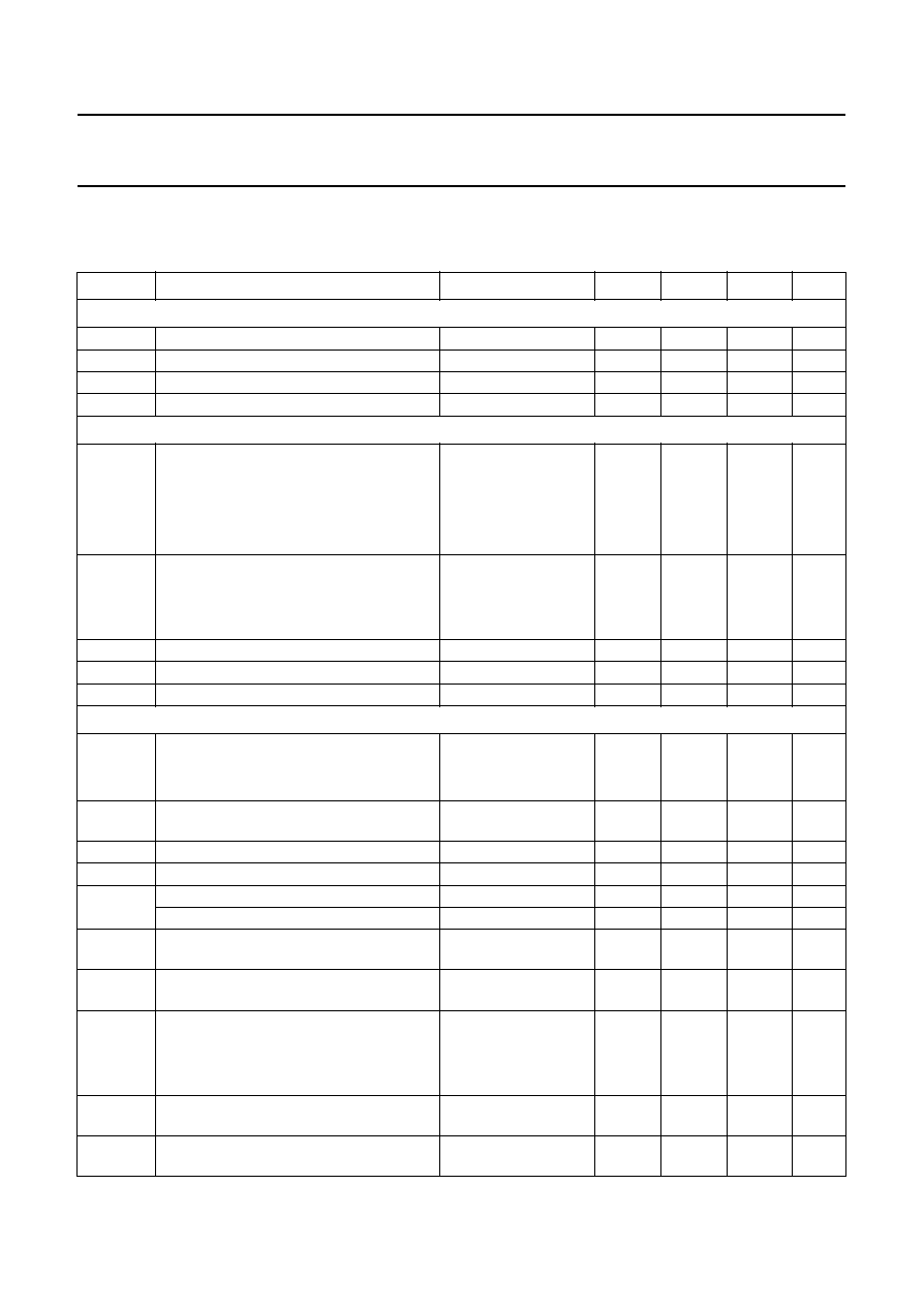
ChipFind - документация

Электронный компонент: TDA4665T/V3

Скачать:  PDF   ZIP

Document Outline

DATA SHEET
Product specification
Supersedes data of 1995 Oct 30
File under Integrated Circuits, IC02
1996 Dec 17
INTEGRATED CIRCUITS
TDA4665
Baseband delay line
1996 Dec 17
2
Philips Semiconductors
Product specification
Baseband delay line
TDA4665
FEATURES
Two comb filters, using the switched-capacitor
technique, for one line delay time (64
s)
Adjustment-free application
No crosstalk between SECAM colour carriers (diaphoty)
Handles negative or positive colour-difference input
signals
Clamping of AC-coupled input signals (
(R
-
Y) and
(B
-
Y))
VCO without external components
3 MHz internal clock signal derived from a 6 MHz CCO,
line-locked by the sandcastle pulse (64
s line)
Sample-and-hold circuits and low-pass filters to
suppress the 3 MHz clock signal
Addition of delayed and non-delayed output signals
Output buffer amplifiers
Comb filtering functions for NTSC colour-difference
signals to suppress cross-colour.
GENERAL DESCRIPTION
The TDA4665 is an integrated baseband delay line circuit
with one line delay. It is suitable for decoders with
colour-difference signal outputs
(R
-
Y) and
(B
-
Y).
QUICK REFERENCE DATA
ORDERING INFORMATION
SYMBOL
PARAMETER
MIN.
TYP.
MAX.
UNIT
V
P1
analog supply voltage (pin 9)
4.5
5
6
V
V
P2
digital supply voltage (pin 1)
4.5
5
6
V
I
P(tot)
total supply current
-
5.5
7.0
mA
V
i(p-p)
(R
-
Y) input signal PAL/NTSC (peak-to-peak value; pin 16)
-
525
-
mV
(B
-
Y) input signal PAL/NTSC (peak-to-peak value; pin 14)
-
665
-
mV
(R
-
Y) input signal SECAM (peak-to-peak value; pin 16)
-
1.05
-
V
(B
-
Y) input signal SECAM (peak-to-peak value; pin 14)
-
1.33
-
V
G
v
gain V
o
/ V
i
of colour-difference output signals
V
11
/ V
16
for PAL and NTSC
5.3
5.8
6.3
dB
V
12
/ V
14
for PAL and NTSC
5.3
5.8
6.3
dB
V
11
/ V
16
for SECAM
-
0.6
-
0.1
+0.4
dB
V
12
/ V
14
for SECAM
-
0.6
-
0.1
+0.4
dB
TYPE
NUMBER
PACKAGE
NAME
DESCRIPTION
VERSION
TDA4665
DIP16
plastic dual in-line package; 16 leads (300 mil)
SOT38-4
TDA4665T
SO16
plastic small outline package; 16 leads; body width 3.9 mm
SOT109-1
1996 Dec 17
3
Philips Semiconductors
Product specification
Baseband delay line
TDA4665
BLOCK DIAGRAM
Fig.1 Block diagram.
handbook, full pagewidth
SANDCASTLE
DETECTOR
FREQUENCY
PHASE
DETECTOR
DIVIDER
BY 192
LP
V
P2
3 MHz shifting clock
1
digital supply
LINE
MEMORY
SIGNAL
CLAMPING
SAMPLE-
AND-HOLD
6 MHz
CCO
DIVIDER
BY 2
LP
addition
stages
output
buffers
colour-difference
output signals
colour-difference
input signals
12
2
5
10
GND1
3
n.c.
6
n.c.
13
n.c.
15
n.c.
7
i.c.
4, 8
(B
-
Y)
(R
-
Y)
(R
-
Y)
(B
-
Y)
V
P1
sandcastle
pulse input
GND2
9
14
LINE
MEMORY
TDA4665
SIGNAL
CLAMPING
pre-amplifiers
SAMPLE-
AND-HOLD
LP
11
16
analog supply
MED848
1996 Dec 17
4
Philips Semiconductors
Product specification
Baseband delay line
TDA4665
PINNING
SYMBOL
PIN
DESCRIPTION
V
P2
1
+5 V supply voltage for digital part
n.c.
2
not connected
GND2
3
ground for digital part (0 V)
i.c.
4
internally connected
SAND
5
sandcastle pulse input
n.c.
6
not connected
i.c.
7
internally connected
i.c.
8
internally connected
V
P1
9
+5 V supply voltage for analog part
GND1
10
ground for analog part (0 V)
V
o(R
-
Y)
11
(R
-
Y) output signal
V
o(B
-
Y)
12
(B
-
Y) output signal
n.c.
13
not connected
V
i(B
-
Y)
14
(B
-
Y) input signal
n.c.
15
not connected
V
i(R
-
Y)
16
(R
-
Y) input signal
handbook, halfpage
TDA4665
MED849
1
2
3
4
5
6
7
8
16
15
14
13
12
11
10
9
VP2
n.c.
GND2
i.c.
SAND
n.c.
i.c.
i.c.
VP1
GND1
Vo(R
-
Y)
Vo(B
-
Y)
n.c.
Vi(B
-
Y)
n.c.
Vi(R
-
Y)
Fig.2 Pin configuration.
LIMITING VALUES
In accordance with the Absolute Maximum Rating System (IEC 134). Ground pins 3 and 10 connected together.
Note
1. Equivalent to discharging a 200 pF capacitor through a 0
series resistor.
THERMAL CHARACTERISTICS
SYMBOL
PARAMETER
MIN.
MAX.
UNIT
V
P1
analog supply voltage (pin 9)
-
0.5
+7
V
V
P2
digital supply voltage (pin 1)
-
0.5
+7
V
V
5
voltage on pin 5
-
0.5
V
P
+ 1.0
V
V
n
voltage on pins 11, 12, 14 and 16
-
0.5
V
P
V
T
stg
storage temperature
-
25
+150
C
T
amb
operating ambient temperature
0
70
C
V
ESD
electrostatic handling for all pins; note 1
-
500
V
SYMBOL
PARAMETER
VALUE
UNIT
R
th j-a
thermal resistance from junction to ambient in free air
SOT38-4
75
K/W
SOT109-1
220
K/W
1996 Dec 17
5
Philips Semiconductors
Product specification
Baseband delay line
TDA4665
CHARACTERISTICS
V
P
= 5.0 V; input signals as specified in characteristics with 75% colour bars;
super-sandcastle frequency of 15.625 kHz; T
amb
= 25
C; measurements taken in Fig.3; unless otherwise specified.
SYMBOL
PARAMETER
CONDITIONS
MIN.
TYP.
MAX.
UNIT
Supply
V
P1
analog supply voltage (pin 9)
4.5
5
6
V
V
P2
digital supply voltage (pin 1)
4.5
5
6
V
I
P1
analog supply current
-
4.8
6.0
mA
I
P2
digital supply current
-
0.7
1.0
mA
Colour-difference input signals
V
i(p-p)
input signal (peak-to-peak value)
note 1
(R
-
Y) PAL and NTSC (pin 16)
-
525
-
mV
(B
-
Y) PAL and NTSC (pin 14)
-
665
-
mV
(R
-
Y) SECAM (pin 16)
-
1.05
-
V
(B
-
Y) SECAM (pin 14)
-
1.33
-
V
V
i(max)(p-p)
maximum symmetrical input signal
(peak-to-peak value)
(R
-
Y) or
(B
-
Y) for PAL and NTSC
before clipping
1
-
-
V
(R
-
Y) or
(B
-
Y) for SECAM
before clipping
2
-
-
V
R
14, 16
input resistance during clamping
-
-
40
k
C
14, 16
input capacitance
-
-
10
pF
V
14, 16
input clamping voltage
proportional to V
P
1.3
1.5
1.7
V
Colour-difference output signals
V
o(p-p)
output signal (peak-to-peak value)
(R
-
Y) on pin 11
all standards
-
1.05
-
V
(B
-
Y) on pin 12
all standards
-
1.33
-
V
V
11
/V
12
ratio of output amplitudes at equal input
signals
V
i(14,16)(p-p)
= 1.33 V
-
0.4
0
+0.4
dB
V
11, 12
DC output voltage
proportional to V
P
2.5
2.9
3.3
V
R
11, 12
output resistance
-
330
400
G
v
gain for PAL and NTSC
ratio V
o
/V
i
5.3
5.8
6.3
dB
gain for SECAM
ratio V
o
/V
i
-
0.6
-
0.1
+0.4
dB
V
n
/V
n+1
ratio of delayed to non-delayed output
signals (pins 11 and 12)
V
i(14,16)(p-p)
= 1.33 V;
SECAM signals
-
0.1
0
+0.1
dB
V
n(rms)
noise voltage (RMS value;
pins 11 and 12)
V
i(14,16)
= 0 V; note 2
-
-
1.2
mV
V
(11,12)(p-p)
unwanted signals (line-locked)
(peak-to-peak value)
V
i(14,16)
= 0 V; active
video; R
S
= 300
meander
-
-
5
mV
spikes
-
-
10
mV
S/N(W)
weighted signal-to-noise ratio
(pins 11 and 12)
V
o(p-p)
= 1 V; note 2
-
54
-
dB
t
d
time difference between non-delayed and
delayed output signals (pins 11 and 12)
63.94
64
64.06
s
1996 Dec 17
6
Philips Semiconductors
Product specification
Baseband delay line
TDA4665
Notes
1. For SECAM the signal must be blanked line-sequentially. The blanking level must be equal to the non-colour signal.
For SECAM, PAL and NTSC the input signal must be equal to the non-colour signal during the internal clamping of
TDA4665 (3 to 1
s before the leading edge of the top pulse of V
5
).
2. Noise voltage at f = 10 kHz to 1 MHz; R
S
< 300
.
3. The leading edge of the burst-key pulse or top pulse is used for timing.
t
d
delay of non-delayed signals
40
60
80
ns
t
tr
transient time of delayed signal on pins 11
respectively 12
300 ns transient of
SECAM signal
-
350
-
ns
transient time of non-delayed signal on
pins 11 respectively 12
300 ns transient of
SECAM signal
-
320
-
ns
Sandcastle pulse input (pin 5)
f
BK
burst-key frequency/sandcastle frequency
14.2
15.625
17.0
kHz
V
5
top pulse voltage
note 3
4.0
-
V
P
+ 1.0 V
V
slice
internal slicing level
V
5
-
1.0
-
V
5
-
0.5 V
I
5
input current
-
-
10
A
C
5
input capacitance
-
-
10
pF
SYMBOL
PARAMETER
CONDITIONS
MIN.
TYP.
MAX.
UNIT
1996 Dec 17
7
Philips Semiconductors
Product specification
Baseband delay line
TDA4665
APPLICATION INFORMATION
Fig.3 Application circuit with TDA4650.
full pagewidth
MED850
10 k
10 k
3.3
k
6.8 k
18 k
10
k
3.3 k
22
F
0.33
F
0.33
F
0.1
F
10
H
100
nF
100
nF
10 nF
47 nF
120 pF
10
nF
10
nF
10
nF
220
pF
220
pF
22
nF
22
nF
220
pF
30
pF
27
pF
27
pF
10
10
560
680
470
330
330
HUE
control
PLL
off
HUE
off
X1
8.8
MHz
30
pF
X2
7.2
MHz
V
P
PAL/NTSC
SECAM
NTSC
FILTERS
PAL
SECAM
Y
CVBS
S-VHS
(Y, C)
NTSC-3.58
NTSC-4.43
chrominance signal
20 to 400 mV (p-p)
16
coil:
Toko 119LN-A3753 GO
14
15
28
24
3
1
27
26
25
12
13
11
10
9
8
7
5
6
4
2
23
22
17
21
19
20
18
LINE-LOCKED PLL /
PULSE PROCESSING
VCO
LINE DELAY
LINE DELAY
(R
-
Y) comb filtering
(B
-
Y) comb filtering
5.1 V
+
12 V
16
14
5
10
9
1
3
11
12
V
o
-
(R
-
Y)
V
o
-
(B
-
Y)
4
8
7
2
6
13
15
i.c.
n.c.
n.c.
n.c.
n.c.
+
5.1 V
+
5.1 V
TDA4650
TDA4665
(1)
(1)
colour-
difference
signals
SSC
(12V)
V
P
=
+
12 V
colour standard
switching signals
1 nF
1 nF
V
i
-
(R
-
Y)
V
i
-
(B
-
Y)
(1)
Capacitors positioned close to pins
9 and 10,
1 and
3.
1996 Dec 17
8
Philips Semiconductors
Product specification
Baseband delay line
TDA4665
PACKAGE OUTLINES
REFERENCES
OUTLINE
VERSION
EUROPEAN
PROJECTION
ISSUE DATE
IEC
JEDEC
EIAJ
SOT38-4
92-11-17
95-01-14
M
H
c
(e )
1
M
E
A
L
seating plane
A
1
w
M
b
1
b
2
e
D
A
2
Z
16
1
9
8
E
pin 1 index
b
0
5
10 mm
scale
Note
1. Plastic or metal protrusions of 0.25 mm maximum per side are not included.
UNIT
A
max.
1
2
b
1
(1)
(1)
(1)
b
2
c
D
E
e
M
Z
H
L
mm
DIMENSIONS (inch dimensions are derived from the original mm dimensions)
A
min.
A
max.
b
max.
w
M
E
e
1
1.73
1.30
0.53
0.38
0.36
0.23
19.50
18.55
6.48
6.20
3.60
3.05
0.254
2.54
7.62
8.25
7.80
10.0
8.3
0.76
4.2
0.51
3.2
inches
0.068
0.051
0.021
0.015
0.014
0.009
1.25
0.85
0.049
0.033
0.77
0.73
0.26
0.24
0.14
0.12
0.01
0.10
0.30
0.32
0.31
0.39
0.33
0.030
0.17
0.020
0.13
DIP16: plastic dual in-line package; 16 leads (300 mil)
SOT38-4
1996 Dec 17
9
Philips Semiconductors
Product specification
Baseband delay line
TDA4665
X
w
M
A
A
1
A
2
b
p
D
H
E
L
p
Q
detail X
E
Z
e
c
L
v
M
A
(A )
3
A
8
9
1
16
y
pin 1 index
UNIT
A
max.
A
1
A
2
A
3
b
p
c
D
(1)
E
(1)
(1)
e
H
E
L
L
p
Q
Z
y
w
v
REFERENCES
OUTLINE
VERSION
EUROPEAN
PROJECTION
ISSUE DATE
IEC
JEDEC
EIAJ
mm
inches
1.75
0.25
0.10
1.45
1.25
0.25
0.49
0.36
0.25
0.19
10.0
9.8
4.0
3.8
1.27
6.2
5.8
0.7
0.6
0.7
0.3
8
0
o
o
0.25
0.1
DIMENSIONS (inch dimensions are derived from the original mm dimensions)
Note
1. Plastic or metal protrusions of 0.15 mm maximum per side are not included.
1.0
0.4
SOT109-1
91-08-13
95-01-23
076E07S
MS-012AC
0.069
0.0098
0.0039
0.057
0.049
0.01
0.019
0.014
0.0098
0.0075
0.39
0.38
0.16
0.15
0.050
1.05
0.041
0.24
0.23
0.028
0.020
0.028
0.012
0.01
0.25
0.01
0.004
0.039
0.016
0
2.5
5 mm
scale
SO16: plastic small outline package; 16 leads; body width 3.9 mm
SOT109-1
1996 Dec 17
10
Philips Semiconductors
Product specification
Baseband delay line
TDA4665
SOLDERING
Introduction
There is no soldering method that is ideal for all IC
packages. Wave soldering is often preferred when
through-hole and surface mounted components are mixed
on one printed-circuit board. However, wave soldering is
not always suitable for surface mounted ICs, or for
printed-circuits with high population densities. In these
situations reflow soldering is often used.
This text gives a very brief insight to a complex technology.
A more in-depth account of soldering ICs can be found in
our
"IC Package Databook" (order code 9398 652 90011).
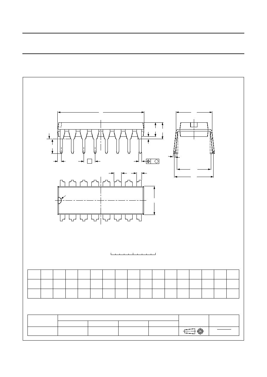
DIP
S
OLDERING BY DIPPING OR BY WAVE
The maximum permissible temperature of the solder is
260
C; solder at this temperature must not be in contact
with the joint for more than 5 seconds. The total contact
time of successive solder waves must not exceed
5 seconds.
The device may be mounted up to the seating plane, but
the temperature of the plastic body must not exceed the
specified maximum storage temperature (T
stg max
). If the
printed-circuit board has been pre-heated, forced cooling
may be necessary immediately after soldering to keep the
temperature within the permissible limit.
R
EPAIRING SOLDERED JOINTS
Apply a low voltage soldering iron (less than 24 V) to the
lead(s) of the package, below the seating plane or not
more than 2 mm above it. If the temperature of the
soldering iron bit is less than 300
C it may remain in
contact for up to 10 seconds. If the bit temperature is
between 300 and 400
C, contact may be up to 5 seconds.
SO
R
EFLOW SOLDERING
Reflow soldering techniques are suitable for all SO
packages.
Reflow soldering requires solder paste (a suspension of
fine solder particles, flux and binding agent) to be applied
to the printed-circuit board by screen printing, stencilling or
pressure-syringe dispensing before package placement.
Several techniques exist for reflowing; for example,
thermal conduction by heated belt. Dwell times vary
between 50 and 300 seconds depending on heating
method. Typical reflow temperatures range from
215 to 250
C.
Preheating is necessary to dry the paste and evaporate
the binding agent. Preheating duration: 45 minutes at
45
C.
W
AVE SOLDERING
Wave soldering techniques can be used for all SO
packages if the following conditions are observed:
A double-wave (a turbulent wave with high upward
pressure followed by a smooth laminar wave) soldering
technique should be used.
The longitudinal axis of the package footprint must be
parallel to the solder flow.
The package footprint must incorporate solder thieves at
the downstream end.
During placement and before soldering, the package must
be fixed with a droplet of adhesive. The adhesive can be
applied by screen printing, pin transfer or syringe
dispensing. The package can be soldered after the
adhesive is cured.
Maximum permissible solder temperature is 260
C, and
maximum duration of package immersion in solder is
10 seconds, if cooled to less than 150
C within
6 seconds. Typical dwell time is 4 seconds at 250
C.
A mildly-activated flux will eliminate the need for removal
of corrosive residues in most applications.
R
EPAIRING SOLDERED JOINTS
Fix the component by first soldering two diagonally-
opposite end leads. Use only a low voltage soldering iron
(less than 24 V) applied to the flat part of the lead. Contact
time must be limited to 10 seconds at up to 300
C. When
using a dedicated tool, all other leads can be soldered in
one operation within 2 to 5 seconds between
270 and 320
C.
1996 Dec 17
11
Philips Semiconductors
Product specification
Baseband delay line
TDA4665
DEFINITIONS
LIFE SUPPORT APPLICATIONS
These products are not designed for use in life support appliances, devices, or systems where malfunction of these
products can reasonably be expected to result in personal injury. Philips customers using or selling these products for
use in such applications do so at their own risk and agree to fully indemnify Philips for any damages resulting from such
improper use or sale.
Data sheet status
Objective specification
This data sheet contains target or goal specifications for product development.
Preliminary specification
This data sheet contains preliminary data; supplementary data may be published later.
Product specification
This data sheet contains final product specifications.
Limiting values
Limiting values given are in accordance with the Absolute Maximum Rating System (IEC 134). Stress above one or
more of the limiting values may cause permanent damage to the device. These are stress ratings only and operation
of the device at these or at any other conditions above those given in the Characteristics sections of the specification
is not implied. Exposure to limiting values for extended periods may affect device reliability.
Application information
Where application information is given, it is advisory and does not form part of the specification.
Internet: http://www.semiconductors.philips.com
Philips Semiconductors a worldwide company
Philips Electronics N.V. 1996
SCA52
All rights are reserved. Reproduction in whole or in part is prohibited without the prior written consent of the copyright owner.
The information presented in this document does not form part of any quotation or contract, is believed to be accurate and reliable and may be changed
without notice. No liability will be accepted by the publisher for any consequence of its use. Publication thereof does not convey nor imply any license
under patent- or other industrial or intellectual property rights.
Netherlands: Postbus 90050, 5600 PB EINDHOVEN, Bldg. VB,
Tel. +31 40 27 82785, Fax. +31 40 27 88399
New Zealand: 2 Wagener Place, C.P.O. Box 1041, AUCKLAND,
Tel. +64 9 849 4160, Fax. +64 9 849 7811
Norway: Box 1, Manglerud 0612, OSLO,
Tel. +47 22 74 8000, Fax. +47 22 74 8341
Philippines: Philips Semiconductors Philippines Inc.,
106 Valero St. Salcedo Village, P.O. Box 2108 MCC, MAKATI,
Metro MANILA, Tel. +63 2 816 6380, Fax. +63 2 817 3474
Poland: Ul. Lukiska 10, PL 04-123 WARSZAWA,
Tel. +48 22 612 2831, Fax. +48 22 612 2327
Portugal: see Spain
Romania: see Italy
Russia: Philips Russia, Ul. Usatcheva 35A, 119048 MOSCOW,
Tel. +7 095 247 9145, Fax. +7 095 247 9144
Singapore: Lorong 1, Toa Payoh, SINGAPORE 1231,
Tel. +65 350 2538, Fax. +65 251 6500
Slovakia: see Austria
Slovenia: see Italy
South Africa: S.A. PHILIPS Pty Ltd., 195-215 Main Road Martindale,
2092 JOHANNESBURG, P.O. Box 7430 Johannesburg 2000,
Tel. +27 11 470 5911, Fax. +27 11 470 5494
South America: Rua do Rocio 220, 5th floor, Suite 51,
04552-903 So Paulo, SO PAULO - SP, Brazil,
Tel. +55 11 821 2333, Fax. +55 11 829 1849
Spain: Balmes 22, 08007 BARCELONA,
Tel. +34 3 301 6312, Fax. +34 3 301 4107
Sweden: Kottbygatan 7, Akalla, S-16485 STOCKHOLM,
Tel. +46 8 632 2000, Fax. +46 8 632 2745
Switzerland: Allmendstrasse 140, CH-8027 ZRICH,
Tel. +41 1 488 2686, Fax. +41 1 481 7730
Taiwan: PHILIPS TAIWAN Ltd., 23-30F, 66,
Chung Hsiao West Road, Sec. 1, P.O. Box 22978,
TAIPEI 100, Tel. +886 2 382 4443, Fax. +886 2 382 4444
Thailand: PHILIPS ELECTRONICS (THAILAND) Ltd.,
209/2 Sanpavuth-Bangna Road Prakanong, BANGKOK 10260,
Tel. +66 2 745 4090, Fax. +66 2 398 0793
Turkey: Talatpasa Cad. No. 5, 80640 GLTEPE/ISTANBUL,
Tel. +90 212 279 2770, Fax. +90 212 282 6707
Ukraine: PHILIPS UKRAINE, 4 Patrice Lumumba str., Building B, Floor 7,
252042 KIEV, Tel. +380 44 264 2776, Fax. +380 44 268 0461
United Kingdom: Philips Semiconductors Ltd., 276 Bath Road, Hayes,
MIDDLESEX UB3 5BX, Tel. +44 181 730 5000, Fax. +44 181 754 8421
United States: 811 East Arques Avenue, SUNNYVALE, CA 94088-3409,
Tel. +1 800 234 7381
Uruguay: see South America
Vietnam: see Singapore
Yugoslavia: PHILIPS, Trg N. Pasica 5/v, 11000 BEOGRAD,
Tel. +381 11 625 344, Fax.+381 11 635 777
For all other countries apply to: Philips Semiconductors, Marketing & Sales Communications,
Building BE-p, P.O. Box 218, 5600 MD EINDHOVEN, The Netherlands, Fax. +31 40 27 24825
Argentina: see South America
Australia: 34 Waterloo Road, NORTH RYDE, NSW 2113,
Tel. +61 2 9805 4455, Fax. +61 2 9805 4466
Austria: Computerstr. 6, A-1101 WIEN, P.O. Box 213,
Tel. +43 1 60 101, Fax. +43 1 60 101 1210
Belarus: Hotel Minsk Business Center, Bld. 3, r. 1211, Volodarski Str. 6,
220050 MINSK, Tel. +375 172 200 733, Fax. +375 172 200 773
Belgium: see The Netherlands
Brazil: see South America
Bulgaria: Philips Bulgaria Ltd., Energoproject, 15th floor,
51 James Bourchier Blvd., 1407 SOFIA,
Tel. +359 2 689 211, Fax. +359 2 689 102
Canada: PHILIPS SEMICONDUCTORS/COMPONENTS,
Tel. +1 800 234 7381
China/Hong Kong: 501 Hong Kong Industrial Technology Centre,
72 Tat Chee Avenue, Kowloon Tong, HONG KONG,
Tel. +852 2319 7888, Fax. +852 2319 7700
Colombia: see South America
Czech Republic: see Austria
Denmark: Prags Boulevard 80, PB 1919, DK-2300 COPENHAGEN S,
Tel. +45 32 88 2636, Fax. +45 31 57 1949
Finland: Sinikalliontie 3, FIN-02630 ESPOO,
Tel. +358 9 615800, Fax. +358 9 61580/xxx
France: 4 Rue du Port-aux-Vins, BP317, 92156 SURESNES Cedex,
Tel. +33 1 40 99 6161, Fax. +33 1 40 99 6427
Germany: Hammerbrookstrae 69, D-20097 HAMBURG,
Tel. +49 40 23 53 60, Fax. +49 40 23 536 300
Greece: No. 15, 25th March Street, GR 17778 TAVROS/ATHENS,
Tel. +30 1 4894 339/239, Fax. +30 1 4814 240
Hungary: see Austria
India: Philips INDIA Ltd, Shivsagar Estate, A Block, Dr. Annie Besant Rd.
Worli, MUMBAI 400 018, Tel. +91 22 4938 541, Fax. +91 22 4938 722
Indonesia: see Singapore
Ireland: Newstead, Clonskeagh, DUBLIN 14,
Tel. +353 1 7640 000, Fax. +353 1 7640 200
Israel: RAPAC Electronics, 7 Kehilat Saloniki St, TEL AVIV 61180,
Tel. +972 3 645 0444, Fax. +972 3 649 1007
Italy: PHILIPS SEMICONDUCTORS, Piazza IV Novembre 3,
20124 MILANO, Tel. +39 2 6752 2531, Fax. +39 2 6752 2557
Japan: Philips Bldg 13-37, Kohnan 2-chome, Minato-ku, TOKYO 108,
Tel. +81 3 3740 5130, Fax. +81 3 3740 5077
Korea: Philips House, 260-199 Itaewon-dong, Yongsan-ku, SEOUL,
Tel. +82 2 709 1412, Fax. +82 2 709 1415
Malaysia: No. 76 Jalan Universiti, 46200 PETALING JAYA, SELANGOR,
Tel. +60 3 750 5214, Fax. +60 3 757 4880
Mexico: 5900 Gateway East, Suite 200, EL PASO, TEXAS 79905,
Tel. +9-5 800 234 7381
Middle East: see Italy
Printed in The Netherlands
537021/1200/03/pp12
Date of release: 1996 Dec 17
Document order number:
9397 750 01376