 | –≠–ª–µ–∫—Ç—Ä–æ–Ω–Ω—ã–π –∫–æ–º–ø–æ–Ω–µ–Ω—Ç: TDA4864J | –°–∫–∞—á–∞—Ç—å:  PDF PDF  ZIP ZIP |

DATA SHEET
Product specification
2003 Oct 31
INTEGRATED CIRCUITS
TDA4864J; TDA4864AJ
Vertical deflection booster

2003 Oct 31
2
Philips Semiconductors
Product specification
Vertical deflection booster
TDA4864J; TDA4864AJ
FEATURES
∑
Power amplifier with differential inputs
∑
Output current up to 2.5 A (p-p)
∑
High vertical deflection frequency up to 200 Hz
∑
High linear sawtooth signal amplification
∑
Flyback generator:
≠ TDA4864J: separate adjustable flyback supply
voltage up to 60 V
≠ TDA4864AJ: internally doubled supply voltage
(two supply voltages only for DC-coupled outputs).
GENERAL DESCRIPTION
The TDA4864J and TDA4864AJ are deflection boosters
for use in vertical deflection systems for frame frequencies
up to 200 Hz.
The TDA4864J needs a separate flyback supply voltage,
so the supply voltages are independently adjustable to
optimize power consumption and flyback time.
For the TDA4864AJ the flyback supply voltage will be
generated internally by doubling the supply voltage and
therefore a separate flyback supply voltage is not needed.
Both circuits provide differential input stages.
QUICK REFERENCE DATA
Measurements referenced to pin GND.
ORDERING INFORMATION
SYMBOL
PARAMETER
CONDITIONS
MIN.
TYP.
MAX.
UNIT
V
P1
supply voltage 1
9
-
30
V
V
P2
supply voltage 2 for vertical output
V
P1
-
1
-
60
V
V
FB
flyback supply voltage of TDA4864J
V
P1
-
1
-
60
V
V
P3
flyback generator output voltage of
TDA4864AJ
I
V-OUT
=
-
1.25 A
0
-
V
P1
+ 2.2 V
V
i
input voltage on
pin INN
1.6
-
V
P1
-
0.5 V
pin INP
1.6
-
V
P1
-
0.5 V
I
P1
supply current 1
during scan
-
6
10
mA
I
P2
quiescent supply current 2
I
V-OUT
= 0
-
25
60
mA
I
V-OUT(p-p)
vertical deflection output current
(peak-to-peak value)
-
-
2.5
A
T
amb
ambient temperature
-
20
-
+75
∞
C
TYPE NUMBER
PACKAGE
NAME
DESCRIPTION
VERSION
TDA4864J
DBS7P
plastic DIL-bent-SIL power package; 7 leads
(lead length 12/11 mm); exposed die pad
SOT524-1
TDA4864AJ
2003 Oct 31
3
Philips Semiconductors
Product specification
Vertical deflection booster
TDA4864J; TDA4864AJ
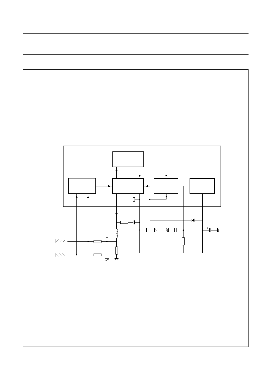
BLOCK DIAGRAM
handbook, full pagewidth
TDA4864J
C1
C4
C2
DIFFERENTIAL
INPUT
STAGE
VERTICAL
OUTPUT
7
6
5
4
3
2
1
REFERENCE
CIRCUIT
FLYBACK
GENERATOR
VP1
VN
GND
deflection
coil
R4
from
deflection controller
THERMAL
PROTECTION
VFB
V-OUT
R1
VF
VP2
RS1
VP
CS1
RP
R3
R2
D1
INN
INP
Fig.1 Block diagram of TDA4864J.
2003 Oct 31
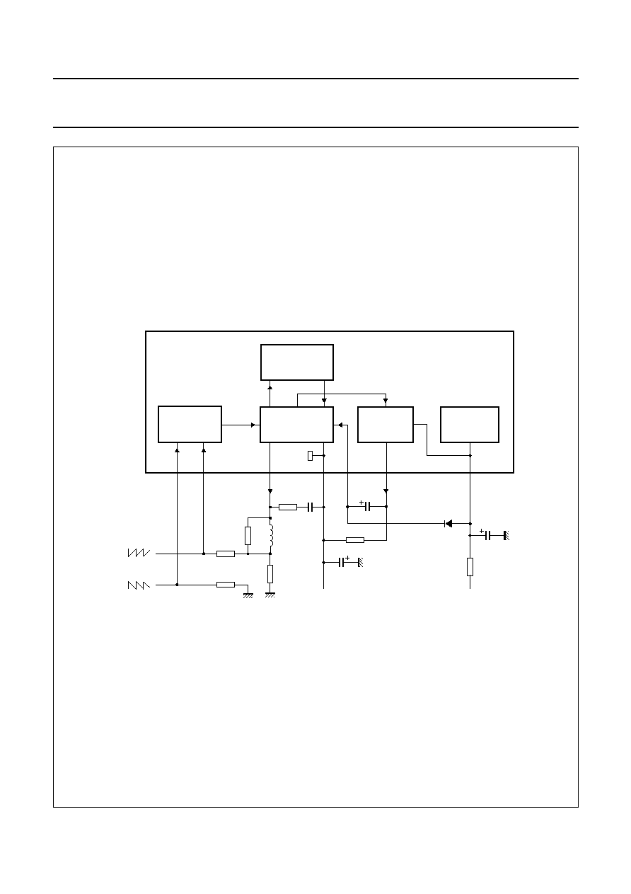
4
Philips Semiconductors
Product specification
Vertical deflection booster
TDA4864J; TDA4864AJ
handbook, full pagewidth
TDA4864AJ
DIFFERENTIAL
INPUT
STAGE
VERTICAL
OUTPUT
7
6
5
4
3
2
1
REFERENCE
CIRCUIT
FLYBACK
GENERATOR
VP1
VN
GND
deflection
coil
from
deflection controller
THERMAL
PROTECTION
VP3
V-OUT
R1
VP2
RS1
VP
CS1
CF
RP
R3
R2
D1
INN
INP
R6
R5
C1
C2
Fig.2 Block diagram of TDA4864AJ.

2003 Oct 31
5
Philips Semiconductors
Product specification
Vertical deflection booster
TDA4864J; TDA4864AJ
PINNING
SYMBOL
PIN
DESCRIPTION
TDA4864J
TDA4864AJ
V
P1
1
1
positive supply voltage 1
V
FB
2
-
flyback supply voltage
V
P3
-
2
flyback generator output
V
P2
3
3
supply voltage 2 for vertical output
GND
4
4
ground or negative supply voltage
V-OUT
5
5
vertical output
INN
6
6
inverted input of differential input stage
INP
7
7
non-inverted input of differential input stage
handbook, halfpage
VP1
VFB
VP2
GND
V-OUT
INN
INP
1
2
3
4
5
6
7
TDA4864J
XXXxxx
Fig.3 Pin configuration of TDA4864J.
handbook, halfpage
VP1
VP3
VP2
GND
V-OUT
INN
INP
1
2
3
4
5
6
7
TDA4864AJ
XXXxxx
Fig.4 Pin configuration of TDA4864AJ.

2003 Oct 31
6
Philips Semiconductors
Product specification
Vertical deflection booster
TDA4864J; TDA4864AJ
FUNCTIONAL DESCRIPTION
Both the TDA4864J and TDA4864AJ consist of a
differential input stage, a vertical output stage, a flyback
generator, a reference circuit and a thermal protection
circuit.
The TDA4864J operates with a separate flyback supply
voltage (see Fig.1) while the TDA4864AJ generates the
flyback voltage internally by doubling the supply voltage
(see Fig.2).
Differential input stage
The differential sawtooth input current signal (coming from
the deflection controller) is connected to the inputs
(inverted signal to pin INN and non-inverted signal to
pin INP). The vertical feedback signal is superimposed on
the inverted signal on pin INN.
Vertical output and thermal protection
The vertical output stage is a quasi-complementary
class-B amplifier with a high linearity.
The output stage is protected against thermal overshoots.
For a junction temperature T
j
> 150
∞
C this protection will
be activated and will reduce then the deflection current
(I
V-OUT
).
Flyback generator
The flyback generator supplies the vertical output stage
during flyback.
The TDA4864J is used with separate flyback supply
voltage to achieve a short flyback time with minimized
power dissipation.
The TDA4864AJ needs a capacitor C
F
between
pins V
P3
and V
P2
(see Fig.2). Capacitor C
F
is charged
during scan, using the external diode D1 and resistor R5.
During flyback the cathode of capacitor C
F
is connected to
the positive supply voltage and the flyback voltage is then
twice the supply voltage. For the TDA4864AJ the
resistor R6 in the positive supply line can be used to
reduce the power consumption.
In parallel with the deflection coil a damping resistor R
P
and an RC combination (R
S1
= 5.6
and C
S1
= 100 nF)
are needed. Furthermore, another additional
RC combination (R
S2
= 5.6
and C
S2
= 47 to 150 nF)
can be used to minimize the noise effect and the flyback
time (see Figs 9 and 10).

2003 Oct 31
7
Philips Semiconductors
Product specification
Vertical deflection booster
TDA4864J; TDA4864AJ
LIMITING VALUES
In accordance with the Absolute Maximum Rating System (IEC 60134); voltages referenced to pin GND; unless
otherwise specified.
Notes
1. Internally limited by thermal protection; will be activated for T
j
150
∞
C.
2. Equivalent to discharging a 200 pF capacitor through a 0
series resistor.
THERMAL CHARACTERISTICS
Note
1. To minimize the thermal resistance from mounting base to heatsink [R
th(mb-h)
] follow the recommended mounting
instruction: screw mounting preferred; torque = 40 Ncm; use heatsink compound; isolation plate increases R
th(mb-h)
.
SYMBOL
PARAMETER
CONDITIONS
MIN.
MAX.
UNIT
V
P1
supply voltage 1
-
40
V
V
P2
supply voltage 2
-
60
V
V
FB
flyback supply voltage of TDA4864J
-
60
V
V
P3
flyback generator output voltage of TDA4864AJ
0
V
P1
+ 3
V
V
i
input voltage on
pin INN
-
V
P1
V
pin INP
-
V
P1
V
V
o(V-OUT)
output voltage on pin V-OUT
-
62
V
I
P2
supply current 2
-
±
1.5
A
I
o(V-OUT)
output current on pin V-OUT
note 1
-
±
1.5
A
I
VFB
current during flyback of TDA4864J
-
±
1.5
A
I
VP3
current during flyback of TDA4864AJ
-
±
1.5
A
T
stg
storage temperature
-
25
+150
∞
C
T
amb
ambient temperature
-
20
+75
∞
C
T
j
junction temperature
note 1
-
150
∞
C
V
es
electrostatic discharge voltage on all pins
note 2
-
300
+
300
V
SYMBOL
PARAMETER
CONDITIONS
VALUE
UNIT
R
th(j-mb)
thermal resistance from junction to mounting base
note 1
6
K/W

2003 Oct 31
8
Philips Semiconductors
Product specification
Vertical deflection booster
TDA4864J; TDA4864AJ
CHARACTERISTICS
V
P1
= 25 V; T
amb
= 25
∞
C; voltages referenced to pin GND; unless otherwise specified.
Note
1. Deviation of the output slope at a constant input slope.
SYMBOL
PARAMETER
CONDITIONS
MIN.
TYP.
MAX.
UNIT
Supplies
V
P1
supply voltage 1
9
-
30
V
V
P2
supply voltage 2
V
P1
-
1
-
60
V
V
FB
flyback supply voltage of TDA4864J
V
P1
-
1
-
60
V
V
P3
flyback generator output voltage of TDA4864AJ
I
V-OUT
=
-
1.25 A
0
-
V
P1
+ 2.2 V
I
P1
supply current 1
during scan
-
6
10
mA
I
P2
quiescent supply current 2
I
V-OUT
= 0
-
25
60
mA
Differential input stage
V
i
input voltage on
pin INN
1.6
-
V
P1
-
0.5 V
pin INP
1.6
-
V
P1
-
0.5 V
I
q
input quiescent current on
pin INN
-
-
100
-
500
nA
pin INP
-
-
100
-
500
nA
Flyback generator
I
VFB
current during flyback of TDA4864J
-
-
±
1.5
A
I
VP3
current during flyback of TDA4864AJ
-
-
±
1.5
A
V
VP2-VFB
voltage drop during flyback of TDA4864J
reverse
I
V-OUT
=
-
1 A
-
-
1.5
-
V
I
V-OUT
=
-
1.25 A
-
-
2
-
V
forward
I
V-OUT
= 1 A
-
2.2
-
V
I
V-OUT
= 1.25 A
-
2.5
-
V
V
VP3-VP1
voltage drop during flyback of TDA4864AJ
reverse
I
V-OUT
=
-
1 A
-
-
1.5
-
V
I
V-OUT
=
-
1.25 A
-
-
2
-
V
forward
I
V-OUT
= 1 A
-
2.2
-
V
I
V-OUT
= 1.25 A
-
2.5
-
V
Vertical output stage; see Fig.5
I
V-OUT
vertical deflection output current
-
-
±
1.25
A
I
V-OUT(p-p)
vertical deflection output current
(peak-to-peak value)
-
-
2.5
A
V
o(sat)n
output saturation voltage to ground
I
V-OUT
= 1 A
-
1.4
1.7
V
I
V-OUT
= 1.25 A
-
1.8
2.3
V
V
o(sat)p
output saturation voltage to V
P2
I
V-OUT
= 1 A
-
2.3
-
2
-
V
I
V-OUT
= 1.25 A
-
2.8
-
2.3
-
V
LIN
non-linearity of output signal
note 1
-
-
1
%

2003 Oct 31
9
Philips Semiconductors
Product specification
Vertical deflection booster
TDA4864J; TDA4864AJ
handbook, full pagewidth
t
input signal
on pin INN
t
input signal
on pin INP
t
output voltage
on pin V-OUT
VFB
(1)
VP1
GND
t
deflection current
through the coil
MHB718
Fig.5 Timing diagram.
(1) V
FB
for TDA4864J; 2V
P1
for TDA4864AJ.

2003 Oct 31
10
Philips Semiconductors
Product specification
Vertical deflection booster
TDA4864J; TDA4864AJ
INTERNAL PIN CONFIGURATION
handbook, full pagewidth
7
6
1
3
2
4
5
GND
V-OUT
VFB
INP
INN
VP2
VP1
TDA4864J
Fig.6 Internal circuits of TDA4864J.
handbook, full pagewidth
7
6
1
3
2
4
5
GND
V-OUT
VP3
INP
INN
VP2
VP1
TDA4864AJ
Fig.7 Internal circuits of TDA4864AJ.

2003 Oct 31
11
Philips Semiconductors
Product specification
Vertical deflection booster
TDA4864J; TDA4864AJ
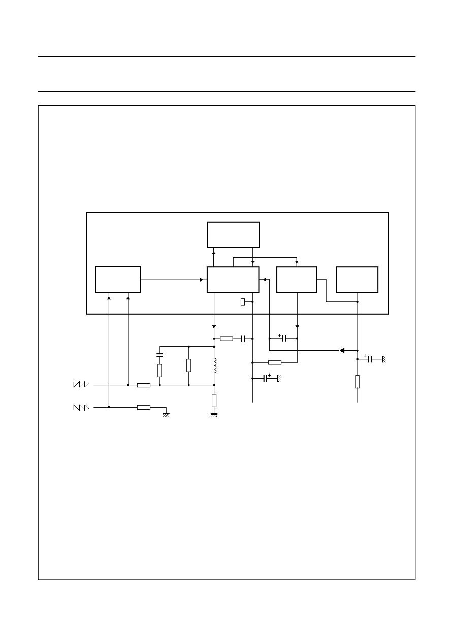
APPLICATION INFORMATION
handbook, full pagewidth
TDA4864J
22
µ
F
2
VF
5
VP
>
1 k
220 k
BC548
BC556
3.3 k
1N4448
2.2
guard output
HIGH = error
vertical
output
signal
Fig.8 Application circuit with TDA4864J for external guard signal generation.
handbook, full pagewidth
TDA4864J
470
µ
F
DIFFERENTIAL
INPUT
STAGE
VERTICAL
OUTPUT
7
6
5
4
3
2
1
REFERENCE
CIRCUIT
FLYBACK
GENERATOR
VP1
-
8 V
VN
GND
1.8 k
1
(1 W)
deflection
coil
4.3
5.6
100
nF
BYV27
from
deflection controller
+
50 V
THERMAL
PROTECTION
VFB
V-OUT
1.8 k
R1
470
µ
F
270
VF
VP2
RS1
470
µ
F
+
9 V
VP
CS1
RP
R3
R2
D1
INN
INP
5.6
RS2
CS2
(1)
Fig.9 Application circuit with TDA4864J.
Attention: the heatsink of the IC must be isolated against ground of the application (it is connected to pin GND).
(1) With C
S2
(typical value between 47 and 150 nF) the flyback time and the noise behaviour can be optimized.
2003 Oct 31
12
Philips Semiconductors
Product specification
Vertical deflection booster
TDA4864J; TDA4864AJ
handbook, full pagewidth
TDA4864AJ
470
µ
F
DIFFERENTIAL
INPUT
STAGE
VERTICAL
OUTPUT
7
6
5
4
3
2
1
REFERENCE
CIRCUIT
FLYBACK
GENERATOR
VP1
-
12.5 V
VN
GND
1.8 k
1
(1 W)
deflection
coil
3.9
(2 W)
5.6
100
nF
BYV27
from
deflection controller
THERMAL
PROTECTION
VP3
V-OUT
1.8 k
R1
100
µ
F
270
VP2
RS1
470
µ
F
+
12.5 V
VP
CS1
CF
RP
R3
R2
D1
INN
INP
5.6
RS2
CS2
(1)
R6
(3)
R5
(2)
240
(2 W)
Fig.10 Application circuit with TDA4864AJ.
Attention: the heatsink of the IC must be isolated against ground of the application (it is connected to pin GND).
(1) With C
S2
(typical value between 47 and 150 nF) the flyback time and the noise behaviour can be optimized.
(2) With R5 capacitor C
F
will be charged during scan and the value (typical value between 150 and 270
) depends on I
defl
, t
flb
and C
F
.
(3) R6 reduces the power dissipation of the IC. The maximum possible value depends on the application.
2003 Oct 31
13
Philips Semiconductors
Product specification
Vertical deflection booster
TDA4864J; TDA4864AJ
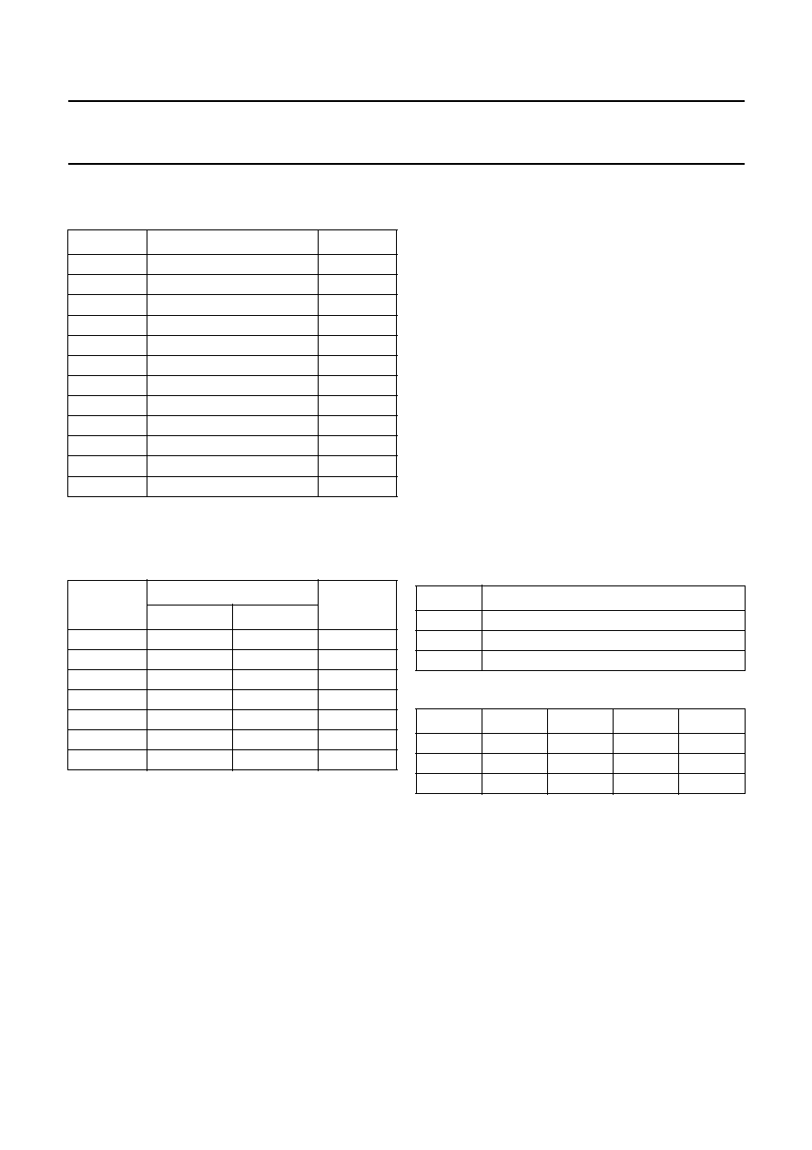
Example for both TDA4864J and TDA4864AJ
Table 1
Values given from application
Note
1. For TDA4864J only.
Table 2
Calculated values
V
P1
, V
N
and V
FB
are referenced to ground of application;
voltages are calculated with +10% tolerances.
Calculation formulae for supply voltages:
V
P1
=
-
V
o(sat)p
+ (R1 + R
deflcoil
)
◊
I
defl(max)
-
U'
L
+ U
D1
V
N
= V
o(sat)n
+ (R1 + R
deflcoil
)
◊
I
defl(max)
+ U'
L
where
U'
L
= L
deflcoil
◊
2I
defl(max)
◊
f
v
f
v
= vertical deflection frequency
U
D1
= forward voltage drop across D1.
Calculation formulae for power consumption:
where
P
IC
= power dissipation of the IC
P
tot
= total power dissipation
P
defl
= power dissipation of the deflection coil.
Calculation formulae for maximum required thermal
resistance for the heatsink at T
j(max)
= 110
∞
C:
Table 3
t
flb
as a function of V
FB
for TDA4864J
Table 4
t
flb
as a function of V
P1
and V
N
for TDA4864AJ
SYMBOL
VALUE
UNIT
I
defl(max)
0.71
A
L
deflcoil
6
mH
R
deflcoil
6
R
P
270
R1
1
R2
1.8
k
R3
1.8
k
V
FB
(1)
50
V
T
amb
60
∞
C
T
deflcoil
75
∞
C
R
th(j-mb)
6
K/W
R
th(mb-amb)
8
K/W
SYMBOL
VALUE
UNIT
TDA4864J
TDA4864AJ
V
P1
9
12.5
V
V
N
-
8
-
12.5
V
P
tot
3.2
4.4
W
P
defl
1.2
1.2
W
P
IC
2
3.2
W
R
th(tot)
14
14
K/W
T
j(max)
88
105
∞
C
t
flb
(
µ
s)
V
FB
(V)
350
30
250
40
210
50
t
flb
(
µ
s)
V
P1
(V)
V
N
(V)
P
IC
(W)
R6 (
)
360
10
-
10
2.5
1
290
12.5
-
12.5
3.2
3.9
240
15
-
15
3.9
6.8
P
IC
P
tot
P
defl
≠
=
P
tot
V
P1
U
D1
≠
(
)
I
defl(max)
4
--------------------
V
N
I
defl(max)
4
--------------------
◊
+
◊
=
V
P1
V
N
≠
(
)
0.01 A
0.2 W
+
◊
+
P
defl
R
deflcoil
R1
+
3
--------------------------------
I
defl(max)
2
◊
=
R
th(mb-amb)
T
j(max)
T
amb
≠
P
IC
-----------------------------------
R
th(j-mb)
≠
19 K/W (max.)
=
=

2003 Oct 31
14
Philips Semiconductors
Product specification
Vertical deflection booster
TDA4864J; TDA4864AJ
PACKAGE OUTLINE
REFERENCES
OUTLINE
VERSION
EUROPEAN
PROJECTION
ISSUE DATE
IEC
JEDEC
JEITA
DIMENSIONS (mm are the original dimensions)
Notes
1. Plastic or metal protrusions of 0.25 mm maximum per side are not included.
2. Plastic surface within circle area D1 may protrude 0.04 mm maximum.
SOT524-1
0
10 mm
5
scale
w
M
bp
Dh
q1
Z
1
7
e
e1
m
e2
x
A2
non-concave
D1
D
P
k
q2
L3
L2
L
Q
c
E
00-07-03
03-03-12
DBS7P: plastic DIL-bent-SIL power package; 7 leads (lead length 12/11 mm); exposed die pad
SOT524-1
view B: mounting base side
B
UNIT
bp
L1
c
D
(1)
Dh
L
q2
mm
2.7
2.3
A2
(2)
0.80
0.65
0.58
0.48
13.2
12.8
D1
(2)
6.2
5.8
3.5
Eh
3.5
e
2.54
e1
1.27
e2
5.08
4.85
Q
E
(1)
14.7
14.3
Z
(1)
2.92
2.37
11.4
10.0
L2
6.7
5.5
L3
4.5
3.7
3.4
3.1
1.15
0.85
q
17.5
16.3
q1
2.8
m
0.8
v
3.8
3.6
3
2
12.4
11.0
P
k
0.02
x
0.3
w
Eh
L1
q
v
M

2003 Oct 31
15
Philips Semiconductors
Product specification
Vertical deflection booster
TDA4864J; TDA4864AJ
SOLDERING
Introduction to soldering through-hole mount
packages
This text gives a brief insight to wave, dip and manual
soldering. A more in-depth account of soldering ICs can be
found in our
"Data Handbook IC26; Integrated Circuit
Packages" (document order number 9398 652 90011).
Wave soldering is the preferred method for mounting of
through-hole mount IC packages on a printed-circuit
board.
Soldering by dipping or by solder wave
Driven by legislation and environmental forces the
worldwide use of lead-free solder pastes is increasing.
Typical dwell time of the leads in the wave ranges from
3 to 4 seconds at 250
∞
C or 265
∞
C, depending on solder
material applied, SnPb or Pb-free respectively.
The total contact time of successive solder waves must not
exceed 5 seconds.
The device may be mounted up to the seating plane, but
the temperature of the plastic body must not exceed the
specified maximum storage temperature (T
stg(max)
). If the
printed-circuit board has been pre-heated, forced cooling
may be necessary immediately after soldering to keep the
temperature within the permissible limit.
Manual soldering
Apply the soldering iron (24 V or less) to the lead(s) of the
package, either below the seating plane or not more than
2 mm above it. If the temperature of the soldering iron bit
is less than 300
∞
C it may remain in contact for up to
10 seconds. If the bit temperature is between
300 and 400
∞
C, contact may be up to 5 seconds.
Suitability of through-hole mount IC packages for dipping and wave soldering methods
Notes
1. For SDIP packages, the longitudinal axis must be parallel to the transport direction of the printed-circuit board.
2. For PMFP packages hot bar soldering or manual soldering is suitable.
PACKAGE
SOLDERING METHOD
DIPPING
WAVE
DBS, DIP, HDIP, RDBS, SDIP, SIL
suitable
suitable
(1)
PMFP
(2)
-
not suitable

2003 Oct 31
16
Philips Semiconductors
Product specification
Vertical deflection booster
TDA4864J; TDA4864AJ
DATA SHEET STATUS
Notes
1. Please consult the most recently issued data sheet before initiating or completing a design.
2. The product status of the device(s) described in this data sheet may have changed since this data sheet was
published. The latest information is available on the Internet at URL http://www.semiconductors.philips.com.
3. For data sheets describing multiple type numbers, the highest-level product status determines the data sheet status.
LEVEL
DATA SHEET
STATUS
(1)
PRODUCT
STATUS
(2)(3)
DEFINITION
I
Objective data
Development
This data sheet contains data from the objective specification for product
development. Philips Semiconductors reserves the right to change the
specification in any manner without notice.
II
Preliminary data Qualification
This data sheet contains data from the preliminary specification.
Supplementary data will be published at a later date. Philips
Semiconductors reserves the right to change the specification without
notice, in order to improve the design and supply the best possible
product.
III
Product data
Production
This data sheet contains data from the product specification. Philips
Semiconductors reserves the right to make changes at any time in order
to improve the design, manufacturing and supply. Relevant changes will
be communicated via a Customer Product/Process Change Notification
(CPCN).
DEFINITIONS
Short-form specification
The data in a short-form
specification is extracted from a full data sheet with the
same type number and title. For detailed information see
the relevant data sheet or data handbook.
Limiting values definition
Limiting values given are in
accordance with the Absolute Maximum Rating System
(IEC 60134). Stress above one or more of the limiting
values may cause permanent damage to the device.
These are stress ratings only and operation of the device
at these or at any other conditions above those given in the
Characteristics sections of the specification is not implied.
Exposure to limiting values for extended periods may
affect device reliability.
Application information
Applications that are
described herein for any of these products are for
illustrative purposes only. Philips Semiconductors make
no representation or warranty that such applications will be
suitable for the specified use without further testing or
modification.
DISCLAIMERS
Life support applications
These products are not
designed for use in life support appliances, devices, or
systems where malfunction of these products can
reasonably be expected to result in personal injury. Philips
Semiconductors customers using or selling these products
for use in such applications do so at their own risk and
agree to fully indemnify Philips Semiconductors for any
damages resulting from such application.
Right to make changes
Philips Semiconductors
reserves the right to make changes in the products -
including circuits, standard cells, and/or software -
described or contained herein in order to improve design
and/or performance. When the product is in full production
(status `Production'), relevant changes will be
communicated via a Customer Product/Process Change
Notification (CPCN). Philips Semiconductors assumes no
responsibility or liability for the use of any of these
products, conveys no licence or title under any patent,
copyright, or mask work right to these products, and
makes no representations or warranties that these
products are free from patent, copyright, or mask work
right infringement, unless otherwise specified.