Document Outline
- FEATURES
- APPLICATIONS
- GENERAL DESCRIPTION
- QUICK REFERENCE DATA
- ORDERING INFORMATION
- BLOCK DIAGRAM
- PINNING
- FUNCTIONAL DESCRIPTION
- Power supply
- Supply voltage supervisor (VDD )
- Clock circuitry
- I/O circuitry
- Logic circuitry
- State diagram
- Fault detection
- LIMITING VALUES
- HANDLING
- THERMAL CHARACTERISTICS
- CHARACTERISTICS
- APPLICATION INFORMATION
- PACKAGE OUTLINES
- SOLDERING
- DEFINITIONS
- LIFE SUPPORT APPLICATIONS

DATA SHEET
Product specification
Supersedes data of 1997 Mar 13
File under Integrated Circuits, IC02
1997 Nov 04
INTEGRATED CIRCUITS
TDA8002
IC card interface

1997 Nov 04
2
Philips Semiconductors
Product specification
IC card interface
TDA8002
FEATURES
∑
Single supply voltage interface (3.3 or 5 V environment)
∑
Low-power sleep mode
∑
Three specific protected half-duplex bidirectional
buffered I/O lines
∑
V
CC
regulation (5 V
±
5%, I
CC
<65 mA at V
DD
= 5 V, with
controlled rise and fall times
∑
Thermal and short-circuit protections with current
limitations
∑
Automatic ISO 7816 activation and deactivation
sequences
∑
Enhanced ESD protections on card side (>6 kV)
∑
Clock generation for the card up to 12 MHz with
synchronous frequency changes
∑
Clock generation up to 20 MHz (auxiliary clock)
∑
Synchronous and asynchronous cards (memory and
smart cards)
∑
ISO 7816, GSM11.11 compatibility and EMV (Europay,
Mastercard, Visa) compliant
∑
Step-up converter for V
CC
generation
∑
Supply supervisor for spikes elimination and emergency
deactivation.
APPLICATIONS
∑
IC card readers for:
≠ GSM applications
≠ banking
≠ electronic payment
≠ identification
≠ Pay TV
≠ road tolling.
GENERAL DESCRIPTION
The TDA8002 is a complete low-power, analog interface
for asynchronous and synchronous cards. It can be placed
between the card and the microcontroller. It performs all
supply, protection and control functions. It is directly
compatible with ISO 7816, GSM11.11 and EMV
specifications.
QUICK REFERENCE DATA
SYMBOL
PARAMETER
CONDITIONS
MIN.
TYP.
MAX.
UNIT
Supply
V
DDA
analog supply voltage
3.0
5
6.5
V
I
DD
supply current
sleep mode
-
-
150
µ
A
idle mode; f
CLK
= 2.5 MHz;
f
CLKOUT
= 10 MHz; V
DD
= 5 V
-
-
6
mA
active mode; f
CLK
= 2.5 MHz;
f
CLKOUT
= 10 MHz; V
DD
= 5 V
-
-
9
mA
active mode; f
CLK
= 2.5 MHz;
f
CLKOUT
= 10 MHz; V
DD
= 3 V
-
-
12
mA
Card supply
V
CC(O)
output voltage
DC load <65 mA
4.75
-
5.25
V
I
CC(O)
output current
V
CC
short-circuited to GND
-
-
100
mA
General
f
CLK
card clock frequency
0
-
12
MHz
T
de
deactivation cycle time
60
80
100
µ
s
P
tot
continuous total power dissipation
TDA8002AT; TDA8002BT
T
amb
=
-
25 to +85
∞
C
-
-
0.56
W
TDA8002G
T
amb
=
-
25 to +85
∞
C
-
-
0.46
W
T
amb
operating ambient temperature
-
25
-
+85
∞
C

1997 Nov 04
3
Philips Semiconductors
Product specification
IC card interface
TDA8002
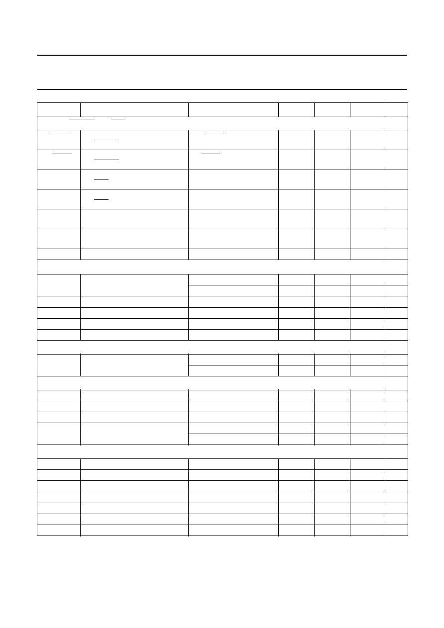
ORDERING INFORMATION
Notes
1. The /3 or /5 suffix indicates the voltage supervisor option.
2. The /3 version can be used with a 3 or 5 V power supply environment (see Chapter "Functional description").
3. The /5 version can be used with a 5 V power supply environment.
TYPE NUMBER
(1)
PACKAGE
MARKING
NAME
DESCRIPTION
VERSION
TDA8002AT/3/C2
(2)
TDA8002AT/3
SO28
plastic small outline package; 28 leads;
body width 7.5 mm
SOT136-1
TDA8002AT/5/C2
(3)
TDA8002AT/5
TDA8002BT/3/C2
(2)
TDA8002BT/3
TDA8002BT/5/C2
(3)
TDA8002BT/5
TDA8002G/3/C2
(2)
80023
LQFP32 plastic low profile quad flat package; 32 leads;
body 5
◊
5
◊
1.4 mm
SOT401-1
TDA8002G/5/C2
(3)
80025

1997 Nov 04
4
Philips Semiconductors
Product specification
IC card interface
TDA8002
BLOCK DIAGRAM
Fig.1 Block diagram (TDA8002G).
All capacitors are mandatory.
handbook, full pagewidth
MGE730
100 nF
100 nF
100 nF
100 nF
100
nF
I/O
TRANSCEIVER
I/O
TRANSCEIVER
I/O
TRANSCEIVER
THERMAL
PROTECTION
VCC
GENERATOR
RST
BUFFER
CLOCK
BUFFER
SEQUENCER
CLOCK
CIRCUITRY
OSCILLATOR
HORSEQ
INTERNAL OSCILLATOR
fINT
STEP-UP CONVERTER
INTERNAL
REFERENCE
VOLTAGE SENSE
SUPPLY
EN2
PVCC
EN5
EN4
EN3
CLK
EN1
CLKUP
ALARM
VREF
28
VDDD
13
VDDA
14
12
S1
S2
15 VUP
23
VCC
22
RST
PRES
19
18
PRES
21
CLK
20
17
16
AUX1
AUX2
I/O
10
29
11
DGND1 DGND2
AGND
32
2
1
I/OUC
AUX2UC
AUX1UC
31
30
9
8
5
7
6
27
24
25
26
XTAL2
XTAL1
CLKOUT
STROBE
CLKSEL
CLKDIV2
CLKDIV1
MODE
CMDVCC
RSTIN
OFF
3
4
ALARM
ALARM
TDA8002G

1997 Nov 04
5
Philips Semiconductors
Product specification
IC card interface
TDA8002
PINNING
SYMBOL
PIN
I/O
DESCRIPTION
TYPE A
TYPE B
TYPE G
XTAL1
1
1
30
I/O
crystal connection or input for external clock
XTAL2
2
2
31
I/O
crystal connection
I/OUC
3
3
32
I/O
data I/O line to and from microcontroller
AUX1UC
4
4
1
I/O
auxiliary line to and from microcontroller for synchronous
applications
AUX2UC
5
-
2
I/O
auxiliary line to and from microcontroller for synchronous
applications
ALARM
-
5
3
O
open drain NMOS reset output for microcontroller (active LOW)
ALARM
6
6
4
O
open drain PMOS reset output for microcontroller (active
HIGH)
CLKSEL
7
7
5
I
control input signal for CLK (LOW = XTAL oscillator;
HIGH = STROBE input)
CLKDIV1
8
8
6
I
control input with CLKDIV2 for choosing CLK frequency
CLKDIV2
9
9
7
I
control input with CLKDIV1 for choosing CLK frequency
STROBE
10
10
8
I
external clock input for synchronous applications
CLKOUT
11
11
9
O
clock output (see Table 1)
DGND1
12
12
10
supply
digital ground 1
AGND
13
13
11
supply
analog ground
S2
14
14
12
I/O
capacitance connection for voltage doubler
V
DDA
15
15
13
supply
analog supply voltage
S1
16
16
14
I/O
capacitance connection for voltage doubler
VUP
17
17
15
I/O
output of voltage doubler (connect to 100 nF)
I/O
18
18
16
I/O
data I/O line to and from card
AUX2
19
-
17
I/O
auxiliary I/O line to and from card
PRES
20
19
18
I
active LOW card input presence contact
PRES
-
20
19
I
active HIGH card input presence contact
AUX1
21
21
20
I/O
auxiliary I/O line to and from card
CLK
22
22
21
O
clock to card output (C3) (see Table 1)
RST
23
23
22
O
card reset output (C2)
V
CC
24
24
23
O
supply for card (C1) (decouple with 100 nF)
CMDVCC
25
25
24
I
active LOW start activation sequence input from
microcontroller
RSTIN
26
26
25
I
card reset input from microcontroller
OFF
27
27
26
O
open drain NMOS interrupt output to microcontroller (active
LOW)
MODE
28
28
27
I
operating mode selection input (HIGH = normal; LOW = sleep)
V
DDD
-
-
28
supply
digital supply voltage
DGND2
-
-
29
supply
digital ground 2

1997 Nov 04
6
Philips Semiconductors
Product specification
IC card interface
TDA8002
Fig.2 Pin configuration (TDA8002A).
handbook, halfpage
XTAL1
XTAL2
I/OUC
AUX1UC
AUX2UC
ALARM
CLKSEL
CLKDIV1
CLKDIV2
STROBE
CLKOUT
DGND1
AGND
S2
MODE
RSTIN
RST
CLK
VCC
AUX1
AUX2
I/O
VUP
S1
VDDA
1
2
3
4
5
6
7
8
9
10
11
12
13
28
27
26
25
24
23
22
21
20
19
18
17
16
15
14
TDA8002A
MGE731
OFF
CMDVCC
PRES
Fig.3 Pin configuration (TDA8002B).
handbook, halfpage
XTAL1
XTAL2
I/OUC
AUX1UC
ALARM
CLKSEL
CLKDIV1
CLKDIV2
STROBE
CLKOUT
DGND1
AGND
S2
MODE
RSTIN
RST
CLK
VCC
AUX1
PRES
I/O
VUP
S1
VDDA
1
2
3
4
5
6
7
8
9
10
11
12
13
28
27
26
25
24
23
22
21
20
19
18
17
16
15
14
TDA8002B
MGE732
OFF
CMDVCC
PRES
ALARM
Fig.4 Pin configuration (TDA8002G).
handbook, full pagewidth
TDA8002G
MGE733
1
2
3
4
5
6
7
8
24
23
22
21
20
19
18
17
9
10
11
12
13
14
15
16
32
31
30
29
28
27
26
25
AUX1UC
AUX2UC
ALARM
CLKSEL
CLKDIV1
CLKDIV2
STROBE
CLKOUT
DGND1
AGND
S2
S1
VUP
I/O
AUX2
AUX1
RSTIN
MODE
V
DDD
DGND2
XTAL1
XTAL2
I/OUC
RST
CLK
VCC
PRES
V
DDA
ALARM
PRES
CMDVCC
OFF

1997 Nov 04
7
Philips Semiconductors
Product specification
IC card interface
TDA8002
FUNCTIONAL DESCRIPTION
Power supply
The supply pins for the chip are V
DDA
, V
DDD
, AGND,
DGND1 and DGND2. V
DDA
and V
DDD
(i.e. V
DD
) should be
in the range of 3.0 to 6.5 V. All card contacts remain
inactive during power-up or power-down.
On power-up, the logic is reset by an internal signal.
The sequencer is not activated until V
DD
reaches
V
th2
+ V
hys2
(see Fig.5). When V
DD
falls below V
th2
, an
automatic deactivation sequence of the contacts is
performed.
Supply voltage supervisor (V
DD
)
This block surveys the V
DD
supply. A defined reset pulse
of 10 ms minimum (t
W
) can be retriggered and is delivered
on the ALARM outputs during power-up or power-down of
V
DD
(see Fig.5). This signal is also used for eliminating the
spikes on card contacts during power-up or power-down.
When V
DD
reaches V
th2
+ V
hys2
, an internal delay is
started. The ALARM outputs are active until this delay has
expired. When V
DD
falls below V
th2
, ALARM is activated
and a deactivation sequence of the contacts is performed.
For 3 V supply, the supervisor option must be chosen at
3 V. For 5 V supply, both options (3 or 5 V) may be chosen
depending on the application.
Clock circuitry
The TDA8002 supports both synchronous and
asynchronous cards (I
2
C-bus memories requiring an
acknowledge signal from the master are not supported).
There are three methods to clock the circuitry:
∑
Apply a clock signal to pin STROBE
∑
Use of an internal RC oscillator
∑
Use of a quartz oscillator which should be connected
between pins XTAL1 and XTAL2.
When CLKSEL is HIGH, the clock should be applied on the
STROBE pin, and when CLKSEL is LOW, one of the
internal oscillators is used.
When an internal clock is used, the clock output is
available on pin CLKOUT. The RC oscillator is selected by
making CLKDIV1 HIGH and CLKDIV2 LOW. The clock
output to the card is available on pin CLK. The frequency
of the card clock can be the input frequency divided by
2 or 4, STOP LOW or 1.25 MHz, depending on the states
of CLKDIV1 or CLKDIV2 (see Table 1).
Do not change CLKSEL during activation. When in
low-power (sleep) mode, the internal oscillator frequency
which is available on pin CLKOUT is lowered to
approximately 16 kHz for power-economy purposes.
Fig.5 Alarm as a function of V
DD
(pulse width 10 ms).
handbook, full pagewidth
MGE734
VDD
tW
tW
Vth2
+
Vhys2
Vth2
ALARM
ALARM

1997 Nov 04
8
Philips Semiconductors
Product specification
IC card interface
TDA8002
Table 1
Clock circuitry definition
Notes
1. X = don't care.
2. In low-power mode.
3. f
int
= 32 kHz in low-power mode.
MODE
CLKSEL
CLKDIV1
CLKDIV2
FREQUENCY
OF CLK
FREQUENCY
OF CLKOUT
HIGH
LOW
HIGH
LOW
1
/
2
f
int
1
/
2
f
int
HIGH
LOW
LOW
LOW
1
/
4
f
xtal
f
xtal
HIGH
LOW
LOW
HIGH
1
/
2
f
xtal
f
xtal
HIGH
LOW
HIGH
HIGH
STOP LOW
f
xtal
HIGH
HIGH
X
(1)
X
(1)
STROBE
f
xtal
LOW
(2)
X
(1)
X
(1)
X
(1)
STOP LOW
1
/
2
f
int
(3)
I/O circuitry
The three I/O transceivers are identical. The state is HIGH
for all I/O pins (i.e. I/O, I/OUC, AUX1, AUX1UC, AUX2 and
AUX2UC). Pin I/O is referenced to V
CC
and pin I/OUC to
V
DD
, thus ensuring proper operation in case V
CC
V
DD
.
The first side on which a falling edge is detected becomes
a master (input). An anti-latch circuitry first disables the
detection of the falling edge on the other side, which
becomes slave (output).
After a delay time t
d
(about 50 ns), the logic 0 present on
the master side is transferred on the slave side.
When the input is back to HIGH level, a current booster is
turned on during the delay t
d
on the output side and then
both sides are back to their idle state, ready to detect the
next logic 0 on any side.
In case of a conflict, both lines may remain LOW until the
software enables the lines to be HIGH. The anti-latch
circuitry ensures that the lines do not remain LOW if both
sides return HIGH, regardless of the prior conditions.
The maximum frequency on the lines is approximately
1 MHz.
Fig.6 Master and slave signals.
handbook, full pagewidth
td
MGD703
td
td
I/O
I/OUC
conflict
idle

1997 Nov 04
9
Philips Semiconductors
Product specification
IC card interface
TDA8002
Logic circuitry
After power-up, the circuit has six possible states of
operation. Table 1 shows the sequence of these states.
I
DLE MODE
After reset, the circuit enters the idle mode.
A minimum number of functions in the circuit are active
while waiting for the microcontroller to start a session:
∑
All card contacts are inactive
∑
I/OUC, AUX1UC and AUX2UC are high-impedance
∑
Oscillator XTAL runs, delivering CLKOUT
∑
Voltage supervisor is active.
L
OW
-
POWER
(
SLEEP
)
MODE
When pin MODE goes LOW, the circuit enters the
low-power (sleep) mode. As long as pin MODE is LOW, no
activation is possible.
If pin MODE goes LOW in the active mode, a normal
deactivation sequence is performed before entering
low-power mode. When pin MODE goes HIGH, the circuit
enters normal operation after a delay of at least 6 ms
(96 cycles of CLKOUT). During this time the CLKOUT
remains at 16 kHz.
∑
All card contacts are inactive
∑
Oscillator XTAL does not run
∑
The V
DD
supervisor, ALARM output, card presence
detection and OFF output remain functional
∑
Internal oscillator is slowed to 32 kHz, CLKOUT
providing 16 kHz.
A
CTIVE MODE
When the activation sequence is completed, the TDA8002
will be in the active mode. Data is exchanged between the
card and the microcontroller via the I/O lines.
State diagram
Fig.7 State diagram.
handbook, full pagewidth
MGE735
POWER
OFF
ACTIVE
MODE
LOW-POWER
MODE
IDLE
MODE
FAULT
ACTIVATION
DEACTIVATION

1997 Nov 04
10
Philips Semiconductors
Product specification
IC card interface
TDA8002
A
CTIVATION SEQUENCE
From idle mode, the circuit enters the activation mode
when the microcontroller sets the CMDVCC line LOW or
sets the MODE line HIGH when the CMDVCC line is
already LOW. The internal circuitry is then activated, the
internal clock is activated and an activation sequence is
executed. When RST is enabled, it becomes the inverse of
RSTIN.
Figures 8 to 10 illustrate the activation sequence as
described below:
1. Step-up converter is started (t
1
t
0
)
2. V
CC
rises from 0 to 5 V (t
2
= t
1
+ 1
1
/
2
T)
3. I/O, AUX1, AUX2 are enabled and CLK is enabled
(t
3
= t
1
+ 4T); a special circuitry ensures that I/O
remains below V
CC
during falling slope of V
CC
4. CLK is set by setting RSTIN to HIGH (t
4
)
5. RST is enabled (t
5
= t
1
+ 7T); after t
5
, RSTIN has no
further action on CLK, but is only controlling RST.
Fig.8 Activation sequence using RSTIN and CMDVCC.
handbook, full pagewidth
MGE736
OSC_INT/64
CMDVCC
VUP
VCC
I/O
CLK
RSTIN
RST
high - Z
tact
t0
t1
t2
t3
t4
t5
T = 25
µ
s

1997 Nov 04
11
Philips Semiconductors
Product specification
IC card interface
TDA8002
Fig.9 Activation sequence using CMDVCC, CLKDIV1 and CLKDIV2 signals to enable CLK.
handbook, full pagewidth
MGE737
OSC_INT/64
CMDVCC
VUP
VCC
I/O
CLK
RSTIN
RST
high - Z
tact
t0
t1
t2
t3
CLKDIV1
CLKDIV2
Fig.10 Activation sequence for synchronous application.
handbook, full pagewidth
MGE738
OSC_INT/64
VCC
I/O
RSTIN
RST
STROBE
high - Z
tact
CMDVCC
PRES, OFF

1997 Nov 04
12
Philips Semiconductors
Product specification
IC card interface
TDA8002
D
EACTIVATION SEQUENCE
When a session is completed, the microcontroller sets the
CMDVCC line to HIGH state or MODE line to LOW state.
The circuit then executes an automatic deactivation
sequence by counting the sequencer down and ends in
idle mode.
Figures 11 and 12 illustrate the deactivation sequence as
described below:
1. RST goes LOW (t
11
t
10
)
2. CLK is stopped (t
12
= t
11
+
1
/
2
T)
3. I/O, AUX1, AUX2 are outputs into high-impedance
state (t
13
= t
11
+ T)
4. V
CC
falls to zero (t
14
= t
11
+ 1
1
/
2
T); a special circuitry
ensures that I/O remains below V
CC
during falling
slope of V
CC
5. VUP falls (t
15
= t
11
+ 5T).
Fig.11 Deactivation sequence.
handbook, full pagewidth
MGE739
CMDVCC
VUP
OSC_INT/64
VCC
I/O
CLK
RSTIN
RST
high - Z
tde
t10
t11
t12
t13
t14
t15

1997 Nov 04
13
Philips Semiconductors
Product specification
IC card interface
TDA8002
Fault detection
The following fault conditions are monitored by the circuit:
∑
Short-circuit or high current on V
CC
∑
Removing card during transaction
∑
V
DD
dropping
∑
Overheating.
When one or more of these faults are detected, the circuit
pulls the interrupt line OFF to its active LOW state and a
deactivation sequence is initiated. In case the card is
present the interrupt line OFF is set to HIGH when the
microcontroller has reset the CMDVCC line HIGH (after
completion of the deactivation sequence). In case the card
is not present OFF remains LOW.
Fig.12 Emergency deactivation sequence.
handbook, full pagewidth
MGE740
I/O
CLK
RST
high - Z
tde
OSC_INT/64
OFF
PRES
VCC
t10
t11
t12
t13
t14

1997 Nov 04
14
Philips Semiconductors
Product specification
IC card interface
TDA8002
LIMITING VALUES
In accordance with the Absolute Maximum Rating System (IEC 134); note 1.
Note
1. Stress beyond these levels may cause permanent damage to the device. This is a stress rating only and functional
operation of the device under this condition is not implied.
HANDLING
Every pin withstands the ESD test according to MIL-STD-883C class 3 for card contacts, class 2 for the remaining.
Method 3015 (HBM 1500
, 100 pF) 3 positive pulses and 3 negative pulses on each pin referenced to ground.
THERMAL CHARACTERISTICS
SYMBOL
PARAMETER
CONDITIONS
MIN.
MAX.
UNIT
V
DD
supply voltage
-
0.3
+6.5
V
V
i(CMOS)
voltage on CMOS pins
XTAL1, XTAL2, ALARM, ALARM,
MODE, RSTIN, CLKSEL, AUX2UC,
AUX1UC, CLKDIV1, CLKDIV2,
CLKOUT, STROBE, CMDVCC and
OFF
-
0.3
+6.5
V
V
i(card)
voltage on card contact pins
I/O, AUX2, PRES, PRES, AUX1,
CLK, RST and V
CC
-
0.3
+6.5
V
V
es
electrostatic handling
on pins I/O, RST, V
CC
, CLK, AUX1,
AUX2, PRES and PRES
-
6
+6
kV
on all other pins
-
2
+2
kV
T
stg
storage temperature
-
55
+125
∞
C
P
tot
continuous total power dissipation
TDA8002T
T
amb
=
-
25 to +85
∞
C
-
0.56
W
TDA8002G
T
amb
=
-
25 to +85
∞
C
-
0.46
W
T
amb
operating ambient temperature
-
25
+85
∞
C
T
j
junction temperature
-
150
∞
C
SYMBOL
PARAMETER
VALUE
UNIT
R
th(j-a)
thermal resistance from junction to ambient in free air
SOT136-1
70
K/W
SOT401-1
91
K/W

1997 Nov 04
15
Philips Semiconductors
Product specification
IC card interface
TDA8002
CHARACTERISTICS
V
DD
= 5 V; T
amb
= 25
∞
C; f
xtal
= 10 MHz; unless otherwise specified.
SYMBOL
PARAMETER
CONDITIONS
MIN.
TYP.
MAX.
UNIT
Supply
V
DD
positive supply voltage
option 5 V power supply
(TDA8002xx/5)
4.5
5
6.5
V
option 3.3 V or 5 V power
supply (TDA8002xx/3)
3
5
6.5
V
I
DD(sl)
supply current
sleep mode; V
DD
= 5 V
-
-
200
µ
A
I
DD(idle)
supply current
idle mode; V
DD
= 5 V;
f
CLK
= 2.5 MHz;
f
CLKOUT
= 10 MHz
-
-
6
mA
I
DD(active)
supply current
active mode
V
DD
= 5 V;
f
CLK
= 2.5 MHz;
f
CLKOUT
= 10 MHz
-
-
9
mA
V
DD
= 3.3 V;
f
CLK
= 2.5 MHz;
f
CLKOUT
= 10 MHz
-
-
12
mA
V
th2
threshold voltage on V
DD
for
voltage supervisor
falling
option 5 V power supply
(TDA8002xx/5)
3.9
4.05
4.2
V
option 3.3 V or 5 V power
supply (TDA8002xx/3)
2.6
2.7
2.8
V
rising
option 5 V power supply
(TDA8002xx/5)
4
4.2
4.4
V
option 3.3 or 5 V power
supply (TDA8002xx/3)
2.7
2.85
2.99
V
V
hys2
hysteresis on V
th2
100
150
200
mV
C
ARD SUPPLY
V
CC(O)(idle)
output voltage
idle mode
-
-
0.4
V
V
CC(O)(active)
output voltage
active mode
I
CC
< 20 mA: DC load
with 3 V < V
DD
< 3.3 V
4.75
-
5.25
V
I
CC
< 65 mA: DC load
with 3.3 V < V
DD
< 6.5 V
4.75
-
5.25
V
I
CC
= 40 mA: AC load
4.6
-
5.4
V
I
CC(O)
output current
V
CC(O)
= from 0 to 5 V
-
-
65
mA
V
CC
short-circuited to
ground
-
-
100
mA
SR
slew rate
rising or falling slope
0.12
0.17
0.22
V/
µ
s
1997 Nov 04
16
Philips Semiconductors
Product specification
IC card interface
TDA8002
Crystal connections (XTAL1 and XTAL2)
C
ext
external capacitors
note 1
-
15
-
pF
f
xtal
resonance frequency
note 2
2
-
24
MHz
Data lines
G
ENERAL
t
edge
delay between falling edge of
I/O, AUX1, AUX2 and I/OUC,
AUX1UC, AUX2UC
-
200
-
ns
delay between falling edge of
I/OUC, AUX1UC, AUX2UC and
I/O, AUX1, AUX2
-
200
-
ns
t
r
, t
f
rise and fall times
C
i
= C
o
= 30 pF
-
-
0.5
µ
s
D
ATA LINES
I/O, AUX1
AND
AUX2
V
OH(I/O)
HIGH-level output voltage on
data lines
I
OH
=
-
20
µ
A
V
CC
-
0.5
-
V
CC
+ 0.1 V
I
OH
=
-
100
µ
A
3.5
-
-
V
V
OL(I/O)
LOW-level output voltage on
data lines
I
I/O
= 1 mA
-
-
300
mV
V
IH(I/O)
HIGH-level input voltage on data
lines
1.8
-
V
CC
V
V
IL(I/O)
LOW-level input voltage on data
lines
0
-
0.8
V
V
I/O(idle)
voltage on data lines outside a
session
-
-
0.4
V
R
pu
internal pull-up resistance
between data lines and V
CC
8
10
12
k
I
edge
current from data lines when
active pull-up is active
-
1
-
mA
I
IL(I/O)
LOW-level input current on data
lines
V
IL
= 0.4 V
-
-
-
600
µ
A
I
IH(I/O)
HIGH-level input current on data
lines
V
IH
= V
CC
-
-
10
µ
A
D
ATA LINES
I/OUC, AUX1UC
AND
AUX2UC
V
OH(I/OUC)
HIGH-level output voltage on
data lines
I
OH
=
-
20
µ
A
V
DD
-
1
-
V
DD
+ 0.2 V
V
OL(I/OUC)
LOW-level output voltage on
data lines
I
I/OUC
= 1 mA
-
-
300
mV
V
IH(I/OUC)
HIGH-level input voltage on data
lines
0.7V
DD
-
V
DD
V
V
IL(I/OUC)
LOW-level input voltage on data
lines
0
-
0.3V
DD
V
Z
I/OUC(idle)
impedance on data lines outside
a session
10
-
-
M
SYMBOL
PARAMETER
CONDITIONS
MIN.
TYP.
MAX.
UNIT
1997 Nov 04
17
Philips Semiconductors
Product specification
IC card interface
TDA8002
ALARM, ALARM and OFF when connected (open-drain outputs)
I
OH(ALARM)
HIGH-level output current on
pin ALARM
V
OH(ALARM)
= 5 V
-
-
5
µ
A
V
OL(ALARM)
LOW-level output voltage on
pin ALARM
I
OL(ALARM)
= 2 mA
-
-
0.4
V
I
OH(OFF)
HIGH-level output current on
pin OFF
V
OH(OFF)
= 5 V
-
-
5
µ
A
V
OL(OFF)
LOW-level output voltage on
pin OFF
I
OL(OFF)
= 2 mA
-
-
0.4
V
I
OL(ALARM)
LOW-level output current on
pin ALARM
V
OL(ALARM)
= 0 V
-
-
-
5
µ
A
V
OH(ALARM)
HIGH-level output voltage on
pin ALARM
I
OH(ALARM)
=
-
2 mA
V
DD
-
1
-
-
V
t
W
ALARM pulse width
6
-
20
ms
Clock output (CLKOUT; powered from V
DD
)
f
CLKOUT
frequency on CLKOUT
0
-
20
MHz
low power
-
16
-
kHz
V
OL
LOW-level output voltage
I
OL
= 1 mA
0
-
0.5
V
V
OH
HIGH-level output voltage
I
OH
=
-
1 mA
V
DD
-
0.5
-
-
V
t
r
, t
f
rise and fall times
C
L
= 15 pF; notes 3 and 5
-
-
8
ns
duty factor
C
L
= 15 pF; notes 3 and 5
40
-
60
%
Internal oscillator
f
int
frequency of internal oscillator
active mode
2.2
2.7
3.2
MHz
sleep mode
-
32
-
kHz
Card reset output (RST)
V
O(inact)
output voltage
inactive modes
0
-
0.3
V
t
d(RST)
delay between RSTIN and RST
RST enabled
-
-
100
ns
V
OL
LOW-level output voltage
I
OL
= 200
µ
A
0
-
0.3
V
V
OH
HIGH-level output voltage
I
OH
=
-
200
µ
A
4.3
-
V
CC
V
I
OH
=
-
50
µ
A
V
CC
-
0.5
-
V
CC
V
Card clock output (CLK)
V
O(inact)
output voltage
inactive modes
0
-
0.3
V
V
OL
LOW-level output voltage
I
OL
= 200
µ
A
0
-
0.3
V
V
OH
HIGH-level output voltage
I
OH
=
-
50
µ
A
V
CC
-
0.5
-
V
CC
V
t
r
rise time
C
L
= 30 pF; note 3
-
-
8
ns
t
f
fall time
C
L
= 30 pF; note 3
-
-
8
ns
duty factor
C
L
= 30 pF; note 3
45
-
55
%
SR
slew rate (rise and fall)
0.2
-
-
V/ns
SYMBOL
PARAMETER
CONDITIONS
MIN.
TYP.
MAX.
UNIT

1997 Nov 04
18
Philips Semiconductors
Product specification
IC card interface
TDA8002
Notes
1. It may be necessary to put capacitors from XTAL1 and XTAL2 to ground depending on the choice of crystal or
resonator.
2. When the oscillator is stopped in mode 1, XTAL1 is set to HIGH.
3. The transition time and duty cycle definitions are shown in Fig.13;
4. PRES and CMDVCC are active LOW; RSTIN and PRES are active HIGH
.
5. CLKOUT transition time and duty cycle do not need to be tested.
Strobe input (STROBE)
f
STROBE
frequency on STROBE
0
-
20
MHz
V
IL
LOW-level input voltage
0
-
0.3V
DD
V
V
IH
HIGH-level input voltage
0.7V
DD
-
V
DD
V
Logic inputs (CLKSEL, CLKDIV1, CLKDIV2, MODE, CMDVCC and RSTIN); note 4
V
IL
LOW-level input voltage
0
-
0.8
V
V
IH
HIGH-level input voltage
1.8
-
V
DD
V
Logic inputs (PRES, PRES); note 4
V
IL
LOW-level input voltage
0
-
0.3V
DD
V
V
IH
HIGH-level input voltage
0.7V
DD
-
V
DD
V
I
IL(PRES)
LOW-level input current on
pin PRES
V
OL
= 0 V
-
-
-
10
µ
A
I
IH(PRES)
HIGH-level input current on
pin PRES
-
-
10
µ
A
Protections
T
sd
shut-down local temperature
-
135
-
∞
C
I
CC(sd)
shut-down current at V
CC
-
-
90
mA
Timing
t
act
activation sequence duration
see Fig.9; guaranteed by
design
-
180
220
µ
s
t
de
deactivation sequence duration
see Fig.11; guaranteed by
design
50
70
90
µ
s
t
3
start of the window for sending
CLK to the card
see Figs 8 and 9
-
-
130
µ
s
t
5
end of the window for sending
CLK to the card
see Fig.8
150
-
-
µ
s
SYMBOL
PARAMETER
CONDITIONS
MIN.
TYP.
MAX.
UNIT
t
1
t
1
t
2
+
---------------
=

1997 Nov 04
19
Philips Semiconductors
Product specification
IC card interface
TDA8002
Fig.13 Definition of transition times.
handbook, full pagewidth
MGE741
10%
90%
90%
10%
tr
tf
t1
t2
VOH
1/2 VCC
VOL

1997 Nov 04
20
Philips Semiconductors
Product specification
IC card interface
TDA8002
APPLICATION INFORMATION
Fig.14 Application diagram (for more details, consult "
Application Note AN96096").
handbook, full pagewidth
MGE742
10
µ
F
100
nF
100
nF
100
nF
100
nF
80C51
P1-0
P1-1
P1-2
P1-3
P1-4
P1-5
P1-6
P1-7
RST
P3-0
P3-1
P3-2
P3-3
P3-4
P3-5
P3-6
P3-7
XTAL2
XTAL1
VSS
VCC
P0-0
P0-1
P0-2
P0-3
P0-4
P0-5
P0-6
P0-7
EA
ALE
PSEN
P2-7
P2-6
P2-5
P2-4
P2-3
P2-2
P2-1
P2-0
XTAL1
XTAL2
I/OUC
AUX1UC
AUX2UC
ALARM
CLKSEL
CLKDIV1
CLKDIV2
STROBE
CLKOUT
DGND1
AGND
S2
MODE
OFF
RSTIN
CMDVCC
RST
CLK
VCC
AUX1
PRES
AUX2
I/O
VUP
S1
VDDA
1
2
3
4
5
6
7
8
9
10
11
12
13
28
27
26
25
24
23
22
21
20
19
18
17
16
15
14
TDA8002A
C5I
C6I
C7I
C8I
C1I
C2I
C3I
C4I
CARD READ LM01
K1
K2
33 pF
33 pF
f = 14.75 MHz
+
5 V

1997 Nov 04
21
Philips Semiconductors
Product specification
IC card interface
TDA8002
PACKAGE OUTLINES
UNIT
A
max.
A
1
A
2
A
3
b
p
c
D
(1)
E
(1)
(1)
e
H
E
L
L
p
Q
Z
y
w
v
REFERENCES
OUTLINE
VERSION
EUROPEAN
PROJECTION
ISSUE DATE
IEC
JEDEC
EIAJ
mm
inches
2.65
0.30
0.10
2.45
2.25
0.49
0.36
0.32
0.23
18.1
17.7
7.6
7.4
1.27
10.65
10.00
1.1
1.0
0.9
0.4
8
0
o
o
0.25
0.1
DIMENSIONS (inch dimensions are derived from the original mm dimensions)
Note
1. Plastic or metal protrusions of 0.15 mm maximum per side are not included.
1.1
0.4
SOT136-1
X
14
28
w
M
A
A
1
A
2
b
p
D
H
E
L
p
Q
detail X
E
Z
c
L
v
M
A
e
15
1
(A )
3
A
y
0.25
075E06
MS-013AE
pin 1 index
0.10
0.012
0.004
0.096
0.089
0.019
0.014
0.013
0.009
0.71
0.69
0.30
0.29
0.050
1.4
0.055
0.419
0.394
0.043
0.039
0.035
0.016
0.01
0.25
0.01
0.004
0.043
0.016
0.01
0
5
10 mm
scale
SO28: plastic small outline package; 28 leads; body width 7.5 mm
SOT136-1
95-01-24
97-05-22

1997 Nov 04
22
Philips Semiconductors
Product specification
IC card interface
TDA8002
0.2
UNIT
A
max.
A
1
A
2
A
3
b
p
c
E
(1)
e
H
E
L
L
p
Z
y
w
v
REFERENCES
OUTLINE
VERSION
EUROPEAN
PROJECTION
ISSUE DATE
IEC
JEDEC
EIAJ
mm
1.60
0.15
0.05
1.5
1.3
0.25
0.27
0.17
0.18
0.12
5.1
4.9
0.5
7.15
6.85
1.0
0.95
0.55
7
0
o
o
0.12
0.1
DIMENSIONS (mm are the original dimensions)
Note
1. Plastic or metal protrusions of 0.25 mm maximum per side are not included.
0.75
0.45
SOT401-1
95-12-19
97-08-04
D
(1)
(1)
(1)
5.1
4.9
H
D
7.15
6.85
E
Z
0.95
0.55
D
b
p
e
E
B
8
D
H
b
p
E
H
v
M
B
D
ZD
A
Z E
e
v
M
A
X
1
32
25
24
17
16
9
A
1
A
L
p
detail X
L
(A )
3
A
2
y
w
M
w
M
0
2.5
5 mm
scale
LQFP32: plastic low profile quad flat package; 32 leads; body 5 x 5 x 1.4 mm
SOT401-1
c
pin 1 index

1997 Nov 04
23
Philips Semiconductors
Product specification
IC card interface
TDA8002
SOLDERING
Introduction
There is no soldering method that is ideal for all IC
packages. Wave soldering is often preferred when
through-hole and surface mounted components are mixed
on one printed-circuit board. However, wave soldering is
not always suitable for surface mounted ICs, or for
printed-circuits with high population densities. In these
situations reflow soldering is often used.
This text gives a very brief insight to a complex technology.
A more in-depth account of soldering ICs can be found in
our
"IC Package Databook" (order code 9398 652 90011).
Reflow soldering
Reflow soldering techniques are suitable for all LQFP and
SO packages.
Reflow soldering requires solder paste (a suspension of
fine solder particles, flux and binding agent) to be applied
to the printed-circuit board by screen printing, stencilling or
pressure-syringe dispensing before package placement.
Several methods exist for reflowing; for example,
infrared/convection heating in a conveyor type oven.
Throughput times (preheating, soldering and cooling) vary
between 50 and 300 seconds depending on heating
method. Typical reflow peak temperatures range from
215 to 250
∞
C.
Wave soldering
LQFP
Wave soldering is not recommended for LQFP packages.
This is because of the likelihood of solder bridging due to
closely-spaced leads and the possibility of incomplete
solder penetration in multi-lead devices.
CAUTION
Wave soldering is NOT applicable for all LQFP
packages with a pitch (e) equal or less than 0.5 mm.
If wave soldering cannot be avoided, for LQFP
packages with a pitch (e) larger than 0.5 mm, the
following conditions must be observed:
∑
A double-wave (a turbulent wave with high upward
pressure followed by a smooth laminar wave)
soldering technique should be used.
∑
The footprint must be at an angle of 45
∞
to the board
direction and must incorporate solder thieves
downstream and at the side corners.
SO
Wave soldering techniques can be used for all SO
packages if the following conditions are observed:
∑
A double-wave (a turbulent wave with high upward
pressure followed by a smooth laminar wave) soldering
technique should be used.
∑
The longitudinal axis of the package footprint must be
parallel to the solder flow.
∑
The package footprint must incorporate solder thieves at
the downstream end.
M
ETHOD
(LQFP
AND
SO)
During placement and before soldering, the package must
be fixed with a droplet of adhesive. The adhesive can be
applied by screen printing, pin transfer or syringe
dispensing. The package can be soldered after the
adhesive is cured.
Maximum permissible solder temperature is 260
∞
C, and
maximum duration of package immersion in solder is
10 seconds, if cooled to less than 150
∞
C within
6 seconds. Typical dwell time is 4 seconds at 250
∞
C.
A mildly-activated flux will eliminate the need for removal
of corrosive residues in most applications.
Repairing soldered joints
Fix the component by first soldering two diagonally-
opposite end leads. Use only a low voltage soldering iron
(less than 24 V) applied to the flat part of the lead. Contact
time must be limited to 10 seconds at up to 300
∞
C. When
using a dedicated tool, all other leads can be soldered in
one operation within 2 to 5 seconds between
270 and 320
∞
C.
1997 Nov 04
24
Philips Semiconductors
Product specification
IC card interface
TDA8002
DEFINITIONS
LIFE SUPPORT APPLICATIONS
These products are not designed for use in life support appliances, devices, or systems where malfunction of these
products can reasonably be expected to result in personal injury. Philips customers using or selling these products for
use in such applications do so at their own risk and agree to fully indemnify Philips for any damages resulting from such
improper use or sale.
Data sheet status
Objective specification
This data sheet contains target or goal specifications for product development.
Preliminary specification
This data sheet contains preliminary data; supplementary data may be published later.
Product specification
This data sheet contains final product specifications.
Limiting values
Limiting values given are in accordance with the Absolute Maximum Rating System (IEC 134). Stress above one or
more of the limiting values may cause permanent damage to the device. These are stress ratings only and operation
of the device at these or at any other conditions above those given in the Characteristics sections of the specification
is not implied. Exposure to limiting values for extended periods may affect device reliability.
Application information
Where application information is given, it is advisory and does not form part of the specification.

1997 Nov 04
25
Philips Semiconductors
Product specification
IC card interface
TDA8002
NOTES

1997 Nov 04
26
Philips Semiconductors
Product specification
IC card interface
TDA8002
NOTES

1997 Nov 04
27
Philips Semiconductors
Product specification
IC card interface
TDA8002
NOTES

Internet: http://www.semiconductors.philips.com
Philips Semiconductors ≠ a worldwide company
© Philips Electronics N.V. 1997
SCA55
All rights are reserved. Reproduction in whole or in part is prohibited without the prior written consent of the copyright owner.
The information presented in this document does not form part of any quotation or contract, is believed to be accurate and reliable and may be changed
without notice. No liability will be accepted by the publisher for any consequence of its use. Publication thereof does not convey nor imply any license
under patent- or other industrial or intellectual property rights.
Netherlands: Postbus 90050, 5600 PB EINDHOVEN, Bldg. VB,
Tel. +31 40 27 82785, Fax. +31 40 27 88399
New Zealand: 2 Wagener Place, C.P.O. Box 1041, AUCKLAND,
Tel. +64 9 849 4160, Fax. +64 9 849 7811
Norway: Box 1, Manglerud 0612, OSLO,
Tel. +47 22 74 8000, Fax. +47 22 74 8341
Philippines: Philips Semiconductors Philippines Inc.,
106 Valero St. Salcedo Village, P.O. Box 2108 MCC, MAKATI,
Metro MANILA, Tel. +63 2 816 6380, Fax. +63 2 817 3474
Poland: Ul. Lukiska 10, PL 04-123 WARSZAWA,
Tel. +48 22 612 2831, Fax. +48 22 612 2327
Portugal: see Spain
Romania: see Italy
Russia: Philips Russia, Ul. Usatcheva 35A, 119048 MOSCOW,
Tel. +7 095 755 6918, Fax. +7 095 755 6919
Singapore: Lorong 1, Toa Payoh, SINGAPORE 1231,
Tel. +65 350 2538, Fax. +65 251 6500
Slovakia: see Austria
Slovenia: see Italy
South Africa: S.A. PHILIPS Pty Ltd., 195-215 Main Road Martindale,
2092 JOHANNESBURG, P.O. Box 7430 Johannesburg 2000,
Tel. +27 11 470 5911, Fax. +27 11 470 5494
South America: Rua do Rocio 220, 5th floor, Suite 51,
04552-903 S„o Paulo, S√O PAULO - SP, Brazil,
Tel. +55 11 821 2333, Fax. +55 11 829 1849
Spain: Balmes 22, 08007 BARCELONA,
Tel. +34 3 301 6312, Fax. +34 3 301 4107
Sweden: Kottbygatan 7, Akalla, S-16485 STOCKHOLM,
Tel. +46 8 632 2000, Fax. +46 8 632 2745
Switzerland: Allmendstrasse 140, CH-8027 ZÐRICH,
Tel. +41 1 488 2686, Fax. +41 1 481 7730
Taiwan: Philips Semiconductors, 6F, No. 96, Chien Kuo N. Rd., Sec. 1,
TAIPEI, Taiwan Tel. +886 2 2134 2865, Fax. +886 2 2134 2874
Thailand: PHILIPS ELECTRONICS (THAILAND) Ltd.,
209/2 Sanpavuth-Bangna Road Prakanong, BANGKOK 10260,
Tel. +66 2 745 4090, Fax. +66 2 398 0793
Turkey: Talatpasa Cad. No. 5, 80640 GÐLTEPE/ISTANBUL,
Tel. +90 212 279 2770, Fax. +90 212 282 6707
Ukraine: PHILIPS UKRAINE, 4 Patrice Lumumba str., Building B, Floor 7,
252042 KIEV, Tel. +380 44 264 2776, Fax. +380 44 268 0461
United Kingdom: Philips Semiconductors Ltd., 276 Bath Road, Hayes,
MIDDLESEX UB3 5BX, Tel. +44 181 730 5000, Fax. +44 181 754 8421
United States: 811 East Arques Avenue, SUNNYVALE, CA 94088-3409,
Tel. +1 800 234 7381
Uruguay: see South America
Vietnam: see Singapore
Yugoslavia: PHILIPS, Trg N. Pasica 5/v, 11000 BEOGRAD,
Tel. +381 11 625 344, Fax.+381 11 635 777
For all other countries apply to: Philips Semiconductors, Marketing & Sales Communications,
Building BE-p, P.O. Box 218, 5600 MD EINDHOVEN, The Netherlands, Fax. +31 40 27 24825
Argentina: see South America
Australia: 34 Waterloo Road, NORTH RYDE, NSW 2113,
Tel. +61 2 9805 4455, Fax. +61 2 9805 4466
Austria: Computerstr. 6, A-1101 WIEN, P.O. Box 213, Tel. +43 160 1010,
Fax. +43 160 101 1210
Belarus: Hotel Minsk Business Center, Bld. 3, r. 1211, Volodarski Str. 6,
220050 MINSK, Tel. +375 172 200 733, Fax. +375 172 200 773
Belgium: see The Netherlands
Brazil: see South America
Bulgaria: Philips Bulgaria Ltd., Energoproject, 15th floor,
51 James Bourchier Blvd., 1407 SOFIA,
Tel. +359 2 689 211, Fax. +359 2 689 102
Canada: PHILIPS SEMICONDUCTORS/COMPONENTS,
Tel. +1 800 234 7381
China/Hong Kong: 501 Hong Kong Industrial Technology Centre,
72 Tat Chee Avenue, Kowloon Tong, HONG KONG,
Tel. +852 2319 7888, Fax. +852 2319 7700
Colombia: see South America
Czech Republic: see Austria
Denmark: Prags Boulevard 80, PB 1919, DK-2300 COPENHAGEN S,
Tel. +45 32 88 2636, Fax. +45 31 57 0044
Finland: Sinikalliontie 3, FIN-02630 ESPOO,
Tel. +358 9 615800, Fax. +358 9 61580920
France: 4 Rue du Port-aux-Vins, BP317, 92156 SURESNES Cedex,
Tel. +33 1 40 99 6161, Fax. +33 1 40 99 6427
Germany: Hammerbrookstraþe 69, D-20097 HAMBURG,
Tel. +49 40 23 53 60, Fax. +49 40 23 536 300
Greece: No. 15, 25th March Street, GR 17778 TAVROS/ATHENS,
Tel. +30 1 4894 339/239, Fax. +30 1 4814 240
Hungary: see Austria
India: Philips INDIA Ltd, Band Box Building, 2nd floor,
254-D, Dr. Annie Besant Road, Worli, MUMBAI 400 025,
Tel. +91 22 493 8541, Fax. +91 22 493 0966
Indonesia: see Singapore
Ireland: Newstead, Clonskeagh, DUBLIN 14,
Tel. +353 1 7640 000, Fax. +353 1 7640 200
Israel: RAPAC Electronics, 7 Kehilat Saloniki St, PO Box 18053,
TEL AVIV 61180, Tel. +972 3 645 0444, Fax. +972 3 649 1007
Italy: PHILIPS SEMICONDUCTORS, Piazza IV Novembre 3,
20124 MILANO, Tel. +39 2 6752 2531, Fax. +39 2 6752 2557
Japan: Philips Bldg 13-37, Kohnan 2-chome, Minato-ku, TOKYO 108,
Tel. +81 3 3740 5130, Fax. +81 3 3740 5077
Korea: Philips House, 260-199 Itaewon-dong, Yongsan-ku, SEOUL,
Tel. +82 2 709 1412, Fax. +82 2 709 1415
Malaysia: No. 76 Jalan Universiti, 46200 PETALING JAYA, SELANGOR,
Tel. +60 3 750 5214, Fax. +60 3 757 4880
Mexico: 5900 Gateway East, Suite 200, EL PASO, TEXAS 79905,
Tel. +9-5 800 234 7381
Middle East: see Italy
Printed in The Netherlands
547047/1200/03/pp28
Date of release: 1997 Nov 04
Document order number:
9397 750 02454