2000 Nov 09
2
Philips Semiconductors
Product specification
Double multiprotocol IC card interface
TDA8007B
FEATURES
∑
Control and communication through an 8-bit parallel
interface, compatible with multiplexed or
non-multiplexed memory access
∑
Specific ISO UART with parallel access on I/O for
automatic convention processing, variable baud rate
through frequency or division ratio programming, error
management at character level for T = 0, extra guard
time register
∑
1 to 8 characters FIFO in reception mode
∑
Parity error counter in reception mode
∑
Dual V
CC
generation (5 V
±
5%, 65 mA (max.) or 3 V
±
8%, 50 mA (max.) with controlled rise and fall times)
∑
Dual cards clock generation (up to 10 MHz), with two
times synchronous frequency doubling
∑
Cards clock STOP HIGH, clock STOP LOW or
1.25 MHz (from internal oscillator) for cards
Power-down mode
∑
Automatic activation and deactivation sequence through
an independent sequencer
∑
Supports the asynchronous protocols T = 0 and T = 1 in
accordance with ISO 7816 and EMV
∑
Versatile 24-bit time-out counter for Answer To Reset
(ATR) and waiting times processing
∑
22 Elementary Time Unit (ETU) counter for Block Guard
Time (BGT)
∑
Supports synchronous cards
∑
Current limitations in the event of short-circuit
∑
Special circuitry for killing spikes during power-on/-off
∑
Supply supervisor for power-on/-off reset
∑
Step-up converter (supply voltage from 2.7 to 6 V),
doubler, tripler or follower according to V
CC
and V
DD
∑
Additional I/O pin allowing use of the ISO UART for
another analog interface (pin I/OAUX)
∑
Additional interrupt pin allowing detection of level
toggling on an external signal (pin INTAUX)
∑
Fast and efficient swapping between the 3 cards due to
separate buffering of parameters for each card
∑
Chip select input allowing use of several devices in
parallel and memory space paging
∑
Enhanced ESD protections on card side [6 kV (min.)]
∑
Software library for easy integration within the
application
∑
Power-down mode for reducing current consumption
when no activity.
APPLICATIONS
∑
Multiple smart card readers for multiprotocol
applications (EMV banking, digital pay TV, access
control, etc.).
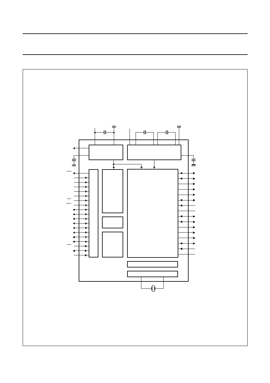
GENERAL DESCRIPTION
The TDA8007B is a low cost card interface for dual smart
card readers. Controlled through a parallel bus, it takes
care of all ISO 7816, EMV and GSM11-11 requirements.
It may be interfaced to the P0/P2 ports of a 80C51 family
microcontroller, and be addressed as a memory through
MOVX instructions. It may also be addressed on a
non-multiplexed 8-bit data bus, by means of address
registers AD0, AD1, AD2 and AD3. The integrated ISO
UART and the time-out counters allow easy use even at
high baud rates with no real time constraints. Due to its
chip select and external I/O and INT features, it greatly
simplifies the realization of any number of cards readers.
It gives the cards and the reader a very high level of
security, due to its special hardware against ESD,
short-circuiting, power failure, etc. Its integrated step-up
converter allows operation within a supply voltage range of
2.7 to 6 V.
A software library has been developed, taking care of all
actions required for T = 0, T = 1 and synchronous
protocols (see application reports).
ORDERING INFORMATION
TYPE
NUMBER
PACKAGE
NAME
DESCRIPTION
VERSION
TDA8007BHL
LQFP48
plastic low profile quad flat package; 48 leads; body 7
◊
7
◊
1.4 mm
SOT313-2
2000 Nov 09
3
Philips Semiconductors
Product specification
Double multiprotocol IC card interface
TDA8007B
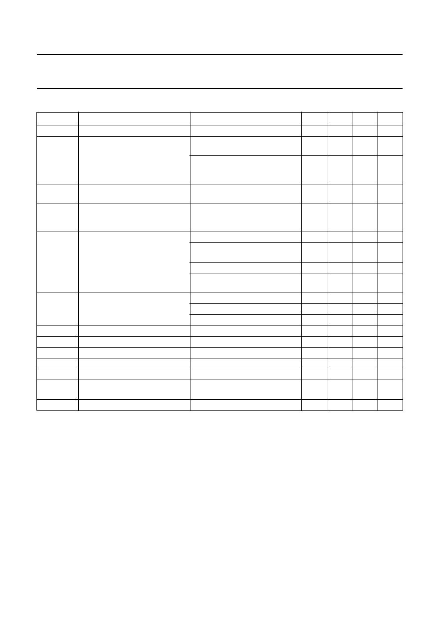
QUICK REFERENCE DATA
SYMBOL
PARAMETER
CONDITIONS
MIN.
TYP.
MAX.
UNIT
V
DD
supply voltage
2.7
-
6
V
I
DD(pd)
supply current in power-down
mode
V
DD
= 3.3 V; cards inactive; XTAL
oscillator stopped
-
-
350
µ
A
V
DD
= 3.3 V; cards active at
V
CC
= 5 V; CLK stopped; XTAL
oscillator stopped
-
-
3
mA
I
DD(sm)
supply current in sleep mode
cards powered at 5 V but clock
stopped
-
-
5.5
mA
I
DD(om)
supply current in operating mode
V
DD
= 3.3 V; f
XTAL
= 20 MHz;
V
CC1
= V
CC2
= 5 V;
I
CC1
+ I
CC2
= 80 mA
-
-
315
mA
V
CC
output card supply voltage
including static loads (5 V card)
4.75
5.0
5.25
V
with 40 nC dynamic loads on
200 nF capacitor (5 V card)
4.6
-
5.4
V
including static loads (3 V card)
2.78
-
3.22
V
with 24 nC dynamic loads on
200 nF capacitor (3 V card)
2.75
-
3.25
V
I
CC
output card supply current
operating; 5 V card
-
-
65
mA
operating; 3 V card
-
-
50
mA
overload detection
-
100
-
mA
I
CC1
+ I
CC2
sum of both cards currents
-
-
80
mA
SR
slew rate on V
CC
(rise and fall)
C
L(max)
= 300 nF
0.05
0.16
0.22
V/
µ
s
t
deact
deactivation cycle duration
-
-
150
µ
s
t
act
activation cycle duration
-
-
225
µ
s
f
xtal
crystal frequency
4
-
27
MHz
f
op
operating frequency
external frequency applied to pin
XTAL1
0
-
25
MHz
T
amb
ambient temperature
-
25
-
+85
∞
C

2000 Nov 09
5
Philips Semiconductors
Product specification
Double multiprotocol IC card interface
TDA8007B
PINNING
SYMBOL
PIN
DESCRIPTION
RSTOUT
1
open-drain output for resetting external chips
I/OAUX
2
input or output for an I/O line issued of an auxiliary smart card interface
I/O1
3
data line to/from card 1 (ISO C7 contact)
C81
4
auxiliary I/O for ISO C8 contact (synchronous cards for instance) for card 1
PRES1
5
card 1 presence contact input (active HIGH or LOW by mask option)
C41
6
auxiliary I/O for ISO C4 contact (synchronous cards for instance) for card 1
GNDC1
7
ground for card 1
CLK1
8
clock output to card 1 (ISO C3 contact)
V
CC1
9
card 1 supply output voltage (ISO C1 contact)
RST1
10
card 1 reset output (ISO C2 contact)
I/O2
11
data line to/from card 2 (ISO C7 contact)
C82
12
auxiliary I/O for ISO C8 contact (synchronous cards for instance) for card 2
PRES2
13
card 2 presence contact input (active HIGH or LOW by mask option)
C42
14
auxiliary I/O for ISO C4 contact (synchronous cards for instance) for card 2
GNDC2
15
ground for card 2
CLK2
16
clock output to card 2 (ISO C3 contact)
V
CC2
17
card 2 supply output voltage (ISO C1 contact)
RST2
18
card 2 reset output (ISO C2 contact)
GND
19
ground connection
V
UP
20
output of the step-up converter
SAP
21
contact 1 for the step-up converter (connect a low ESR 220 nF capacitor between pins SAP
and SAM)
SBP
22
contact 3 for the step-up converter (connect a low ESR 220 nF capacitor between pins SBP
and SBM)
V
DDA
23
positive analog supply voltage for the step-up converter
SBM
24
contact 4 for the step-up converter (connect a low ESR 220 nF capacitor between pins SBP
and SBM)
AGND
25
ground connection for the step-up converter
SAM
26
contact 2 for the step-up converter (connect a low ESR 220 nF capacitor between pins SAP
and SAM)
V
DD
27
positive supply voltage
D0
28
data 0 or add 0
D1
29
data 1 or add 1
D2
30
data 2 or add 2
D3
31
data 3 or add 3
D4
32
data 4 or add 4
D5
33
data 5 or add 5
D6
34
data 6 or add 6
D7
35
data 7 or add 7
RD
36
read selection signal (read or write in non-multiplexed configuration)