 | –≠–ª–µ–∫—Ç—Ä–æ–Ω–Ω—ã–π –∫–æ–º–ø–æ–Ω–µ–Ω—Ç: TDA8260 | –°–∫–∞—á–∞—Ç—å:  PDF PDF  ZIP ZIP |

DATA SHEET
Product specification
Supersedes data of 2003 Jun 11
2004 Sep 03
INTEGRATED CIRCUITS
TDA8260TW
Satellite Zero-IF QPSK/8PSK
downconverter with PLL
synthesizer

2004 Sep 03
2
Philips Semiconductors
Product specification
Satellite Zero-IF QPSK/8PSK
downconverter with PLL synthesizer
TDA8260TW
FEATURES
∑
Direct conversion Quadrature Phase Shift
Keying (QPSK) and 8-Phase Shift Keying (8PSK)
demodulation (Zero-IF)
∑
Frequency range: 950 to 2175 MHz
∑
High level asymmetrical RF input
∑
0 to 50 dB variable gain with AGC control
∑
Loop-controlled 0 to 90
∞
phase shifter
∑
High AGC linearity (<1 dB per bit with an 8-bit DAC),
AGC voltage variable between 0 and 3 V
∑
Integrated 5th-order matched baseband filters for
in-phase (I) and quadrature (Q) signal paths
∑
Controlled I-to-Q gain balance
∑
I
2
C-bus controlled PLL frequency synthesizer
∑
Low phase noise
∑
Operation from a 4 MHz crystal (allowing the use of
an SMD crystal)
∑
Five frequency steps from 125 kHz to 2 MHz
∑
Crystal frequency output to drive the demodulator IC
∑
Compatible with 5, 3.3 and 2.5 V I
2
C-bus
∑
Fully compatible and easy to interface with Philips
Semiconductors family of digital satellite demodulators
∑
+5 V DC supply voltage
∑
38-pin high heat dissipation package.
APPLICATIONS
∑
Direct Broadcasting Satellite (DBS) QPSK
demodulation
∑
Digital Video Broadcasting (DVB) QPSK demodulation
∑
BS digital 8PSK demodulation.
GENERAL DESCRIPTION
The direct conversion QPSK demodulator is the front-end
receiver dedicated to digital TV broadcasting, satisfying
both DVB and DBS TV standards. The wide range
oscillator (from 950 to 2175 MHz) covers the American,
European and Asian satellite bands, as well as the
SMA-TV US standard.
The Zero-IF concept discards traditional IF filtering and
intermediate conversion techniques. It also simplifies the
signal path.
Optimum signal level is guaranteed by gain-controlled
amplifiers in the RF path. The 0 to 50 dB variable gain is
controlled by the signal returned from the Satellite
Demodulator and Decoder (SDD) and applied to
pin AGCIN.
The PLL synthesizer is built on a dual-loop concept. The
first loop controls a fully integrated L-band oscillator, using
as a reference the LC VCO which runs at a quarter of the
synthesized frequency.
The second loop controls the tuning voltage of the VCO
and improves the phase noise of the carrier within the loop
bandwidth. The step size is equal to the comparison
frequency. The input of the main divider of the PLL
synthesizer is connected internally to the VCO output.
The comparison frequency of the second loop is obtained
from an oscillator driven by an external 4 MHz crystal. The
4 MHz output available at pin XTOUT may be used to drive
the crystal inputs of the SDD, thereby saving an additional
crystal in the application.
Both the divided and the comparison frequencies of the
second loop are compared in a fast phase detector which
drives the charge pump. The TDA8260TW includes a loop
amplifier with an internal high-voltage transistor to drive an
external 33 V tuning voltage.
Control data is entered via the I
2
C-bus. The I
2
C-bus
voltage can be 5.0, 3.3 or 2.5 V, thus allowing
compatibility with most existing microcontrollers.
A 5-byte frame is required to address the device and to
program the main divider ratio, the reference divider ratio,
the charge pump current and the operating mode.
A flag is set when the loop is `in-lock', this can be read
during READ operations, as well as the Power-on reset
flag.
The device has four selectable I
2
C-bus addresses. The
selection is done by applying a specific voltage to pin AS.
This feature gives the possibility to use up to four
TDA8260TW ICs in the same system.

2004 Sep 03
3
Philips Semiconductors
Product specification
Satellite Zero-IF QPSK/8PSK
downconverter with PLL synthesizer
TDA8260TW
Performance summary
TDA8260TW performance:
∑
Noise figure at maximum gain = +18 dB
∑
High linearity; IP2 = +19 dBm and IP3 = +14 dBm
∑
Low phase noise on baseband outputs:
-
78 dBc/Hz (f
offset
= 1 and 10 kHz; f
COMP
= 1 MHz)
∑
0 to 50 dB variable gain with AGC control
∑
AGC linearity <1 dB/bit with an 8-bit DAC
∑
Maximum I-to-Q amplitude mismatch = 1 dB
∑
Maximum I-to-Q phase mismatch = 3
∞
∑
Signal rates from 1 to 45 MSymbol/s.
System performance, for example, in a tuner application
with the IC placed after a low-cost discrete LNA
(see Fig.11):
∑
Noise figure at maximum gain = 8 dB
∑
High linearity; IP2 = +15 dBm and IP3 = +5 dBm
∑
0 to 50 dB variable gain with AGC control.
Specification limitation
The content of this specification is applies to the device
TDA8260TW with versions C2 and above. Version C1 is
not covered by this document. Please contact your Philips
semiconductors representative for further information.
QUICK REFERENCE DATA
ORDERING INFORMATION
SYMBOL
PARAMETER
CONDITIONS
MIN.
TYP.
MAX.
UNIT
V
CC
supply voltage
4.75
5.0
5.25
V
I
CC
supply current
-
155
-
mA
f
osc
oscillator frequency
950
-
2175
MHz
Eq
quadrature error (absolute value)
V
AGC
= 1.5 V;
V
o(p-p)
= 750 mV;
measured in baseband
-
0
3
deg
V
o(p-p)
recommended output voltage
(peak-to-peak value)
-
750
-
mV
LPF
CO
LPF cut-off frequency
-
36
-
MHz
n
phase noise on baseband outputs f
offset
= 1 and 10 kHz;
f
COMP
= 1 MHz with
appropriate loop filter and
charge pump setting
-
-
-
78
dBc/Hz
G
v
AGC range
V
AGC
= 0 to 3 V
48
50
-
dB
V
XTOUT(p-p)
AC output voltage on pin XTOUT
(peak-to-peak value)
T
2
= 1, T
1
= 0, T
0
= 0;
driving a load of
C
L
= 10 pF, R
L
= 1 M
500
650
-
mV
T
amb
ambient temperature
-
20
-
+85
∞
C
TYPE
NUMBER
PACKAGE
NAME
DESCRIPTION
VERSION
TDA8260TW
HTSSOP38 plastic thermal enhanced thin shrink small outline package; 38 leads;
body width 6.1 mm; lead pitch 0.65 mm; exposed die pad
SOT633-3

2004 Sep 03
4
Philips Semiconductors
Product specification
Satellite Zero-IF QPSK/8PSK
downconverter with PLL synthesizer
TDA8260TW
BLOCK DIAGRAM
handbook, full pagewidth
25
13
12
17
26
6
27
15
24
11
10
7
8
31
28
3
4
9
AGC
CONTROL
VCO
fDIV
fXTAL
fCOMP
FAST PHASE/
FREQUENCY
COMPARATOR
DIGITAL PHASE
COMPARATOR
REFERENCE
DIVIDER
POWER-ON
RESET
CONTROL LOGIC
AND LATCH
OSCILLATOR
CHARGE PUMP
DIVIDE-BY-4
15-BIT DIVIDER
33 V
AMP
14
16
23
21
22
20
19
18
38
33
34
5
I
Q
integrated
oscillator
29
30
2
1
I
2
C-BUS
36
37
32
35
TDA8260TW
MGU790
XTOUT
SDA
SCL
AS
CP
VT
BVS
VCC(VCO)
TKA
TKB
VCOGND
CAP1 CAP2
IOUT
BBGND2
IBBIN
n.c.
IBBOUT
IIN
XT1
XT2
VCC(PLL)
PLLGND
AGCIN
BIASN
RFGND1
VCC(RF)
RFA
RFB
RFGND2
LP1 LP2
QOUT
BBGND1
QBBIN
VCC(BB)
QBBOUT
QIN
Fig.1 Block diagram.

2004 Sep 03
5
Philips Semiconductors
Product specification
Satellite Zero-IF QPSK/8PSK
downconverter with PLL synthesizer
TDA8260TW
PINNING INFORMATION
SYMBOL
PIN
DESCRIPTION
XT1
1
4 MHz crystal oscillator input 1
XT2
2
4 MHz crystal oscillator input 2
V
CC(PLL)
3
supply voltage for PLL circuit (+5 V)
PLLGND
4
ground for PLL circuit
AGCIN
5
AGC input from satellite demodulator and decoder
BIASN
6
RF isolation input (+5 V)
RFGND1
7
ground 1 for RF circuit
V
CC(RF)
8
supply voltage for RF stage (+5 V)
RFA
9
RF signal input A
RFB
10
RF signal input B
RFGND2
11
ground 2 for RF circuit
LP1
12
low-pass filter loop filtering output
LP2
13
low-pass filter loop filtering input
QOUT
14
quadrature output for AC coupling to pin 16
BBGND1
15
ground 1 for baseband stage
QBBIN
16
quadrature baseband AC-coupled input from pin 14
V
CC(BB)
17
supply voltage for baseband stage (+5 V)
QBBOUT
18
quadrature baseband output to satellite demodulator and decoder
QIN
19
quadrature input for auto-amplitude matching
IIN
20
in-phase input for auto-amplitude matching
IBBOUT
21
in-phase baseband output to satellite demodulator and decoder
n.c.
22
not connected
IBBIN
23
in-phase AC-coupled baseband input from pin 25
BBGND2
24
ground 2 for baseband stage
IOUT
25
in-phase output for AC-coupling to pin 23
CAP2
26
amplitude matching loop filtering output 2
CAP1
27
amplitude matching loop filtering output 1
VCOGND
28
ground for VCO circuit
TKB
29
VCO tank circuit input B
TKA
30
VCO tank circuit input A
V
CC(VCO)
31
supply voltage for VCO circuit (+5 V)
BVS
32
bus voltage select input
VT
33
tuning voltage output for VCO
CP
34
charge pump output
AS
35
address selection input
SCL
36
I
2
C-bus clock input
SDA
37
I
2
C-bus data input/output
XTOUT
38
4 MHz crystal oscillator output to satellite demodulator and decoder
2004 Sep 03
6
Philips Semiconductors
Product specification
Satellite Zero-IF QPSK/8PSK
downconverter with PLL synthesizer
TDA8260TW
FUNCTIONAL DESCRIPTION
The TDA8260TW contains the core of the RF analog part
of a digital satellite receiver. The signal coming from the
Low Noise Block (LNB) is coupled through a Low Noise
Amplifier (LNA) to the RF inputs. The internal circuitry
performs the Zero-IF quadrature frequency conversion
and the two in-phase (IBBOUT) and quadrature
(QBBOUT) output signals can be used directly to feed a
Satellite Demodulator and Decoder circuit (SDD).
The TDA8260TW has a gain-controlled amplifier in the
converter circuit. The gain is controlled by the AGCIN input
from the SDD.
An external VCO tank circuit is connected between pins
TKA and TKB. The main elements of the external tank
circuit are an SMD coil and a varactor diode. The tuning
voltage of 0 to 30 V covers the whole frequency range
from 237.5 to 543.75 MHz. The internal loop controls a
fully integrated VCO to cover the range 950 to 2175 MHz.
The VCO provides both in-phase and quadrature signals
to drive the two mixers.
Except for the 4 MHz crystal and the loop filter, all circuit
components necessary to control the varactor-tuned
oscillator are integrated in the TDA8260TW. The tuning
circuit includes a fast phase detector with a high
comparison frequency in order to achieve the lowest
possible level of phase noise in the local oscillator.
The f
DIV
output of the15-bit programmable divider passes
through the fast phase comparator where it is compared in
both phase and frequency with the comparison frequency
(f
COMP
). The frequency f
COMP
is derived from the signal
present at the XT1/XT2 pins (f
XTAL
) divided-down by the
reference divider. The buffered XTOUT signal can drive
the crystal frequency input of the SDD, thereby saving a
crystal in the application.
The output of the phase comparator drives the charge
pump and loop amplifier section. The loop amplifier
includes a high voltage transistor to handle the 30 V tuning
voltage at pin VT, this drives a variable capacitance diode
in the external circuit of the voltage controlled oscillator.
Pin CP is the output of the charge pump. The loop filter is
connected between pins CP and VT and the post-filter
section is connected between pin VT and the variable
capacitance diode.
For test and alignment purposes, it is possible to release
the tuning voltage output and apply an external voltage to
pin VT, also to select the charge pump function to sink
current, source current or to be switched off.
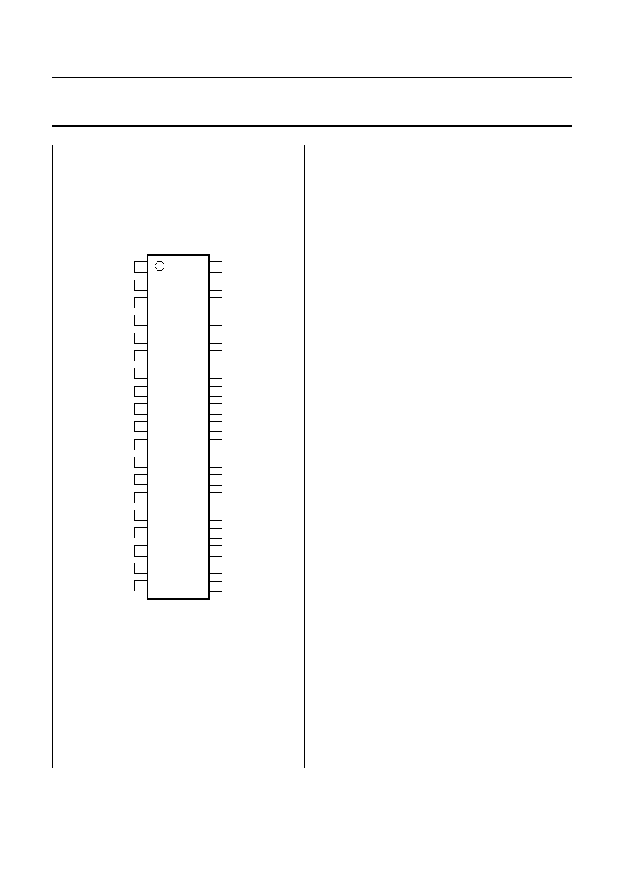
handbook, halfpage
TDA8260TW
MGU791
1
2
3
4
5
6
7
8
9
10
11
12
13
14
15
16
17
18
19
38
37
36
35
34
33
32
31
30
29
28
27
26
25
24
23
22
21
20
XTOUT
SDA
SCL
AS
CP
VT
BVS
VCC(VCO)
TKA
TKB
VCOGND
CAP1
CAP2
IOUT
BBGND2
IBBIN
n.c.
IBBOUT
IIN
XT1
XT2
VCC(PLL)
PLLGND
AGCIN
BIASN
RFGND1
VCC(RF)
RFA
RFB
RFGND2
LP1
LP2
QOUT
BBGND1
QBBIN
VCC(BB)
QBBOUT
QIN
Fig.2 Pin configuration.
2004 Sep 03
7
Philips Semiconductors
Product specification
Satellite Zero-IF QPSK/8PSK
downconverter with PLL synthesizer
TDA8260TW
PROGRAMMING
The programming of the TDA8260TW is performed
through the I
2
C-bus. The read/write selection is made
through the R/W bit (address LSB). The TDA8260TW
fulfils the I
2
C-bus fast mode, according to the Philips
I
2
C-bus specification, see document
"9398 393 40011".
I
2
C-bus voltage
The I
2
C-bus lines SCL and SDA can be connected to an
I
2
C-bus system tied either to 2.5, 3.3 or 5.0 V, that will
allow direct connection to most existing microcontrollers.
The choice of the threshold voltage for the I
2
C-bus lines is
made with pin BVS that needs to be left open-circuit,
connected to supply voltage or connected to ground;
see Table 1.
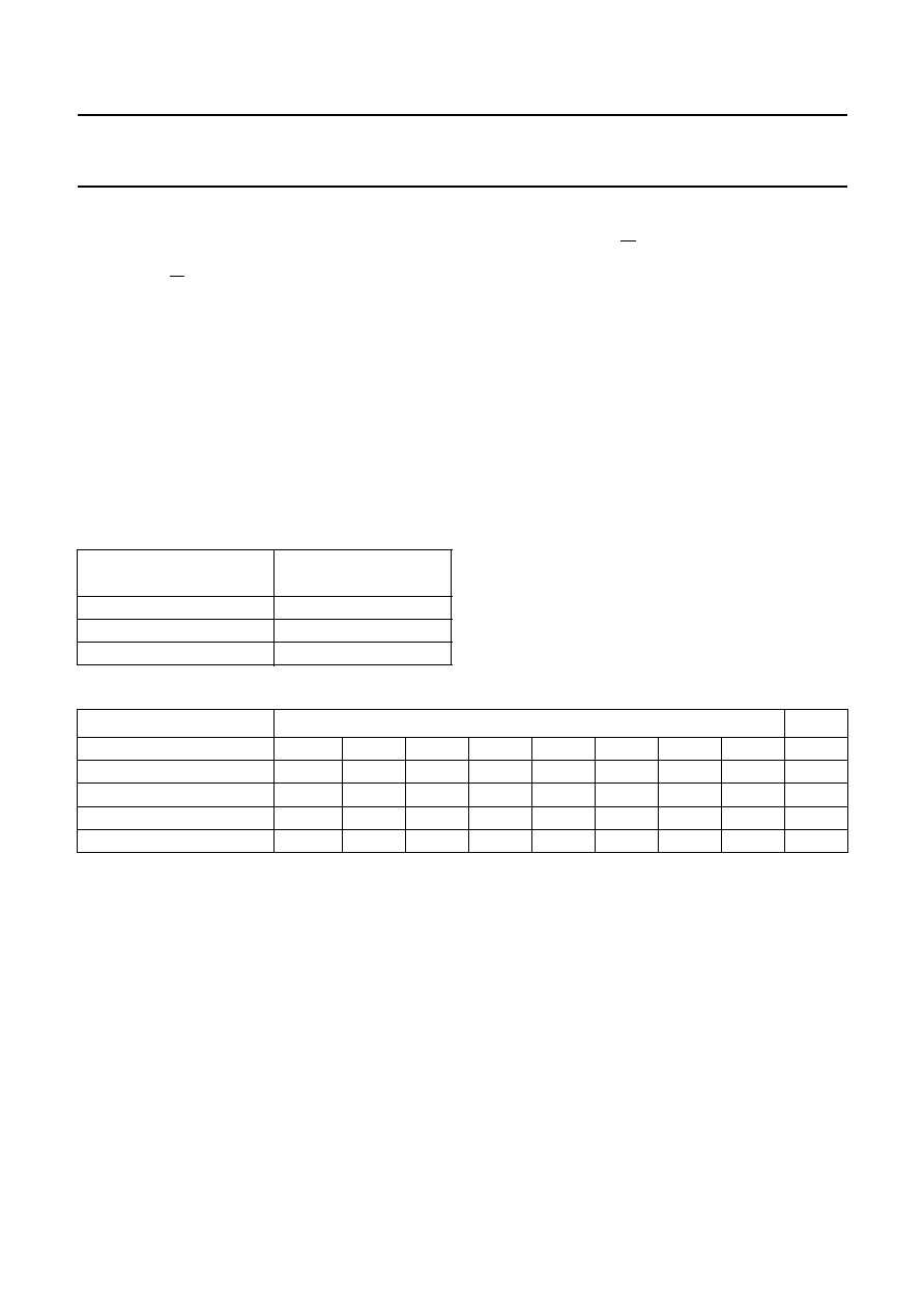
Table 1
I
2
C-bus voltage selection
I
2
C-bus write mode
I
2
C-bus write mode: R/W = logic 0; see Table 2.
After transmission of the address (first byte), four data
bytes can be sent to fully program the TDA8260TW. The
transmission sequence is one address byte followed by
four data bytes PD1, PD2, CD1 and CD2.
The I
2
C-bus transceiver has an auto-increment facility that
permits the TDA8260TW to be programmed within a
single transmission.
The TDA8260TW can be partly programmed provided that
the first data byte following the address is PD1 or CD1.
The first bit of the first data byte transmitted indicates
whether PD1 (first bit = logic 0) or CD1 (first bit = logic 1)
will follow.
Additional data bytes can be entered without the need to
re-address the device until an I
2
C-bus STOP condition is
sent by the controller. Each byte is loaded after the
corresponding 8th clock pulse.
Programmable divider data (contents of PD1 and PD2)
become valid only after the 8th clock pulse of PD2, or after
a STOP condition if only PD1 needs to be programmed.
PIN BVS
I
2
C-BUS VOLTAGE
(V)
GND
2.5
Open-circuit
3.3
V
CC
5
Table 2
I
2
C-bus write data format
Notes
1. MSB is transmitted first.
2. X = undefined.
3. Acknowledge bit (A).
BYTE
(MSB)
(1)
BITS
(2)
(LSB)
ACK
(3)
Programmable address
1
1
0
0
0
MA1
MA0
0
A
Programmable divider (PD1)
0
N14
N13
N12
N11
N10
N9
N8
A
Programmable divider (PD2)
N7
N6
N5
N4
N3
N2
N1
N0
A
Control data (CD1)
1
T2
T1
T0
R2
R1
R0
X
A
Control data (CD2)
C1
C0
X
X
X
X
X
X
A

2004 Sep 03
8
Philips Semiconductors
Product specification
Satellite Zero-IF QPSK/8PSK
downconverter with PLL synthesizer
TDA8260TW
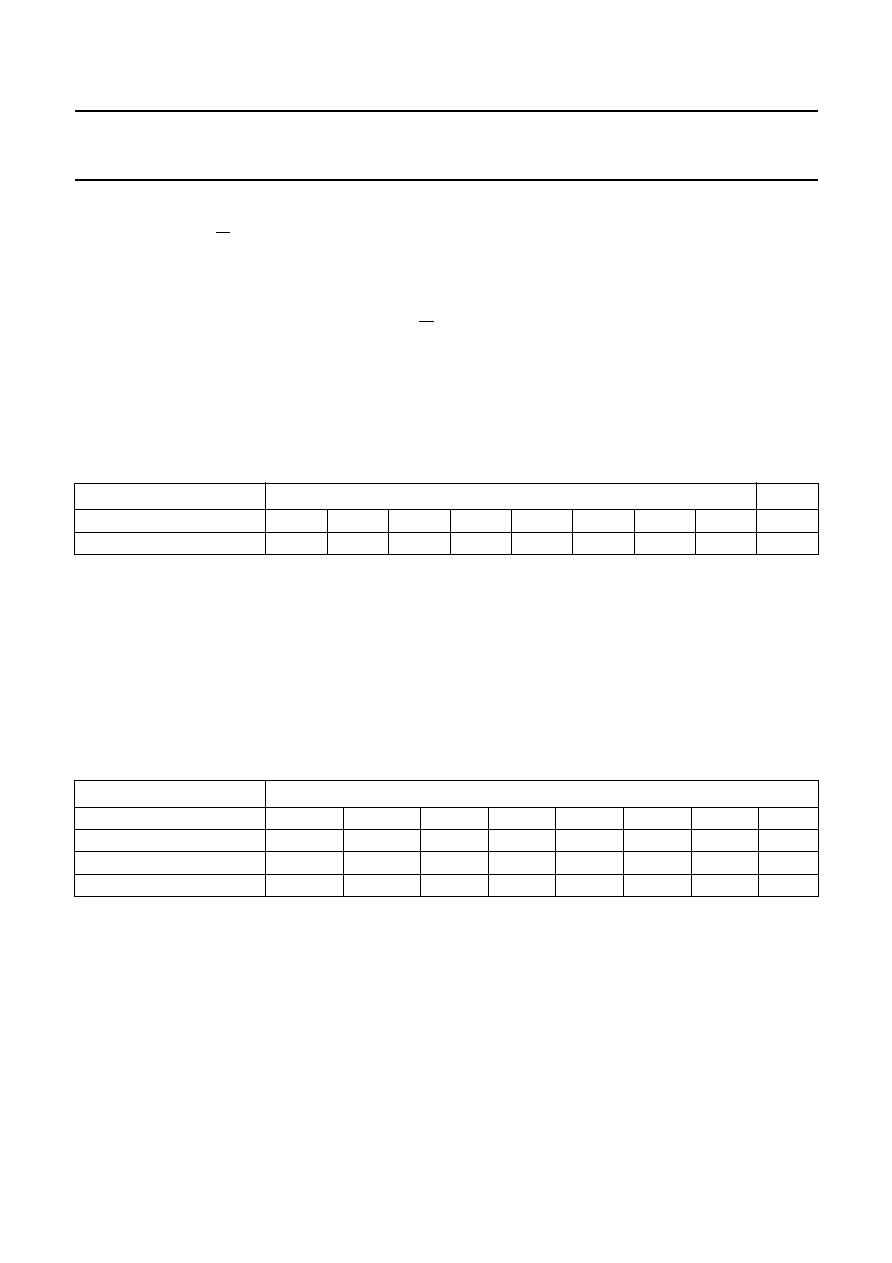
P
ROGRAMMABLE ADDRESSES
The programmable address bits MA1 and MA0 offer the
possibility of having up to four TDA8260TW devices in the
same system. The relationship between the voltage
applied to pin AS and the value of bits MA1 and MA0 is
given in Table 3.
Table 3
I
2
C-bus address selection
P
ROGRAMMABLE MAIN DIVIDER RATIO
Program bytes PD1 and PD2 contain the fifteen bits
N14 to N0 that set the main divider ratio. The ratio
N = N14
◊
2
14
+ N13
◊
2
13
+...+ N1
◊
2 + N0.
O
PERATING AND TEST MODES
The mode of operation is set using bits T2, T1 and T0 in
control byte CD1; see Table 4.
Table 4
Mode selection
Note
1. Status at power-on: the tuning voltage output is
released and pin VT is in the high-impedance state.
R
EFERENCE DIVIDER
Five reference divider ratios allow the adjustment of the
comparison frequency to different values depending on
the compromise that has to be found between step size
and phase noise. The reference divider ratios and the
corresponding comparison frequencies are programmed
using bits R2, R1 and R0; see Table 5.
Table 5
Reference divider ratio
C
HARGE PUMP CURRENT
Four values of charge pump current can be chosen using
bits C1 and C0; see Table 6.
Table 6
Charge pump current
V
AS
MA1
MA0
0 to 0.1V
CC
0
0
open-circuit
0
1
0.4V
CC
to 0.6V
CC
1
0
0.9V
CC
to V
CC
1
1
T2
T1
T0
MODE
XTOUT
0
0
0
normal operation
OFF
0
0
1
POR state = CP sink
(1)
f
XTAL
0
1
0
1
/
2
◊
f
DIV
1
/
2
◊
f
DIV
0
1
1
CP sink
f
XTAL
1
0
0
normal operation
f
XTAL
1
0
1
2
◊
f
ref
2
◊
f
ref
1
1
0
CP OFF
f
XTAL
1
1
1
CP source
f
XTAL
R2
R1
R0
DIVIDER RATIO
COMPARISON
FREQUENCY
0
0
0
2
2 MHz
0
0
1
4
1 MHz
0
1
0
8
500 kHz
0
1
1
not allowed
1
0
0
not allowed
1
0
1
16
250 kHz
1
1
0
not allowed
1
1
1
32
125 kHz
C1
C0
TYPICAL CHARGE PUMP
CURRENT ABSOLUTE VALUES
(
µ
A)
0
0
420
0
1
900
1
0
1360
1
1
2320
2004 Sep 03
9
Philips Semiconductors
Product specification
Satellite Zero-IF QPSK/8PSK
downconverter with PLL synthesizer
TDA8260TW
I
2
C-bus read mode
I
2
C-bus read mode: R/W = logic 1 (address LSB;
see Table 7).
When a read sequence is started, all eight bits of the status
byte must be read.
Data can be read from the TDA8260TW by setting the R/W
bit to logic 1. After recognition of its slave address, the
TDA8260TW generates an acknowledge pulse and
transfers the status byte onto the SDA line (MSB first).
Data is valid on the SDA line when the SCL clock signal is
HIGH.
A second data byte can be read from the TDA8260TW if
the microcontroller generates an acknowledge on the SDA
line. End of transmission will occur if no acknowledge is
received from the microcontroller. The TDA8260TW will
then release the data line to allow the microcontroller to
generate a STOP condition.
The POR flag (Power-on reset) is set to logic 1 at
power-on and when V
CC
goes below 2.7 V. It is reset to
logic 0 when an end-of-data condition is detected by the
TDA8260TW (end of a READ sequence).
The in-lock flag FL indicates that the loop is phase-locked
when set to logic 1.
Table 7
I
2
C-bus read data format
Notes
1. Acknowledge bit (A).
2. FL is valid only in normal mode.
3. X can be 1 or 0 and needs to be masked in the microcontrollers' software; MSB is transmitted first.
P
OWER
-
ON RESET
Power-on reset flag POR = 1 at power-on.
At power-on, or when the supply voltage drops below 2.7 V, internal registers are reset as shown in Table 8.
Table 8
Status at Power-on reset
Note
1. X = not set.
BYTE
(MSB)
BITS
(LSB)
ACK
(1)
Address
1
1
0
0
0
MA1
MA0
1
A
Status byte
POR
FL
(2)
X
(3)
X
(3)
X
(3)
X
(3)
X
(3)
X
(3)
-
BYTE
(MSB)
BITS
(1)
(LSB)
Programmable divider (PD1)
0
N14 = X
N13 = X
N12 = X
N11 = X
N10 = X
N9 = X
N8 = X
Programmable divider (PD2)
N7 = X
N6 = X
N5 = X
N4 = X
N3 = X
N12 = X
N1 = X
N0 = X
Control data (CD1)
1
T2 = 0
T1 = 0
T0 = 1
R2 = X
R1 = X
R0 = X
X
Control data (CD2)
C1 = X
C0 = X
X
X
X
X
X
X

2004 Sep 03
10
Philips Semiconductors
Product specification
Satellite Zero-IF QPSK/8PSK
downconverter with PLL synthesizer
TDA8260TW
LIMITING VALUES
In accordance with the Absolute Maximum Rating System (IEC 60134); see note 1.
Note
1. Maximum ratings cannot be exceeded, not even momentarily, without causing irreversible damage to the IC.
Maximum ratings cannot be accumulated.
THERMAL CHARACTERISTICS
HANDLING
Inputs and outputs are protected against electrostatic discharge in normal handling. However it is good practice to take
normal precautions appropriate to handling MOS devices (see
"Handling MOS devices").
ESD specification:
∑
Every pin withstands 2000 V in the ESD test in accordance with
JEDEC specification EIA/JESD-A114A, HBM model
(category 2); except pins SCL (pin 36), VT (pin 33) and V
CC(RF)
(pin 8).
∑
Identically every pin withstands 200 V in the ESD test in accordance with
JEDEC specification EIA/JESD22-A115A,
MM model (category B); except pins TKA (pin 30) and TKB (pin 29).
SYMBOL
PARAMETER
MIN.
MAX.
UNIT
V
CC
supply voltage
-
0.3
+6.0
V
V
i(max)
; V
o(max)
maximum input or output voltage on all pins except SDA, SCL and VT
-
0.3
V
CC
+ 0.3
V
V
i(SDA)
; V
o(SDA)
data input or data output voltage
-
0.3
+6.0
V
V
i(SCL)
clock input voltage
-
0.3
+6.0
V
V
o(tune)
tuning voltage output
-
0.3
+35
V
T
amb
ambient temperature
-
20
+85
∞
C
T
stg
IC storage temperature
-
40
+150
∞
C
T
j(max)
maximum junction temperature
-
150
∞
C
t
sc(max)
maximum short-circuit time; each pin; short-circuit to V
CC
or GND
-
10
s
SYMBOL
PARAMETER
CONDITIONS
VALUE
UNIT
R
th(j-a)
thermal resistance from junction to ambient
in free air
39
K/W

2004 Sep 03
11
Philips Semiconductors
Product specification
Satellite Zero-IF QPSK/8PSK
downconverter with PLL synthesizer
TDA8260TW
CHARACTERISTICS
T
amb
= 25
∞
C; V
CC
= 5 V; R
L
= 1 k
and V
o(p-p)
= 750 mV on baseband output pins IBBOUT and QBBOUT; unless
otherwise specified.
SYMBOL
PARAMETER
CONDITIONS
MIN.
TYP.
MAX.
UNIT
Supply
V
CC
supply voltage
4.75
5.00
5.25
V
I
CC
supply current
-
155
-
mA
V
CC(POR)
supply voltage threshold for
POR active
-
2.7
-
V
Performance from RF inputs to I, Q outputs (from pins RFA, RFB to pins IBBOUT, QBBOUT)
P
L(LO)
LO power leakage through
pins RFA and RFB
-
-
75
-
dBm
G
v(RF-BBOUT)(max)
maximum voltage gain from pins
RFA, RFB to IBBOUT, QBBOUT
V
AGC
= 3 V
55
57
-
dB
G
v
AGC range
V
AGC
= 0 to 3 V
48
50
-
dB
V
o(p-p)
output voltage (peak-to-peak
value)
recommended value
-
750
-
mV
IP2i
2nd-order interception point
at RF input; V
AGC
= 0 V
-
19
-
dBm
IP3i
3rd-order interception point
at RF input; V
AGC
= 0 V
-
14
-
dBm
F
noise figure
at maximum gain;
V
AGC
= 3 V
-
18
-
dB
G
v(IQ)
voltage gain mismatch between
I and Q
in 22.5 MHz band
-
-
1
dB
Eq
quadrature error (absolute
value)
V
AGC
= 1.5 V;
V
o(p-p)
= 750 mV;
measured in baseband
-
0
3
deg
G
v(IQ)ripple
voltage gain ripple for I or Q
in 30 MHz band
-
-
2
dB
t
d(g)(IQ)(R)
group delay ripple for I or Q
in 22.5 MHz band
-
5
-
ns
RR
60
ripple rejection for I and Q
f
ripple
= 60 MHz
30
-
-
dB
Pulling sensitivity
3/4LO
sensitivity to pulling on the third
harmonic of the external VCO
see Table 9
-
-
40
-
35
dBc
5/4LO
sensitivity to pulling on the fifth
harmonic of the external VCO
see Table 9
-
-
40
-
35
dBc
VCO and synthesizer
f
osc
oscillator frequency range
950
-
2175
MHz
n(osc)
oscillator phase noise
in the satellite band;
f
offset
= 100 kHz; out of
PLL loop bandwidth
-
-
100
-
94
dBc/Hz
n
phase noise on baseband
outputs
f
offset
= 1 and 10 kHz;
f
COMP
= 1 MHz with
appropriate loop filter
and charge pump
setting
-
-
-
78
dBc/Hz

2004 Sep 03
12
Philips Semiconductors
Product specification
Satellite Zero-IF QPSK/8PSK
downconverter with PLL synthesizer
TDA8260TW
MDR
main divider ratio
64
-
32767
Z
osc
crystal oscillator negative
impedance (absolute value)
1.0
1.5
-
k
f
XTAL
crystal frequency
-
4
-
MHz
V
XTOUT(p-p)
AC output voltage on
pin XTOUT (peak-to-peak value)
T
2
= 1, T
1
= 0, T
0
= 0;
driving a load of
C
L
= 10 pF, R
L
= 1 M
500
650
-
mV
Z
XTAL
crystal series impedance
recommended value
-
-
200
Charge pump output; pin CP
I
L(CP)
charge pump leakage current
T
2
= 1; T
1
= 1; T
0
= 0
-
10
0
+10
nA
Tuning voltage output; pin VT
I
LO(off)
leakage current when pin VT is
in high-impedance off-state
T
2
= 0; T
1
= 0; T
0
= 1;
V
tune
= 33 V
-
-
10
µ
A
V
o
output voltage when the loop is
locked
normal mode;
V
tune
= 33 V
0.2
-
32.7
V
Bus voltage select input; pin BVS
I
LIH
HIGH-level input leakage
current
V
BVS
= V
CC
-
-
100
µ
A
I
LIL
LOW-level input leakage current
V
BVS
= 0 V
-
100
-
-
µ
A
SCL and SDA inputs
V
IL
LOW-level input voltage
pin BVS floating
-
-
0.2V
CC
V
V
BVS
= 0 V
-
-
0.15V
CC
V
V
BVS
= 5 V
-
-
0.3V
CC
V
V
IH
HIGH-level input voltage
pin BVS floating
0.46V
CC
-
-
V
V
BVS
= 0 V
0.35V
CC
-
-
V
V
BVS
= 5 V
0.6V
CC
-
-
V
I
LIH
HIGH-level leakage current
V
IH
= 5.5 V;
V
CC
= 5.5 V
-
-
10
µ
A
V
IH
= 5.5 V; V
CC
= 0 V
-
-
10
µ
A
I
LIL
LOW-level leakage current
V
IL
= 0 V; V
CC
= 5.5 V
-
10
-
-
µ
A
f
SCL(max)
maximum input clock frequency
400
-
-
kHz
SDA output
V
ACK
output voltage during
acknowledge
I
sink
= 3 mA
-
-
0.4
V
AS input
I
IH
HIGH-level input current
V
AS
= V
CC
-
-
10
µ
A
I
IL
LOW-level input current
V
AS
= 0 V
-
10
-
-
µ
A
SYMBOL
PARAMETER
CONDITIONS
MIN.
TYP.
MAX.
UNIT

2004 Sep 03
13
Philips Semiconductors
Product specification
Satellite Zero-IF QPSK/8PSK
downconverter with PLL synthesizer
TDA8260TW
handbook, halfpage
f (MHz)
G
(dB)
950
1350
1750
2150
1150
1550
1950
68
64
56
52
60
MGU797
Fig.3
Overall maximum gain as a function of
frequency.
handbook, halfpage
VAGC (V)
G
(dB)
0
1
2
3
80
60
20
0
40
MGU799
Fig.4 Overall gain as a function of AGC voltage.
handbook, halfpage
F
(dB)
MGU798
f (MHz)
950
1350
1750
2150
1150
1550
1950
20
16
18
14
12
10
Fig.5
Noise figure at maximum gain as a function
of frequency.
handbook, halfpage
n
(dBc/Hz)
-
70
-
80
-
100
-
90
MGU796
f (MHz)
950
1350
1750
2150
1150
(1)
(2)
1550
1950
-
110
Fig.6
Phase noise on I and Q baseband outputs
as a function of frequency.
(1) f
offset
= 10 kHz; f
COMP
= 1 MHz.
(2) f
offset
= 100 kHz; f
COMP
= 1 MHz.

2004 Sep 03
14
Philips Semiconductors
Product specification
Satellite Zero-IF QPSK/8PSK
downconverter with PLL synthesizer
TDA8260TW
handbook, halfpage
0
20
40
foffset (MHz)
VIBBOUT
VQBBOUT
(dBc)
60
0
-
10
-
30
-
40
-
20
MBL732
Fig.7 Baseband output filters.
Measurement method for pulling sensitivity
handbook, full pagewidth
MGU793
RF SIGNAL
GENERATOR
wanted signal
RF SIGNAL
GENERATOR
ANZAC
TDA8260TW
SPECTRUM
ANALYSER
unwanted signal
Fig.8 Test set-up.

2004 Sep 03
15
Philips Semiconductors
Product specification
Satellite Zero-IF QPSK/8PSK
downconverter with PLL synthesizer
TDA8260TW
Table 9
Test signal conditions for pulling measurements
The level of the wanted and unwanted signals given in Table 9 are measured at the outputs of the RF signal generators.
The sensitivity to pulling is measured in baseband by the difference expressed in dB (
) between the level of the wanted
signal and the spurious signal that has been generated by pulling. The ANZAC reference is HH128.
TEST
SIGNAL
FREQUENCY
LEVEL
CONTENT (see Fig.9)
3/4LO test
wanted
f
w
= 2161 MHz
-
10 dBm
f
w
= f
LO
+ 11 MHz
unwanted
f
uw
= 1613 MHz
-
2 dBm
f
uw
= f
LO
◊
3
/
4
+ 500 kHz
local oscillator
f
LO
= 2150 MHz
-
-
5/4LO test
wanted
f
w
= 1761 MHz
-
10 dBm
f
w
= f
LO
+ 11 MHz
unwanted
f
uw
= 2188 MHz
-
2 dBm
f
uw
= f
LO
◊
5
/
4
+ 500 kHz
local oscillator
f
LO
= 1750 MHz
-
-
handbook, halfpage
MGU794
11
wanted
signal
11.5
spurious
signal
f (MHz)
Vsignal
Fig.9 Baseband spectrum.

2004 Sep 03
16
Philips Semiconductors
Product specification
Satellite Zero-IF QPSK/8PSK
downconverter with PLL synthesizer
TDA8260TW
APPLICATION INFORMATION
handbook, full pagewidth
RFIN
XT1
XT2
VCC(PLL)
PLLGND
AGCIN
BIASN
RFGND1
VCC(RF)
RFA
RFB
RFGND2
LP1
LP2
QOUT
BBGND1
QBBIN
VCC(BB)
QBBOUT
QIN
MGU795
33
R4
4.7 k
R2
1.5 k
R3
C13
100 nF
C14
100 nF
4.7 k
R5
4.7 k
R1
22 k
R10
C12
220 nF
C38
39 pF
C2
39 pF
4 MHz
C15
220 nF
C3
330 pF
L1
18 nH
D1
BB178
C11
100 nF
C10
2.2 pF
C3
2.2 pF
C1
12 nF
C2
330 pF
C21
82 pF
C22
82 pF
C31
220 nF
C16
220 nF
TDA8260TW
1
4 MHz
X1
2
3
+
5 V
VAGC
+
5 V
+
5 V
+
5 V
+
30 V
+
5 V
4
5
6
7
8
9
10
11
12
13
14
15
16
17
18
19
38
37
36
35
34
33
32
31
30
29
28
27
26
25
24
23
22
21
20
HEATSINK
XTOUT
SDA
SCL
AS
CP
VT
BVS
VCC(VCO)
TKA
TKB
VCOGND
CAP1
CAP2
IOUT
BBGND2
IBBIN
n.c.
IBBOUT
IIN
Fig.10 Typical application circuit.

2004 Sep 03
17
Philips Semiconductors
Product specification
Satellite Zero-IF QPSK/8PSK
downconverter with PLL synthesizer
TDA8260TW
handbook, full pagewidth
MGU792
I
2
C-bus
I
2
C-bus
5
IBBOUT
4 MHz
4 MHz clock
MPEG2 TS
21
9
12
14
30
AGCIN
PWM
LNA
RFA
18
I
TDA8260TW
TDA10086
INPUT
MATCHING
QBBOUT
Q
Fig.11 Tuner configuration of the TDA8260TW.
Application design
The performance of the application using the TDA8260TW
strongly depends on the application design itself.
Furthermore the printed-circuit board design and the
soldering conditions should take into account the exposed
die pad underneath the device, as this requires an
optimum electrical ground path for electrical performance,
together with the capability to dissipate into the application
the heat created in the device. Philips Semiconductors can
provide support through reference designs and application
notes for TDA8260TW together with associated channel
decoders. Please contact your local Philips
Semiconductors sales office for more information.
Wave soldering is not suitable for the TDA8260TW
package. This is because the heatsink needs to be
soldered to the printed-circuit board underneath the
package but with wave soldering the solder cannot
penetrate between the printed-circuit board and the
heatsink.

2004 Sep 03
18
Philips Semiconductors
Product specification
Satellite Zero-IF QPSK/8PSK
downconverter with PLL synthesizer
TDA8260TW
PACKAGE OUTLINE
UNIT
A1
A2
A3
bp
c
E
(2)
D
(1)
e
HE
L
Lp
Z
y
w
v
REFERENCES
OUTLINE
VERSION
EUROPEAN
PROJECTION
ISSUE DATE
IEC
JEDEC
JEITA
mm
0.15
0.05
8
0
o
o
0.1
DIMENSIONS (mm are the original dimensions).
Notes
1. Plastic or metal protrusions of 0.15 mm maximum per side are not included.
2. Plastic interlead protrusions of 0.25 mm maximum per side are not included.
SOT633-3
04-01-22
w
M
A
A1
A2
Eh
Dh
D
Lp
detail X
E
Z
exposed die pad side
e
c
L
X
(A3)
0.25
1
19
38
20
y
bp
HE
1.05
0.80
0.30
0.19
Dh
3.65
3.45
Eh
2.85
2.65
0.20
0.09
12.6
12.4
6.2
6.0
8.3
7.9
0.65
1
0.2
0.6
0.2
0.1
0.75
0.45
v
M
A
A
HTSSOP38: plastic thermal enhanced thin shrink small outline package; 38 leads;
body width 6.1 mm; lead pitch 0.65 mm; exposed die pad
SOT633-3
A
max.
1.2
0
2.5
5 mm
scale
- - -
- - -
- - -
pin 1 index

2004 Sep 03
19
Philips Semiconductors
Product specification
Satellite Zero-IF QPSK/8PSK
downconverter with PLL synthesizer
TDA8260TW
SOLDERING
Introduction to soldering surface mount packages
This text gives a very brief insight to a complex technology.
A more in-depth account of soldering ICs can be found in
our
"Data Handbook IC26; Integrated Circuit Packages"
(document order number 9398 652 90011).
There is no soldering method that is ideal for all surface
mount IC packages. Wave soldering can still be used for
certain surface mount ICs, but it is not suitable for fine pitch
SMDs. In these situations reflow soldering is
recommended.
Reflow soldering
Reflow soldering requires solder paste (a suspension of
fine solder particles, flux and binding agent) to be applied
to the printed-circuit board by screen printing, stencilling or
pressure-syringe dispensing before package placement.
Driven by legislation and environmental forces the
worldwide use of lead-free solder pastes is increasing.
Several methods exist for reflowing; for example,
convection or convection/infrared heating in a conveyor
type oven. Throughput times (preheating, soldering and
cooling) vary between 100 and 200 seconds depending
on heating method.
Typical reflow peak temperatures range from
215 to 270
∞
C depending on solder paste material. The
top-surface temperature of the packages should
preferably be kept:
∑
below 225
∞
C (SnPb process) or below 245
∞
C (Pb-free
process)
≠ for all BGA, HTSSON-T and SSOP-T packages
≠ for packages with a thickness
2.5 mm
≠ for packages with a thickness < 2.5 mm and a
volume
350 mm
3
so called thick/large packages.
∑
below 240
∞
C (SnPb process) or below 260
∞
C (Pb-free
process) for packages with a thickness < 2.5 mm and a
volume < 350 mm
3
so called small/thin packages.
Moisture sensitivity precautions, as indicated on packing,
must be respected at all times.
Wave soldering
Conventional single wave soldering is not recommended
for surface mount devices (SMDs) or printed-circuit boards
with a high component density, as solder bridging and
non-wetting can present major problems.
To overcome these problems the double-wave soldering
method was specifically developed.
If wave soldering is used the following conditions must be
observed for optimal results:
∑
Use a double-wave soldering method comprising a
turbulent wave with high upward pressure followed by a
smooth laminar wave.
∑
For packages with leads on two sides and a pitch (e):
≠ larger than or equal to 1.27 mm, the footprint
longitudinal axis is preferred to be parallel to the
transport direction of the printed-circuit board;
≠ smaller than 1.27 mm, the footprint longitudinal axis
must be parallel to the transport direction of the
printed-circuit board.
The footprint must incorporate solder thieves at the
downstream end.
∑
For packages with leads on four sides, the footprint must
be placed at a 45
∞
angle to the transport direction of the
printed-circuit board. The footprint must incorporate
solder thieves downstream and at the side corners.
During placement and before soldering, the package must
be fixed with a droplet of adhesive. The adhesive can be
applied by screen printing, pin transfer or syringe
dispensing. The package can be soldered after the
adhesive is cured.
Typical dwell time of the leads in the wave ranges from
3 to 4 seconds at 250
∞
C or 265
∞
C, depending on solder
material applied, SnPb or Pb-free respectively.
A mildly-activated flux will eliminate the need for removal
of corrosive residues in most applications.
Manual soldering
Fix the component by first soldering two
diagonally-opposite end leads. Use a low voltage (24 V or
less) soldering iron applied to the flat part of the lead.
Contact time must be limited to 10 seconds at up to
300
∞
C.
When using a dedicated tool, all other leads can be
soldered in one operation within 2 to 5 seconds between
270 and 320
∞
C.

2004 Sep 03
20
Philips Semiconductors
Product specification
Satellite Zero-IF QPSK/8PSK
downconverter with PLL synthesizer
TDA8260TW
Suitability of surface mount IC packages for wave and reflow soldering methods
Notes
1. For more detailed information on the BGA packages refer to the
"(LF)BGA Application Note" (AN01026); order a copy
from your Philips Semiconductors sales office.
2. All surface mount (SMD) packages are moisture sensitive. Depending upon the moisture content, the maximum
temperature (with respect to time) and body size of the package, there is a risk that internal or external package
cracks may occur due to vaporization of the moisture in them (the so called popcorn effect). For details, refer to the
Drypack information in the
"Data Handbook IC26; Integrated Circuit Packages; Section: Packing Methods".
3. These transparent plastic packages are extremely sensitive to reflow soldering conditions and must on no account
be processed through more than one soldering cycle or subjected to infrared reflow soldering with peak temperature
exceeding 217
∞
C
±
10
∞
C measured in the atmosphere of the reflow oven. The package body peak temperature
must be kept as low as possible.
4. These packages are not suitable for wave soldering. On versions with the heatsink on the bottom side, the solder
cannot penetrate between the printed-circuit board and the heatsink. On versions with the heatsink on the top side,
the solder might be deposited on the heatsink surface.
5. If wave soldering is considered, then the package must be placed at a 45
∞
angle to the solder wave direction.
The package footprint must incorporate solder thieves downstream and at the side corners.
6. Wave soldering is suitable for LQFP, TQFP and QFP packages with a pitch (e) larger than 0.8 mm; it is definitely not
suitable for packages with a pitch (e) equal to or smaller than 0.65 mm.
7. Wave soldering is suitable for SSOP, TSSOP, VSO and VSSOP packages with a pitch (e) equal to or larger than
0.65 mm; it is definitely not suitable for packages with a pitch (e) equal to or smaller than 0.5 mm.
8. Image sensor packages in principle should not be soldered. They are mounted in sockets or delivered pre-mounted
on flex foil. However, the image sensor package can be mounted by the client on a flex foil by using a hot bar
soldering process. The appropriate soldering profile can be provided on request.
9. Hot bar or manual soldering is suitable for PMFP packages.
PACKAGE
(1)
SOLDERING METHOD
WAVE
REFLOW
(2)
BGA, HTSSON..T
(3)
, LBGA, LFBGA, SQFP, SSOP..T
(3)
, TFBGA,
USON, VFBGA
not suitable
suitable
DHVQFN, HBCC, HBGA, HLQFP, HSO, HSOP, HSQFP, HSSON,
HTQFP, HTSSOP, HVQFN, HVSON, SMS
not suitable
(4)
suitable
PLCC
(5)
, SO, SOJ
suitable
suitable
LQFP, QFP, TQFP
not recommended
(5)(6)
suitable
SSOP, TSSOP, VSO, VSSOP
not recommended
(7)
suitable
CWQCCN..L
(8)
, PMFP
(9)
, WQCCN..L
(8)
not suitable
not suitable

2004 Sep 03
21
Philips Semiconductors
Product specification
Satellite Zero-IF QPSK/8PSK
downconverter with PLL synthesizer
TDA8260TW
DATA SHEET STATUS
Notes
1. Please consult the most recently issued data sheet before initiating or completing a design.
2. The product status of the device(s) described in this data sheet may have changed since this data sheet was
published. The latest information is available on the Internet at URL http://www.semiconductors.philips.com.
3. For data sheets describing multiple type numbers, the highest-level product status determines the data sheet status.
LEVEL
DATA SHEET
STATUS
(1)
PRODUCT
STATUS
(2)(3)
DEFINITION
I
Objective data
Development
This data sheet contains data from the objective specification for product
development. Philips Semiconductors reserves the right to change the
specification in any manner without notice.
II
Preliminary data Qualification
This data sheet contains data from the preliminary specification.
Supplementary data will be published at a later date. Philips
Semiconductors reserves the right to change the specification without
notice, in order to improve the design and supply the best possible
product.
III
Product data
Production
This data sheet contains data from the product specification. Philips
Semiconductors reserves the right to make changes at any time in order
to improve the design, manufacturing and supply. Relevant changes will
be communicated via a Customer Product/Process Change Notification
(CPCN).
DEFINITIONS
Short-form specification
The data in a short-form
specification is extracted from a full data sheet with the
same type number and title. For detailed information see
the relevant data sheet or data handbook.
Limiting values definition
Limiting values given are in
accordance with the Absolute Maximum Rating System
(IEC 60134). Stress above one or more of the limiting
values may cause permanent damage to the device.
These are stress ratings only and operation of the device
at these or at any other conditions above those given in the
Characteristics sections of the specification is not implied.
Exposure to limiting values for extended periods may
affect device reliability.
Application information
Applications that are
described herein for any of these products are for
illustrative purposes only. Philips Semiconductors make
no representation or warranty that such applications will be
suitable for the specified use without further testing or
modification.
DISCLAIMERS
Life support applications
These products are not
designed for use in life support appliances, devices, or
systems where malfunction of these products can
reasonably be expected to result in personal injury. Philips
Semiconductors customers using or selling these products
for use in such applications do so at their own risk and
agree to fully indemnify Philips Semiconductors for any
damages resulting from such application.
Right to make changes
Philips Semiconductors
reserves the right to make changes in the products -
including circuits, standard cells, and/or software -
described or contained herein in order to improve design
and/or performance. When the product is in full production
(status `Production'), relevant changes will be
communicated via a Customer Product/Process Change
Notification (CPCN). Philips Semiconductors assumes no
responsibility or liability for the use of any of these
products, conveys no licence or title under any patent,
copyright, or mask work right to these products, and
makes no representations or warranties that these
products are free from patent, copyright, or mask work
right infringement, unless otherwise specified.

2004 Sep 03
22
Philips Semiconductors
Product specification
Satellite Zero-IF QPSK/8PSK
downconverter with PLL synthesizer
TDA8260TW
PURCHASE OF PHILIPS I
2
C COMPONENTS
Purchase of Philips I
2
C components conveys a license under the Philips' I
2
C patent to use the
components in the I
2
C system provided the system conforms to the I
2
C specification defined by
Philips. This specification can be ordered using the code 9398 393 40011.

© Koninklijke Philips Electronics N.V. 2004
SCA76
All rights are reserved. Reproduction in whole or in part is prohibited without the prior written consent of the copyright owner.
The information presented in this document does not form part of any quotation or contract, is believed to be accurate and reliable and may be changed
without notice. No liability will be accepted by the publisher for any consequence of its use. Publication thereof does not convey nor imply any license
under patent- or other industrial or intellectual property rights.
Philips Semiconductors ≠ a worldwide company
Contact information
For additional information please visit http://www.semiconductors.philips.com.
Fax: +31 40 27 24825
For sales offices addresses send e-mail to: sales.addresses@www.semiconductors.philips.com.
Printed in The Netherlands
R25/02/pp
23
Date of release:
2004 Sep 03
Document order number:
9397 750 13304