TDA8263HN
Fully integrated satellite tuner

1.
General description
The direct conversion QPSK demodulator is the front-end receiver dedicated to digital TV
broadcasting, satisfying both DVB-S and DBS TV standards. The wide range oscillator
(from 950 MHz to 2175 MHz) covers the American, European and Asian satellite bands,
as well as the SMA-TV US standard.
The Zero-IF (ZIF) concept discards traditional IF filtering and intermediate conversion
techniques.
Gain-controlled amplifiers in the RF guarantee optimum signal level. The variable gain is
controlled by the signal returned from the Satellite Demodulator and Decoder (SDD) and
applied to pin AGC.
The integrated LNA allows the IC to be directly connected to the LNB output. The LNA can
be by-passed by an I
2
C-bus selectable attenuation, providing a 20 dB extra attenuation in
order to handle higher input signal levels of up to 0 dBm per channel.
Connected at the RF input, an RMS level detector provides through I
2
C-bus read mode
the full band input signal level.
The LO quadrature outputs are derived from a high performance integrated LC oscillator.
Its frequency is:
. Thanks to the low phase noise performance of the
integrated LC oscillator which controls the LO frequency, the synthesizer offers a good
performance for phase noise in the satellite band. The step size of the LO output
frequency is equal to the comparison frequency.
Control data is entered via the I
2
C-bus. The bus can be either 5.0 V or 3.3 V, allowing
compatibility with most of existing microcontrollers.
An 8-byte frame is required to address the device and to program the main divider ratio,
the reference divider ratio, the charge-pump current and the operating mode.
A flag is set when the loop is in-lock, readable during read operations, as well as the
Power-on reset flag and RF input level.
The device has four selectable I
2
C-bus addresses. Applying a specific voltage to pin AS
selects an address. This feature gives the possibility to use up to four TDA8263HN ICs in
the same system.
TDA8263HN
Fully integrated satellite tuner
Rev. 01 -- 14 December 2004
Product data sheet
f
LO
N
---------
f
XTAL
R
---------------
=

9397 750 13193
� Koninklijke Philips Electronics N.V. 2004. All rights reserved.
Product data sheet
Rev. 01 -- 14 December 2004
2 of 28
Philips Semiconductors
TDA8263HN
Fully integrated satellite tuner
2.
Features
s
Direct conversion QPSK and 8PSK demodulation (ZIF)
s
3.3 V DC supply voltage (no 30 V required)
s
950 MHz to 2175 MHz frequency range
s
High range input level;
x
-
70 dBm to
-
15 dBm at 75
(normal mode)
x
Up to 0 dBm (20 dB attenuation configuration).
s
Low noise RF input (integrated LNA)
s
0 dB to 55 dB continuous variable gain on RF input
s
RF input level detector
s
Switchable 0 dB to 9 dB additional gain on baseband output amplifier
s
High AGC linearity (< 0.7 dB/step when used with an 8-bit DAC), AGC controlled
voltage between 0.3 V and 3 V
s
Programmable 5 MHz to 36 MHz 5th-order baseband filters for I and Q paths
s
Fully integrated PLL frequency synthesizer
s
Low phase noise fully integrated oscillator
s
Operation from a 16 MHz crystal or external clock
s
5 frequency steps from 125 kHz to 2 MHz
s
Crystal frequency output to drive the demodulator IC
s
Compatible with 5 V and 3.3 V I
2
C-bus
s
Fully compatible and easy to interface with the PS digital satellite demodulators family
s
32-pin low thermal resistance package.
3.
Applications
s
Direct Broadcasting Satellite (DBS) QPSK demodulation
s
Digital Video Broadcasting (DVB) QPSK demodulation
s
BS digital 8PSK demodulation
s
DVB-S2 8PSK demodulation.
4.
Quick reference data
Table 1:
Quick reference data
Symbol
Parameter
Conditions
Min
Typ
Max
Unit
V
CC
supply voltage
3.15
3.3
3.45
V
I
CC
supply current
-
167
-
mA
f
osc
oscillator frequency
950
-
2175
MHz
absolute quadrature
error
measured at 10 MHz
0
-
5
degree
V
o(I/Q)(rms)
recommended I and Q
output voltage RMS
value (QPSK signals)
[1]
-
200
-
mV
f
LPF
LPF cut-off frequency
5-bit controlled
-
5 to 36 -
MHz

9397 750 13193
� Koninklijke Philips Electronics N.V. 2004. All rights reserved.
Product data sheet
Rev. 01 -- 14 December 2004
3 of 28
Philips Semiconductors
TDA8263HN
Fully integrated satellite tuner
[1]
The product is qualified with an output voltage of 550 mV (p-p) differential, however larger values can be
used at baseband outputs that might have impact on the product performance.
[2]
Phase noise in optimal conditions, see related application note.
5.
Typical performances
�
Noise figure at maximum gain: 8 dB
�
High linearity:
� IIP
2
= +2 dBm at
-
20 dBm input and 2.15 GHz
� IIP
3
= +6 dBm at
-
20 dBm input and 2.15 GHz.
�
Low synthesizer noise floor:
-
78 dBc/Hz at 1 kHz and 10 kHz offset with
f
comp
= 1 MHz
�
AGC linearity: < 0.7 dB/step with a 8-bit DAC
�
Maximum I/Q amplitude mismatch: 1 dB
�
Maximum I/Q quadrature mismatch: 5
�
�
Symbol rates: from 1 MBd to 45 MBd.
6.
Ordering information
N
osc
oscillator phase noise in
the satellite band
100 kHz offset;
f
comp
= 1 MHz
[2]
-
-
100
-
94
dBc/Hz
SNF
SB
synthesizer noise floor in
the satellite band
1 kHz and10 kHz
offset; f
comp
= 1 MHz
[2]
-
-
-
78
dBc/Hz
AGC
amplifier gain control
range
55
60
-
dB
T
amb
ambient temperature
-
20
-
+85
�
C
Table 1:
Quick reference data
...continued
Symbol
Parameter
Conditions
Min
Typ
Max
Unit
Table 2:
Ordering information
Type number
Package
Name
Description
Version
TDA8263HN
HVQFN32
plastic thermal enhanced very thin quad flat package; no leads;
32 terminals; body 5
�
5
�
0.85 mm
SOT617-1
9397 750 13193
� Koninklijke Philips Electronics N.V. 2004. All rights reserved.
Product data sheet
Rev. 01 -- 14 December 2004
4 of 28
Philips Semiconductors
TDA8263HN
Fully integrated satellite tuner
7.
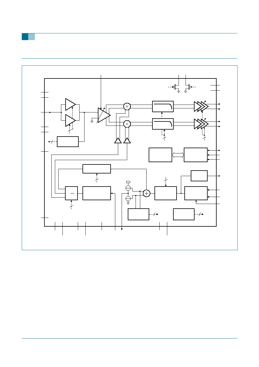
Block diagram
Fig 1.
Block diagram
3
3, 2
1
5
15
1
3
I
2
C-BUS
INTERFACE
LATCH
AND
CONTROL BIT
LOW-NOISE
INTEGRATED
LC OSCILLATOR
I/Q outputs
wide band
integrated
oscillator
XTOUT
CRYSTAL
OSCILLATOR
REFERENCE
DIVIDER
POWER-ON
RESET
1
3
LOCK
DETECTOR
LEVEL
DETECTOR
15-BIT DIVIDER
001aaa974
TDA8263HN
AS
V
CC(RF)
PORT0
CAPVCO
n.c.
V
CC(VCO)
GND(RF)
VT
V
CC(LNA)
GND(VCO)
RFIN
CP
GND(LNA)
V
CC(PLL)
GND(DIE)
GND(PLL)
V
CC(BB)
QP
QN
IN
IP
GND(BB)
MS
PORT1
GND(DIG)
SCL
SDA
XTN
XT
XTOUT
8
17
7
18
6
19
5
20
4
21
3
22
2
23
1
24
AGC
9
10
11
12
13
14
15
16
32
31
30
29
V
CC(DIG)
28
27
26
25
N2
N1
�
AGC
control
0
�
90
�
5 MHz to 36 MHz filter
0 dB to +9 dB
variation gain
LNA
ATT

9397 750 13193
� Koninklijke Philips Electronics N.V. 2004. All rights reserved.
Product data sheet
Rev. 01 -- 14 December 2004
5 of 28
Philips Semiconductors
TDA8263HN
Fully integrated satellite tuner
8.
Pinning information
8.1 Pinning
8.2 Pin description
Fig 2.
Pin configuration
001aaa976
TDA8263HN
Transparent top view
AS
V
CC(RF)
PORT0
CAPVCO
n.c.
V
CC(VCO)
GND(RF)
VT
V
CC(LNA)
GND(VCO)
RFIN
CP
GND(LNA)
V
CC(PLL)
GND(DIE)
GND(PLL)
AGC
V
CC(BB)
QP
QN
IN
IP
GND(BB)
MS
PORT1
GND(DIG)
SCL
SDA
V
CC(DIG)
XTN
XT
XTOUT
8
17
7
18
6
19
5
20
4
21
3
22
2
23
1
24
9
10
11
12
13
14
15
16
32
31
30
29
28
27
26
25
terminal 1
index area
Table 3:
Pin description
Symbol
Pin
Description
GND(DIE)
1
isolation ground
GND(LNA)
2
LNA ground
RFIN
3
RF input
V
CC(LNA)
4
LNA supply voltage
GND(RF)
5
RF ground
n.c.
6
not connected
V
CC(RF)
7
RF supply voltage
PORT0
8
pull-down port 0
AGC
9
automatic gain control input
V
CC(BB)
10
baseband supply voltage
QP
11
Q positive output
QN
12
Q negative output
IN
13
I negative output
IP
14
I positive output
GND(BB)
15
baseband ground
MS
16
master/slave crystal oscillator mode input
AS
17
address select input
CAPVCO
18
internal LC VCO regulation capacitor
Document Outline