 | –≠–ª–µ–∫—Ç—Ä–æ–Ω–Ω—ã–π –∫–æ–º–ø–æ–Ω–µ–Ω—Ç: TDA8303 | –°–∫–∞—á–∞—Ç—å:  PDF PDF  ZIP ZIP |

DATA SHEET
Preliminary specification
File under Integrated Circuits, IC02
July 1992
INTEGRATED CIRCUITS
TDA8303
TDA8303A
Small signal combination IC for
black/white TV

July 1992
2
Philips Semiconductors
Preliminary specification
Small signal combination IC for black/white TV
TDA8303
TDA8303A
FEATURES
∑
Video IF amplifier with synchronous demodulator
∑
Automatic gain control (AGC) detector suitable for
negative modulation
∑
AGC tuner
∑
Automatic frequency control (AFC) circuit with
sample-and-hold
∑
Video preamplifier
∑
Sound IF amplifier and demodulator
∑
DC volume control or separate supply for starting the
horizontal oscillator
∑
Audio preamplifier
∑
Horizontal synchronization circuit with two control loops
∑
Vertical synchronization (divider system) and sawtooth
generation with automatic amplitude adjustment for 50
and 60 Hz
∑
Transmitter identification (mute)
GENERAL DESCRIPTION
The TDA8303/TDA8303A combines all small signal
functions (except the tuner) which are required for a
monochrome television receiver. For a complete black and
white receiver only the output stages for video, sound,
horizontal and vertical deflection and a tuner have to be
added.
The TDA8303 is for applications with npn tuners and the
TDA8303A for pnp tuners.
FUNCTIONAL DESCRIPTION
Video IF amplifier, demodulator and video amplifier
Each of the three AC-coupled IF stages permits the
omission of DC feedback and possesses a control range
in excess of 20 dB. An additional advantage is the
symmetry of the amplifier which results in a less critical
application.
The IF amplifier is followed by a passive synchronous
demodulator providing a regenerated carrier signal. This is
limited by a logarithmic limiter circuit prior to its application
to the demodulator. The limiter has a very low differential
phase shift which results in good differential gain and
phase figures.
The video amplifier also contains a white spot inverter and
a noise clamp which limits interference pulses to a point
below the peak sync level. This circuit is more effective
than a noise inverter and results in an improved picture
stability, with respect to interference.
AFC-circuit
The reference signal for the AFC circuit is obtained from
the demodulator tuned circuit. In this way only one tuned
circuit needs to be applied and only one adjustment has to
be carried out. The disadvantage with this method is that
the frequency spectrum of the signal fed to the detector is
determined by the SAW filter characteristic. This spectrum
is asymmetrical with respect to the picture carrier so that
the AFC output voltage is dependent on the video signal.
To overcome this video frequency dependency of the AFC
output, the demodulator output is followed by a
sample-and-hold circuit which samples during the sync
level of the signal. This means that only the carrier signal
is available to the AFC and it will not be affected by the
video information.
At very weak input signals the drive signal of the AFC
circuit will contain substantial noise. This noise has an
asymmetrical frequency spectrum causing an offset in the
AFC output voltage. This effect can be minimized by
applying a notch in the demodulator tuned circuit. The
sample-and-hold circuit is followed by an amplifier with
high output impedance, therefore the steepness of the of
the AFC control voltage is dependent on the load
impedance.
ORDERING INFORMATION
Note
1. SOT117-1; 1996 December 3.
EXTENDED TYPE
NUMBER
PACKAGE
PINS
PIN POSITION
MATERIAL
CODE
TDA8303
28
DIL
plastic
SOT117
(1)
TDA8303A
28
DIL
plastic
SOT117
(1)
July 1992
3
Philips Semiconductors
Preliminary specification
Small signal combination IC for black/white TV
TDA8303
TDA8303A
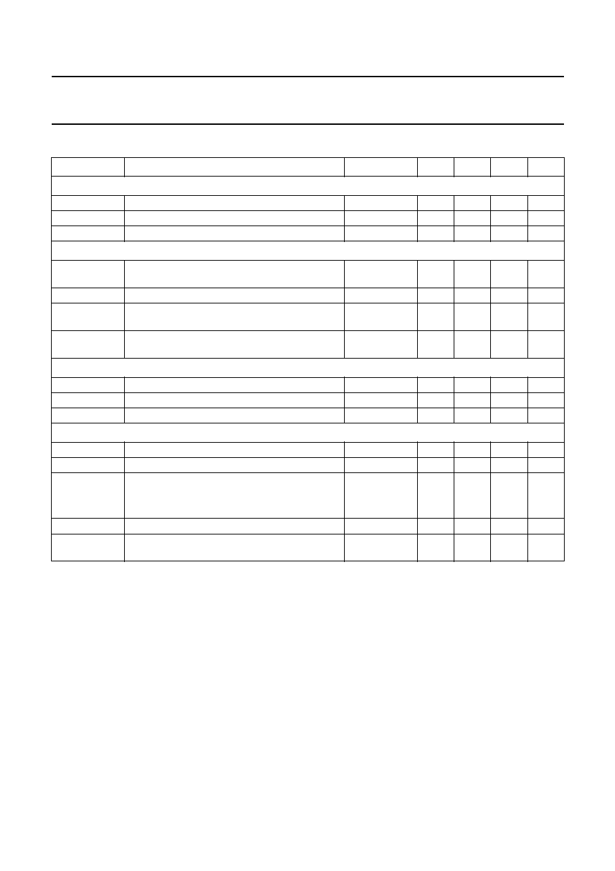
QUICK REFERENCE DATA
Notes to the quick reference data
1. Pin 11 has a double function. When during switch-on a current of 9 mA is supplied to this pin, it is used to start the
horizontal oscillator. The main supply can then be obtained from the horizontal deflection stage. When no current is
supplied to this pin it can be used as a volume control.
2. On set AGC.
3. The output signal is measured at
f = 7.5 kHz and maximum volume control.
4. The minimum value is obtained by connecting a 1.8 k
resistor and a 470 nF capacitor in series between the video
output and pin 25. The slicing level can be varied by changing the value of this resistor (higher resistance value
results in a larger value of the minimum sync pulse amplitude). The slicing level is independent of the video
information.
SYMBOL
PARAMETER
CONDITIONS
MIN.
TYP.
MAX.
UNIT
Supply
V
P
positive supply voltage (pin 7)
9.5
12
13.2
V
I
P
supply current (pin 7)
90
125
160
mA
I
start
start current (pin 11)
note 1
-
6.5
9
mA
Video
V
8-9(RMS)
IF sensitivity (RMS value)
at 38.9 MHz;
note 2
20
40
65
µ
V
G
8-9
IF gain control range
-
74
-
dB
S/N
signal-to-noise ratio
input signal =
10 mV
-
57
-
dB
V
18(p-p)
AFC output voltage swing
(peak-to-peak value)
10.5
-
11.5
V
Sound
V
12(RMS)
AF output signal (RMS value)
note 3
400
600
800
mV
AMS
AM suppression
at V
I
= 50 mV
-
58
-
dB
THD
total harmonic distortion
-
0.5
-
%
Sync
V
25
required sync pulse amplitude
note 4
200
-
-
mV
I
27
required input current during flyback pulse
0.1
-
2
mA
V
22
coincidence detector output voltage
in synchronized condition
-
9.7
-
V
in no signal condition
-
1.5
-
V
V
22
vertical feedback for DC voltage
2.9
3.3
3.7
V
V
22(p-p)
vertical feedback for AC voltage
(peak-to-peak value)
-
1.2
-
V

July 1992
4
Philips Semiconductors
Preliminary specification
Small signal combination IC for black/white
TV
TDA8303
TDA8303A
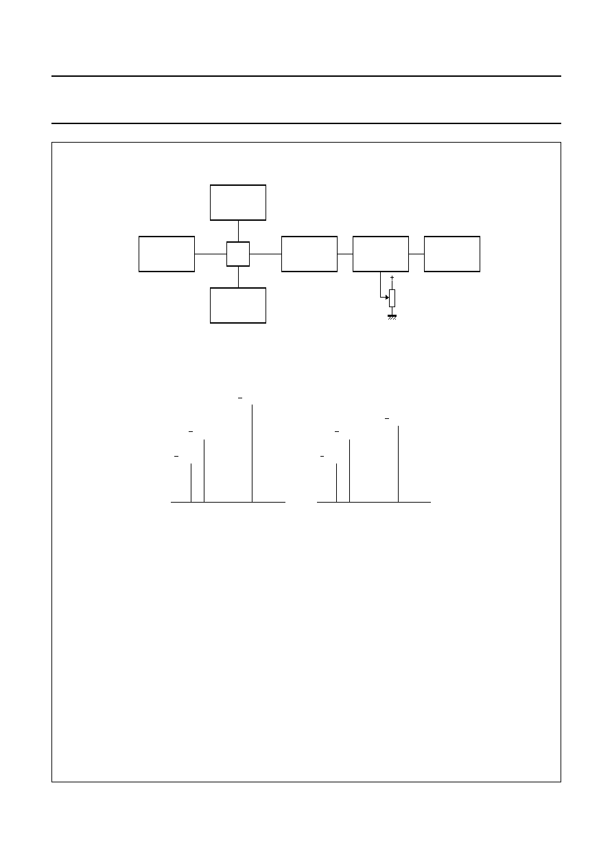
Fig.1 Block diagram

July 1992
5
Philips Semiconductors
Preliminary specification
Small signal combination IC for black/white
TV
TDA8303
TDA8303A
PINNING
AGC circuit
The AGC circuit of the TDA8303/TDA8303A is a top-sync
detector. The video signal coming from the video amplifier
passes a 2nd order low-pass filter before it is compared
with an internal reference level. The comparator stage is
gated when the horizontal oscillator is synchronized with
the video signal, such that interference pulses outside the
gating time have no influence on the gain control.
PIN
DESCRIPTION
1
AGC take-over
2
vertical ramp generator
3
vertical drive
4
vertical feedback
5
tuner AGC
6
ground
7
supply voltage input
8
video IF input
9
video IF input
10
IF AGC
11
volume control/start horizontal oscillator
12
audio output
13
sound demodulator
14
sound IF decoupling
15
sound IF input
16
ground (for some critical parts)
17
video amplifier output
18
AFC output
19
AFC S/H, AFC switch
20
video demodulator tuned circuit
21
video demodulator tuned circuit
22
coincidence detector
23
horizontal oscillator
24
phase 1 detector
25
sync separator input
26
horizontal drive output
27
horizontal flyback input
28
phase 2 detector
Sound circuit
The sound quality of the TDA8303/TDA8303A compared
with the predecessors has been improved at weak signal
conditions. The improvement has been achieved by the
new IF amplifier which is less sensitive for radiation from
the sound IF amplifier and by change of the ground and
supply connections in the IC. When out-of-sync condition
is detected by the coincidence detector the sound output
is muted. When no mute is required the minimum voltage
level on pin 22 should be clamped to a high level of 5 V.
At this level the gating of the AGC is switched off and the
phase 1 detector has a high output current for reliable
catching of a new transmitter.
Vertical synchronization
The TDA8303/TDA8303A embodies a synchronized
divider system for generating the vertical sawtooth at pin 2
having several advantages and features such as:
∑
The vertical frequency is alignment free. The divider
automatically adapts to a vertical frequency of 50 Hz or
60 Hz including automatic amplitude correction and its
operating modes offer maximum
interference/disturbance protection.
∑
A discriminator-window checks the accuracy of the
vertical trigger pulse. Internally clock pulses are
generated by doubling the line frequency. The divider
operates in the 60 Hz mode when the trigger pulse
appears before count 576, otherwise the 50 Hz mode
will be active.
∑
The divider system operates with two different reset
windows for maximum interference/disturbance
protection. The windows are activated via an up/down
counter. The counter increases its counter-value by 1 for
each time the separated vertical sync pulse appears
within the selected window, otherwise the counter value
is decreased by 1.
Modes of operation
Large search window: divider ratio between 488 and 576.
This mode is valid for the following conditions:
∑
Divider is looking for a new transmitter
∑
Divider ratio found does not comply with the narrow
window specification limits
∑
Up/down counter value of the divider system, operating
in the narrow window mode, drops below count 10

July 1992
6
Philips Semiconductors
Preliminary specification
Small signal combination IC for black/white TV
TDA8303
TDA8303A
Narrow window mode: divider ratio between 522 and 528
(60 Hz); or 622 and 628 (50 Hz).
∑
The divider system switches over to narrow window
mode when the up/down counter has reached his
maximum value of 15 approved vertical sync pulses
∑
When the divider operates in the narrow window mode
and a vertical sync pulse is missing within the window,
the divider is reset at the end of that window and the
counter value is decreased by 1
∑
At a counter value below 10 the divider system switches
over to the large window mode
∑
The divider system also generates an anti-top-flutter
pulse which inhibits the phase 1 detector during the
vertical sync pulse. The pulse width is dependent on the
divider mode. For the large window mode the start is
generated at the reset of the divider. In the narrow
window mode the anti-top-flutter pulse starts at the
beginning of the first equalizing pulse. The
anti-top-flutter pulse ends at count 10 for the 50 Hz
mode and count 12 for the 60 Hz mode
VCR switch
An extra time constant switch in the horizontal phase
detector makes an external VCR switch redundant. The
time constant is automatically switched depending on the
signal strength of the IF input (pins 8/9) and the
coincidence detector.
When a strong signal is detected (V
8/9
>
2.2 mV) and the
circuit is synchronized the time constant of the phase
detector is optimum for VCR playback, a fast time constant
during the vertical retrace to correct head errors of the
VCR and during scan a sufficient time constant to correct
fluctuations of the horizontal sync
During weak signal and synchronized conditions the time
constant is enlarged and the phase detector is gated. This
ensures a stable display which is not disturbed by the
noise in the video signal. When the circuit is not
synchronized the time constant is fast and not gated to
ensure a short catching time.
Combination of DC volume control and start-up
feature
Pin 11 of the IC can be used as a DC volume control or as
a start-up feature of the horizontal oscillator/output circuit
dependent on the application.
Volume control is achieved by connecting a 4.7 k
potentiometer or a DC voltage of 0 to 3 V to pin 11. When
a current of 9 mA is supplied to pin 11 the volume control
is set to a fixed output signal level and the circuit will
generate drive pulses for the horizontal deflection and the
main supply can be derived from the deflection.
Application when external video signals require
synchronization
The input to the sync separator is externally available via
pin 25. For normal application the video output signal at pin
17 is AC-coupled to the sync separator input. It is possible
to interrupt this connection and drive the sync separator
from other sources.
When external signals are applied to the sync separator
the connections between the two parts must be
interrupted. This can be achieved by connecting pin 22 to
ground, which results in the following conditions:
∑
AGC detector is not gated
∑
Mute circuit not active, sound channel remains switched
on
∑
Phase detector 1 has an optimum time constant for
external video sources and is not gated
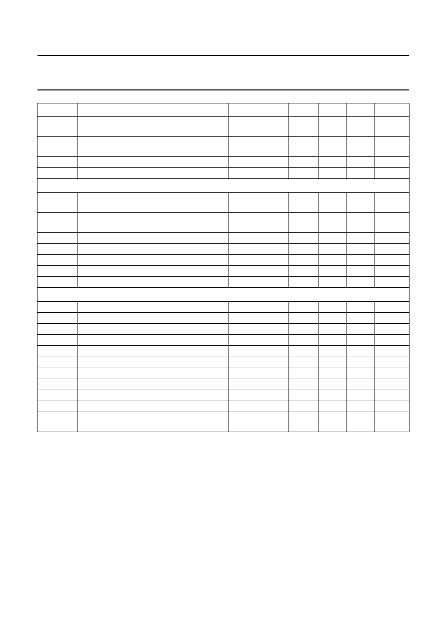
LIMITING VALUES
In accordance with the Absolute Maximum System (IEC 134)
SYMBOL
PARAMETER
MIN.
MAX.
UNIT
V
P
supply voltage (pin 7)
-
13.2
V
P
tot
total power dissipation
-
2.3
W
T
stg
storage temperature range
-
55
+150
∞
C
T
amb
operating ambient temperature range
-
25
+65
∞
C

July 1992
7
Philips Semiconductors
Preliminary specification
Small signal combination IC for black/white TV
TDA8303
TDA8303A
CHARACTERISTICS
V
P
= 12 V;T
amb
= 25
∞
C; carrier 38.9 MHz negative modulation, unless otherwise specified
SYMBOL
PARAMETER
CONDITIONS
MIN.
TYP.
MAX.
UNIT
Supply (pin 7)
V
P
supply voltage range
9.5
12
13.2
V
I
P
supply current
no input
90
125
160
mA
I
11
start current (pin 11)
note 1
-
6.5
9
mA
V
11
start voltage horizontal oscillator
9.5
-
-
V
V
11
start protection level
I
11
= 12 mA
-
-
16.5
V
IF Amplifier (pins 8 and 9)
V
8-9(RMS)
input sensitivity (RMS value)
at 38.9 MHz;
note 2
25
40
65
µ
V
V
8-9(RMS)
input sensitivity (RMS value)
at 45.75 MHz;
notes 2 and 25
25
40
65
µ
V
R
8-9
differential input resistance
note 3
-
1300
-
C
8-9
differential input capacitance
note 3
-
5
-
pF
G
8-9
gain control range
-
74
-
dB
V
17
output signal expansion for 46 dB input signal
variation
note 4
-
1
-
dB
V
8-9
maximum input signal
100
170
-
mV
Video Amplifier (note 5)
V
17
zero signal output level
note 6
-
5.4
-
V
V
17
peak sync level
2.3
2.5
2.7
V
V
17
video output signal amplitude
note 7
2.3
2.65
3.0
V
V
17
white spot threshold level
-
5.7
-
V
V
17
white spot insertion level
-
3.8
-
V
Z
17
video output impedance
-
25
-
I
17
internal bias current of npn emitter follower
output transistor
1.4
1.8
-
mA
I
source
maximum source current (pin 17)
10
-
-
mA
B
bandwidth of demodulated output signal
5
7
-
MHz
G
17
differential gain
note 8
-
4
8
%
differential phase
note 8
-
2
5
deg.
NL
video non linearity
note 9
-
2
5
%
intermodulation
note 10
1.1 MHz; blue
50
60
-
dB
1.1 MHz; yellow
50
60
-
dB
3.3 MHz; blue
55
65
-
dB
3.3 MHz; yellow
55
65
-
dB
July 1992
8
Philips Semiconductors
Preliminary specification
Small signal combination IC for black/white TV
TDA8303
TDA8303A
S/N
signal-to-noise ratio
10 mV input
signal
50
57
-
dB
S/N
signal-to-noise ratio
end of gain
control range
50
62
-
dB
V
17
residual carrier signal
-
2
10
mV
V
17
residual 2nd harmonic of carrier signal
-
2
10
mV
Tuner AGC
V
8-9(RMS)
minimum starting point for tuner take
-
over
(RMS value)
-
-
0.2
mV
V
8-9(RMS)
maximum starting point for tuner take
-
over
(RMS value)
100
150
-
mV
I
5
maximum tuner AGC output swing
V
5
= 3 V
4
-
-
mA
V
5
output saturation voltage
I
5
= 2 mA
-
-
300
mV
I
L
leakage current (pin 5)
-
-
1
µ
A
V
I
input signal variation complete tuner control
0.2
2
4
dB
V
1
minimum voltage tuner take
-
over
-
-
1
V
AFC circuit
I
19
AFC sample-and-hold switch-off current
0.1
-
-
mA
I
O
output current (pin 19)
V
19
= 0 V
-
0.1
0.3
mA
I
LO
output leakage current (pin 19)
-
-
2
µ
A
V
18
AFC output voltage swing
notes 18 and 19
10.5
-
11.5
V
I
18
available output current
0.2
-
-
mA
control slope
-
100
-
mV/kHz
V
O
output voltage (pin 18)
AFC off
5.5
6
6.5
V
R
O
AFC output resistance
-
40
-
k
V
18
output voltage swing
notes 25 and 26
-
11
-
V
control slope
notes 25 and 26
-
80
-
mV/kHz
V
18
output voltage shift with respect to
V
I
= 10 mV(RMS)
notes 25 and 26
-
-
2
-
V
SYMBOL
PARAMETER
CONDITIONS
MIN.
TYP.
MAX.
UNIT
July 1992
9
Philips Semiconductors
Preliminary specification
Small signal combination IC for black/white TV
TDA8303
TDA8303A
Sound circuit (note 12)
V
15
input limiting voltage
V
O(max)
=
-
3 dB
-
400
800
µ
V
R
15
input resistance
-
2.6
-
k
C
15
input capacitance
-
6
-
pF
AMS
AM suppression
note 13
53
58
-
dB
V
12(RMS)
AF output signal (RMS value)
note 14
400
600
800
mV
V
12(RMS)
AF output signal when pin 11 is used as a
starting pin or connected to V
P
(RMS value)
f = 50 kHz
500
900
1500
mV
Z
12
AF output impedance
-
25
100
THD
total harmonic distortion
note 15
-
0.5
2
%
RR
ripple rejection
volume control
-
20 dB;
f
k
= 100 Hz
-
35
-
dB
V
12
output voltage when muted
-
2.5
-
V
V
12
output level shift due to muting
volume control
-
20 dB
-
-
0.5
dB
S/N
signal-to-noise ratio
note 16
-
47
-
dB
V
11
voltage with pin 11 disconnected
-
6
-
V
I
11
current with pin 11 short-circuited to ground
-
1
-
mA
V
12
temperature dependence of the output signal
amplitude
T
amb
= 20 to 65
∞
C;
-
30 dB volume
control and
voltage of pin 11
fixed;
note 17
-
2.5
-
dB
Volume control (note 17; see Fig.8)
R
11
external control resistor
note 17
-
4.7
-
k
OSS
suppression of output signal during mute
condition
60
66
-
dB
Horizontal synchronization circuit (see Fig.9)
S
YNC SEPARATOR
V
25
required sync pulse amplitude
note 20
200
750
-
mV
I
25
input current (pin 25)
V
25
>
5 V
-
8
-
µ
A
V
25
= 0 V
-
10
-
mA
F
IRST CONTROL LOOP
±
f
PLL holding range
-
1500
2000
Hz
±
f
PLL catching range
600
1500
-
Hz
control sensitivity to oscillator
note 21
see Fig.10
V
8-9
IF input signal at which the time constant is
switched (RMS value)
strong-to-weak
-
2.2
-
mV
SYMBOL
PARAMETER
CONDITIONS
MIN.
TYP.
MAX.
UNIT

July 1992
10
Philips Semiconductors
Preliminary specification
Small signal combination IC for black/white TV
TDA8303
TDA8303A
S
ECOND CONTROL LOOP
(
POSITIVE EDGE
)
control sensitivity
note 22
-
100
-
t
d
control range
-
25
-
µ
s
P
HASE ADJUSTMENT
(
VIA SECOND CONTROL LOOP
)
control sensitivity
-
25
-
µ
A/
µ
s
maximum allowed phase shift
-
±
2
-
µ
s
H
ORIZONTAL OSCILLATOR
f
fr
free running frequency
R = 34.3 k
;
C = 2.7 nF
-
15625
-
Hz
f
spread with fixed external components
-
-
4
%
f
fr
frequency variations with supply voltage from
9.5 to 13.2 V
-
-
2
%
f
T
frequency variation with temperature
note 25
-
-
1.6
-
Hz/
∞
C
f
fr
maximum frequency deviation at start of
horizontal output
-
-
10
%
f
frequency variation when only noise is
received
note 25
-
-
500
Hz
H
ORIZONTAL OUTPUT
(
PIN
26;
OPEN COLLECTOR
)
V
26
output limiting voltage
-
-
16.5
V
V
OL
LOW level output voltage
I
sink
= 10 mA
-
0.2
0.5
V
I
sink
maximum sink current
10
-
-
mA
duty factor of output signal
-
46
-
%
t
r
rise time of output pulse
-
260
-
ns
t
f
fall time of output pulse
-
100
-
ns
H
ORIZONTAL FLYBACK INPUT
(
PIN
27)
I
27
required input current during flyback pulse
0.01
-
1.0
mA
C
OINCIDENCE DETECTOR
V
22
voltage for in-sync condition
-
9.8
-
V
V
22
voltage for no-sync condition
no signal
-
1.5
-
V
V
22
switching level to the phase detector from fast
to slow
6.2
6.7
7.2
V
V
22
hysteresis slow to fast
-
0.6
-
V
V
22
switching level to activate the mute function
(transmitter identification)
2.5
2.8
3.1
V
V
22
hysteresis mute function
-
2
-
V
t
d
delay of mute release after transmitter
insertion
-
-
300
µ
s
allowable load on pin 22
-
-
10
µ
A
V
22
external video mode
-
-
0.7
V
I
22
current at pin 22
V
22
= 0 V
-
-
0.8
mA
SYMBOL
PARAMETER
CONDITIONS
MIN.
TYP.
MAX.
UNIT
t
d
t
o
-------

July 1992
11
Philips Semiconductors
Preliminary specification
Small signal combination IC for black/white TV
TDA8303
TDA8303A
Notes to the characteristics
1. Pin 11 has a double function. When during switch-on a current of 9 mA is supplied to this pin, it is used to start the
horizontal oscillator. The main supply can then be obtained from the horizontal deflection stage. When no current is
supplied to this pin it can be used as a volume control.
2. On set AGC.
3. The input impedance has been chosen such that a SAW filter can be employed.
4. Measured with 0 dB = 450
µ
V.
5. Measured at 10 mV RMS top sync input signal.
6. Projected zero point; i.e. with switched demodulator.
7. White 10% of the top sync amplitude.
8. Measured according to the test line illustrated by Fig.2. The differential gain is expressed as a percentage of the
difference in peak amplitudes between the largest and smallest value relative to the subcarrier amplitude at blanking
level. The differential phase is defined as the difference in degrees between the largest and smallest phase angle.
The differential gain and phase are measured with a DSB signal.
9. This figure is valid for the complete video signal amplitude (peak white-to-black); see Fig.3. The non
-
linearity is
expressed as a percentage of the maximum deviation of a luminance step from the mean step, with respect to the
mean step.
10. The test set
-
up and input conditions are illustrated by Fig.4. The figures are measured at an input signal of 10 mV
RMS.
11. Measured with a source impedance of 75
.
12. The sound circuit is measured (unless otherwise specified) with an input signal of V
15
of 50 mV RMS, a carrier
frequency of 5.5 MHz at a
f of 27.5 kHz. The QL of the demodulator tuned circuit is 16 and the volume control is
Vertical circuit (note 24)
V
ERTICAL RAMP GENERATOR
I
2
input current during scan
-
-
2
µ
A
I
2
discharge current during retrace
-
0.8
-
mA
V
2(p
-
p)
sawtooth amplitude (peak-to-peak value)
-
1.9
-
V
t
interlace timing of the internal pulses
30
32
34
µ
s
V
ERTICAL OUTPUT
I
3
available output current
V
3
= 4 V
-
-
3
mA
V
3
maximum available output voltage
I
3
= 0.1 mA
4.4
5
-
V
V
ERTICAL FEEDBACK INPUT
V
4
DC input voltage
2.9
3.3
3.7
V
V
4(p
-
p)
AC input voltage (peak-to-peak value)
-
1
-
V
I
4
input current
-
-
12
µ
A
t
p
internal pre-correction to sawtooth
-
3
-
%
deviation amplitude
50/60 Hz
-
-
4
%
temperature dependency of the amplitude
T
amb
= 20 to
65
∞
C
-
-
2
%
SYMBOL
PARAMETER
CONDITIONS
MIN.
TYP.
MAX.
UNIT
The signal-to-noise ratio = 20
V
O
black-to-white
V
n RMS
(
)
at B = 5 MHz
-----------------------------------------------------------
log

July 1992
12
Philips Semiconductors
Preliminary specification
Small signal combination IC for black/white TV
TDA8303
TDA8303A
connected to the supply. The reference circuit must be tuned in such a way that the output is symmetrical clipping at
maximum volume.
13. The test set-up is illustrated by Fig.6. The AM rejection curve (typical) is illustrated by Fig.7.
14. The output signal is measured at a
f = 7.5 kHz and maximum volume control.
15. The demodulator tuned circuit must be tuned at minimum distortion.
16. Weighted noise, measured in accordance with CCIR 468.
17. See also note 1. The volume can be controlled by using a potentiometer connected to ground (value 4.7 k
) or by
means of a variable direct voltage. In the latter event the relatively low input impedance must be taken into account.
18. The AFC control voltage is obtained by multiplying the IF output signal (which is also used to drive the synchronous
demodulator) with a reference carrier. This reference carrier is obtained from the demodulator tuned circuit via a 90
degree phase shift network.The IF output signal has an asymmetrical frequency spectrum with respect to the carrier
frequency. To avoid problems due to this asymmetrical signal the AFC circuit is followed by a sample-and-hold circuit
which samples during the sync level. As a result the AFC output voltage contains no video information. The specified
control slope decreases when the AFC output is loaded with two resistors between the voltage supply and ground.
19. At very weak input signals the drive signal for the AFC circuit will have a high noise content. This noise input has an
asymmetrical frequency spectrum which will cause an offset of the AFC output voltage. The characteristics given for
weak signals are measured with a SAW filter (OFW 1956) connected in front of the IC input signal such that the input
signal of the IC is 150
µ
V RMS.
20. The minimum value is obtained by connecting a 1.8 k
resistor between pins 17 and 25. The slicing level can be
varied by changing the value of this resistor (higher resistor value results in larger value of the minimum sync pulse
amplitude). The slicing level is independent of the video information.
21. Frequency control is obtained by supplying a correction current to the oscillator RC network via a resistor connected
between the phase 1 detector output and the oscillator network. The oscillator can be adjusted to the correct
frequency by short circuiting the sync separator bias network (pin 25) to the voltage supply. To avoid the need of a
VCR switch the time constant of the phase detector at strong input signals is sufficiently short to obtain a stable
picture during VCR playback. During the vertical retrace period the time constant is even shorter so that the
head
-
errors of the VCR are compensated at the beginning of scan. During conditions of weak signal (information
derived from the AGC circuit) the time constant is increased to obtain a better noise immunity.
22. This figure is valid for an external load impedance of 82 k
between pin 28 and the phase adjustment potentiometer.
23. The functions in-sync/out-of-sync and transmitter identification have been combined on pin 22. The capacitor is
charged during the sync pulse and discharged during the time difference between gating (6.5
µ
s) and the sync pulse.
24. The vertical scan is synchronized by means of a divider system. Therefore no frequency adjustment is required for
the ramp generator. The divider detects whether the incoming signal has a vertical frequency of 50 or 60 Hz and
corrects the vertical amplitude.
25. These figures are based on test samples.
26. Measured at an input signal amplitude of 150
µ
V RMS (pin 18).

July 1992
13
Philips Semiconductors
Preliminary specification
Small signal combination IC for black/white TV
TDA8303
TDA8303A
Fig.2 Video output signal.
handbook, full pagewidth
MLA667
100%
95%
30%
17.5%
Fig.3 EBU test signal waveform (line 330).
handbook, full pagewidth
MBC211
100%
86%
72%
58%
44%
30%
64
60
56
52
48
44
40
36
32
22
12
10
26
µ
s
July 1992
14
Philips Semiconductors
Preliminary specification
Small signal combination IC for black/white TV
TDA8303
TDA8303A
Fig.4 Test set-up intermodulation.
Input signal conditions
SC = Sound carrier
CC = Chrominance carrier
PC = Picture carrier
All with respect to top sync level
Value at 1.1 MHz : 20 log
V
O
at 4.4 MHz
V
O
at 1.1 MHz
--------------------------------------
3.6 dB
+
Value at 3.3 MHz : 20 log
V
O
at 4.4 MHz
V
O
at 3.3 MHz
--------------------------------------
handbook, full pagewidth
MLA666
ATTENUATOR
SPECTRUM
ANALYZER
TEST
CIRCUIT
CC
34.5 MHz
PC
38.9 MHz
SC
33.4 MHz
gain setting adjusted
for blue or yellow
handbook, full pagewidth
MBC213
SC CC
PC
30 dB
13.2 dB
3.2 dB
SC CC
PC
30 dB
13.2 dB
10 dB
BLUE
YELLOW

July 1992
15
Philips Semiconductors
Preliminary specification
Small signal combination IC for black/white TV
TDA8303
TDA8303A
Fig.5
Signal-to-noise ratio as a function of the
input voltage (0 dB = 100 mV).
Fig.6 Test set-up AM suppression.
July 1992
16
Philips Semiconductors
Preliminary specification
Small signal combination IC for black/white TV
TDA8303
TDA8303A
Fig.7 AM suppression.
Fig.8 Volume control characteristics.

July 1992
17
Philips Semiconductors
Preliminary specification
Small signal combination IC for black/white TV
TDA8303
TDA8303A
Fig.9 Timing diagram.
July 1992
18
Philips Semiconductors
Preliminary specification
Small signal combination IC for black/white TV
TDA8303
TDA8303A
Table 1
Switching levels coincidence detector
CONDITION
V
22
CONTROL SENSITIVITY
HORIZONTAL OSCILLATOR (kHz/
µ
S)
T2 - T1
T3 = SCAN
V
22
>
6.7 V
and
strong signal
11.3
7.6
weak signal
1.3
1.3
1
<
V
22
<
5.7 V
and
strong signal
11.3
7.6
weak signal
11.3
7.6
V
22
<
0.7
11.3
7.6
Fig.10 Switching levels coincidence detector.
Fig.11 Anti-top-flutter pulse.
July 1992
19
Philips Semiconductors
Preliminary specification
Small signal combination IC for black/white TV
TDA8303
TDA8303A
Fig.12 Application diagram.

July 1992
20
Philips Semiconductors
Preliminary specification
Small signal combination IC for black/white TV
TDA8303
TDA8303A
PACKAGE OUTLINE
UNIT
A
max.
1
2
b
1
(1)
(1)
(1)
c
D
E
w
e
M
H
L
REFERENCES
OUTLINE
VERSION
EUROPEAN
PROJECTION
ISSUE DATE
IEC
JEDEC
EIAJ
mm
inches
DIMENSIONS (inch dimensions are derived from the original mm dimensions)
SOT117-1
92-11-17
95-01-14
A
min.
A
max.
b
Z
max.
M
E
e
1
1.7
1.3
0.53
0.38
0.32
0.23
36.0
35.0
14.1
13.7
3.9
3.4
0.25
2.54
15.24
15.80
15.24
17.15
15.90
1.7
5.1
0.51
4.0
0.066
0.051
0.020
0.014
0.013
0.009
1.41
1.34
0.56
0.54
0.15
0.13
0.01
0.10
0.60
0.62
0.60
0.68
0.63
0.067
0.20
0.020
0.16
051G05
MO-015AH
M
H
c
(e )
1
M
E
A
L
seating plane
A
1
w
M
b
1
e
D
A
2
Z
28
1
15
14
b
E
pin 1 index
0
5
10 mm
scale
Note
1. Plastic or metal protrusions of 0.25 mm maximum per side are not included.
handbook, full pagewidth
DIP28: plastic dual in-line package; 28 leads (600 mil)
SOT117-1

July 1992
21
Philips Semiconductors
Preliminary specification
Small signal combination IC for black/white TV
TDA8303
TDA8303A
SOLDERING
Introduction
There is no soldering method that is ideal for all IC packages. Wave soldering is often preferred when through-hole and
surface mounted components are mixed on one printed-circuit board. However, wave soldering is not always suitable for
surface mounted ICs, or for printed-circuits with high population densities. In these situations reflow soldering is often
used.
This text gives a very brief insight to a complex technology. A more in-depth account of soldering ICs can be found in our
"IC Package Databook" (order code 9398 652 90011).
Soldering by dipping or by wave
The maximum permissible temperature of the solder is 260
∞
C; solder at this temperature must not be in contact with the
joint for more than 5 seconds. The total contact time of successive solder waves must not exceed 5 seconds.
The device may be mounted up to the seating plane, but the temperature of the plastic body must not exceed the
specified maximum storage temperature (T
stg max
). If the printed-circuit board has been pre-heated, forced cooling may
be necessary immediately after soldering to keep the temperature within the permissible limit.
Repairing soldered joints
Apply a low voltage soldering iron (less than 24 V) to the lead(s) of the package, below the seating plane or not more
than 2 mm above it. If the temperature of the soldering iron bit is less than 300
∞
C it may remain in contact for up to
10 seconds. If the bit temperature is between 300 and 400
∞
C, contact may be up to 5 seconds.
DEFINITIONS
LIFE SUPPORT APPLICATIONS
These products are not designed for use in life support appliances, devices, or systems where malfunction of these
products can reasonably be expected to result in personal injury. Philips customers using or selling these products for
use in such applications do so at their own risk and agree to fully indemnify Philips for any damages resulting from such
improper use or sale.
Data sheet status
Objective specification
This data sheet contains target or goal specifications for product development.
Preliminary specification
This data sheet contains preliminary data; supplementary data may be published later.
Product specification
This data sheet contains final product specifications.
Limiting values
Limiting values given are in accordance with the Absolute Maximum Rating System (IEC 134). Stress above one or
more of the limiting values may cause permanent damage to the device. These are stress ratings only and operation
of the device at these or at any other conditions above those given in the Characteristics sections of the specification
is not implied. Exposure to limiting values for extended periods may affect device reliability.
Application information
Where application information is given, it is advisory and does not form part of the specification.