 | –≠–ª–µ–∫—Ç—Ä–æ–Ω–Ω—ã–π –∫–æ–º–ø–æ–Ω–µ–Ω—Ç: TDA8385 | –°–∫–∞—á–∞—Ç—å:  PDF PDF  ZIP ZIP |

March 1994
2
Philips Semiconductors
Preliminary specification
Control circuit for a Self-Oscillating
Power Supply (SOPS)
TDA8385
FEATURES
∑
Bandgap reference generator
∑
Slow-start circuitry
∑
Low-loss peak current sensing
∑
Over-voltage protection
∑
Hysteresis controlled stand-by
function
∑
Error amplifier with gain setting
∑
Programmable transfer character
generator
∑
Protection against open- and
short-circuited feedback loop
∑
Over-load current fold back
characteristic
∑
LED driver
∑
Demagnetization protection
∑
Programmable determination of
switch-on moment of switching
transistor for low-switching losses
∑
Feed-forward input
∑
Regulation-indicator output
∑
Programmable minimum on-time of
switching transistor
∑
Accurate peak-current setting.
GENERAL DESCRIPTION
The TDA8385 is intended to be used
in combination with the opto-coupler
(CNR50) as a control unit for a
self-oscillating power supply.
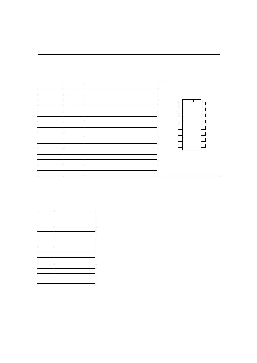
ORDERING INFORMATION
EXTENDED TYPE
NUMBER
PACKAGE
PINS
PIN POSITION
MATERIAL
CODE
TDA8385
16
DIL
plastic
SOT38WBE
March 1994
3
Philips Semiconductors
Preliminary specification
Control circuit for a Self-Oscillating
Power Supply (SOPS)
TDA8385
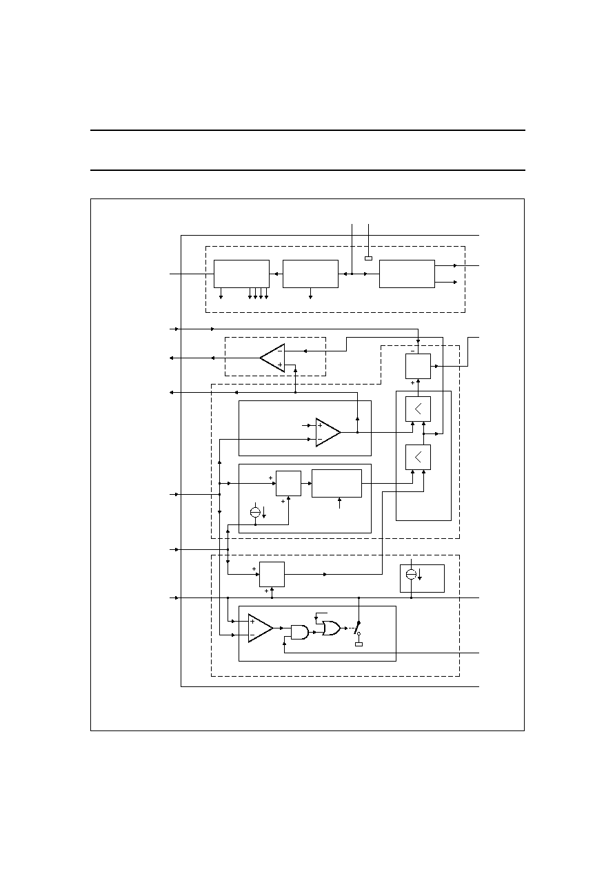
BLOCK DIAGRAMS
handbook, full pagewidth
MCD417
29
V ts
DIFFERENTIAL AMPLIFIER
CONTROL PART
REGULATION
INDICATOR
(2.5 V)
27
reset (28)
quick
discharge
CLAMP
50
µ
A
50
µ
A
charge
19
2.5 V
TCG
4
3
V TCG
V diff
Vss +
MINIMUM
VOLTAGE
CLAMP
6
X
III
VII
fo
V
Vmv
fb
V
13
1
RIO
11 V diff
9
4
7
Vss
7
16
14
3
REFERENCE
BLOCK
STABILIZED
SUPPLY
DETECTOR
VP (min)
28
1
2
SUPPLY REFERENCES
(28, 27, 23)
reset
latch
I ref
I ref
Vstab
Vref
Vref
I
current reference
setting
feed forward
input
regulation indicator
output
differential amplifier
output
slow start voltage
input
feedback voltage
input
transistor-on
setting input
VP
GND
SLOW START
V ts
5
Ton(min)
Ton (min)
Fig.1 Block diagram; part A (continued in Fig.2; part B).
March 1994
4
Philips Semiconductors
Preliminary specification
Control circuit for a Self-Oscillating
Power Supply (SOPS)
TDA8385
handbook, full pagewidth
stand-by voltage input
over-voltage
protection
latch
22
24
11
MCD418
100
µ
A
slow
discharge
21
(17)
(28)
VIII
Q
R
S
FF
23
over voltage
Q
115 mV
2.5 V
OVER-VOLTAGE PROTECTION
DELAY
12
115 mV
100 mV
SAWTOOTH GENERATOR
DEM
12
15
5
6
8
Q
13
R
S
Vr
Vsb
Vsim
8
PWM
IV
14
16
demagnetization
LED CONTROL
demagnetization
(28)
18
V
9
I12
12
0.2 I
I sim
I peak
25
2.5 V
2 V
STAND-BY
IX
2.5 V
latch
Q (23)
17
OUTPUT
STAGE
15
LED
LED DRIVER
VI
10
TDA8385
2
LED driver output
delay setting
demagnetization
input
peak-current
setting input
current simulation
input
26
comparator
II
V
c
10
FF
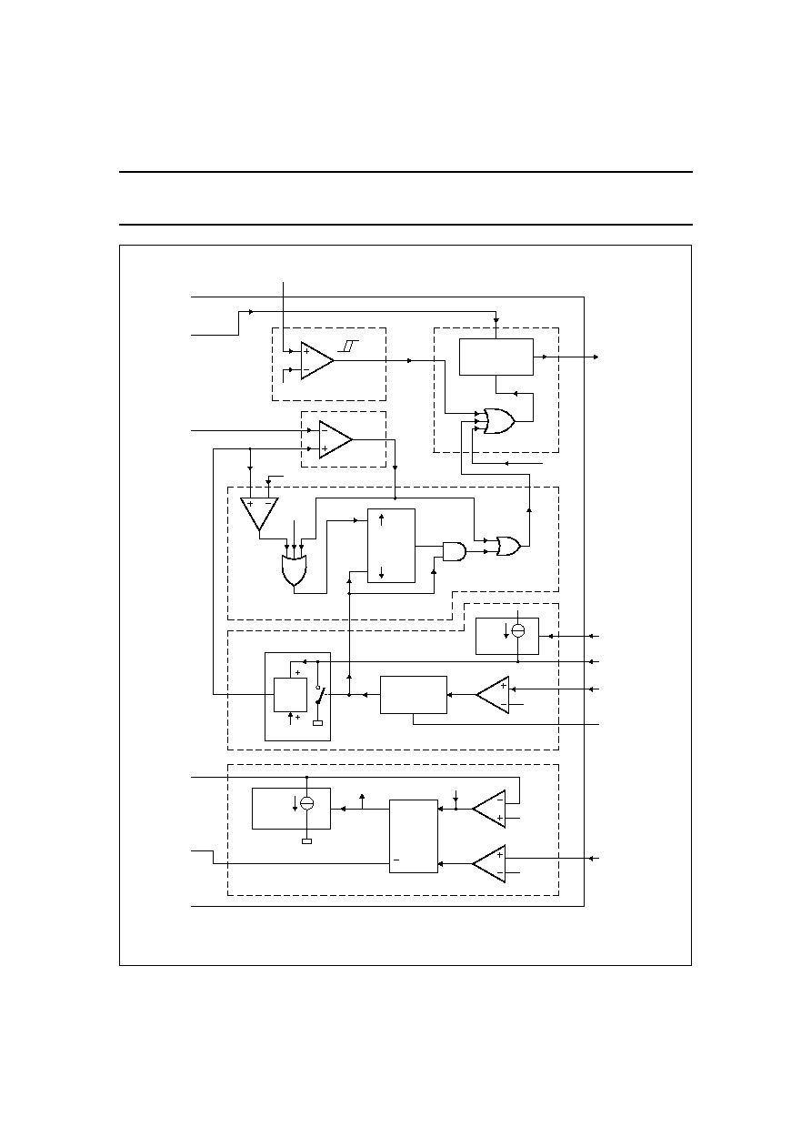
Fig.2 Block diagram; part B (continued from Fig.1; part A).
March 1994
5
Philips Semiconductors
Preliminary specification
Control circuit for a Self-Oscillating
Power Supply (SOPS)
TDA8385
PINNING
SYMBOL
PIN
DESCRIPTION
RIO
1
regulation indicator output
LED
2
LED driver output
I
ref
3
current reference setting
T
on(min)
4
transistor-on setting input
I
peak
5
peak current setting input
DELAY
6
delay setting
V
ss
7
slow start voltage input
OVP
8
over-voltage protection
V
fb
9
feedback voltage input
V
sb
10
stand-by voltage input
V
diff
11
differential amplifier output
I
sim
12
current simulation input
V
fo
13
feed forward input
GND
14
ground (0 V)
DEM
15
demagnetization input
V
P
16
positive supply voltage
Fig.3 Pinning diagram.
handbook, 2 columns
1
2
3
4
5
6
7
8
16
15
14
13
12
11
10
9
RIO
LED
DELAY
OVP
I ref
Ton(min)
I peak
Vss
DEM
GND
VP
Vfo
I sim
Vdiff
sb
V
fb
V
TDA8385
MCD402
FUNCTIONAL DESCRIPTION
The TDA8385 can be divided into
10 functional blocks as shown in Fig.1
and Fig.2.
Block for Figs 1 and 2
These 10 functional blocks of Fig.1
and Fig.2 contain sub-sections
numbered 1 to 28 which are
BLOCK
NO.
DESCRIPTION
I
supply references
II
sawtooth generator
III
control part
IV
pulse width modulator
(PWM)
V
LED control
VI
LED driver
VII
slow-start circuitry
VIII
over-voltage protection
IX
stand-by circuit
X
regulation-indicator
output
cross-referenced in the following
description.
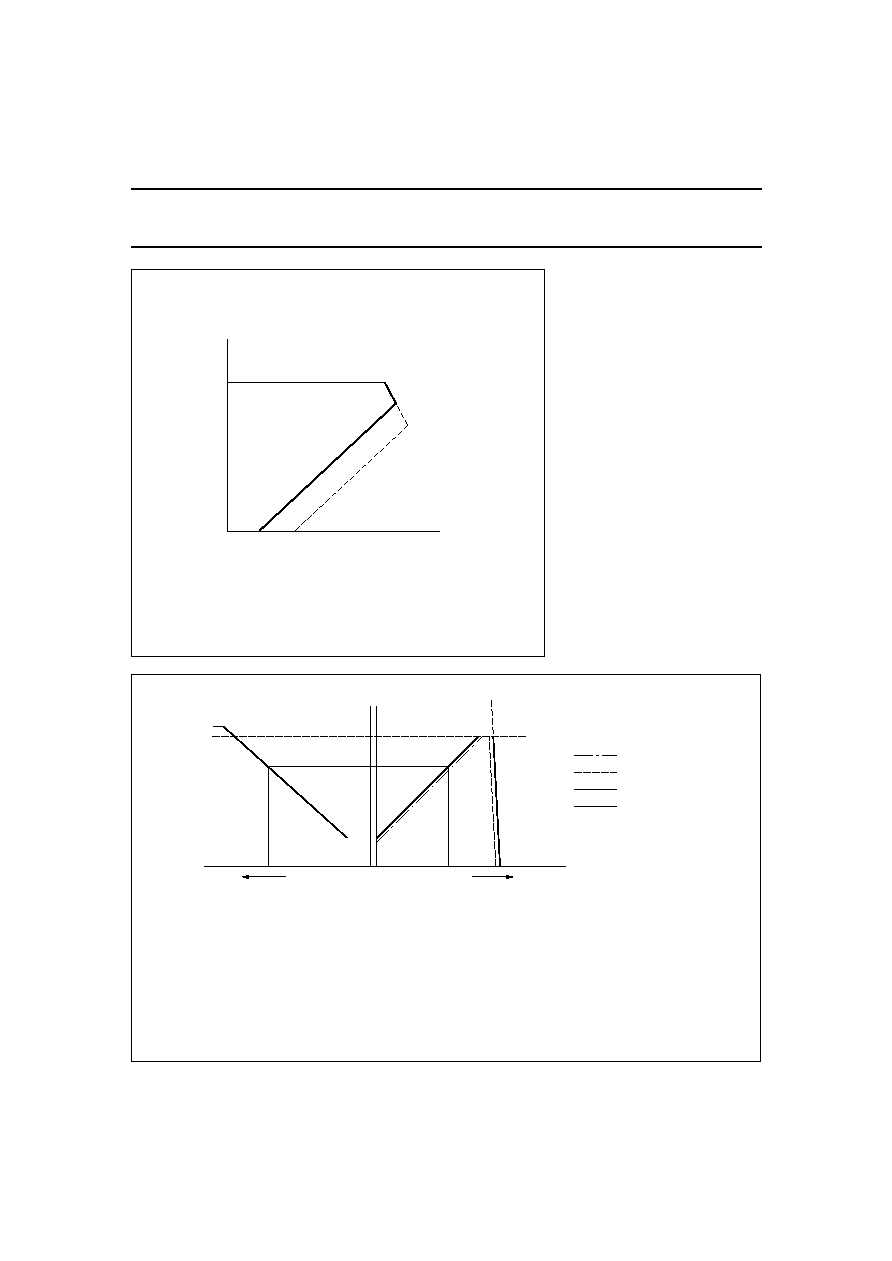
Supply references (Block I)
The TDA8385 is intended to be used
on the secondary side of the
self-oscillating power supply. It can be
supplied either by an auxiliary winding
of the transformer or an external
supply e.g. 50 Hz transformer.
Charging of the capacitor C
P
(see
Fig.16) takes place during transistor
on-time (T
on
; see Fig.17). During
stand-by the IC is supplied by the
stand-by voltage V
sb
(pin 10). The
operating voltage range is from 7.5 to
20 V. The supply current, inclusive
drive current for the LED, is less than
20 mA. A bandgap based reference
(2.5 V) generates a stabilized voltage
V
stab
of 3.9 V to supply all internal
circuits of the IC except the LED
driver. The LED driver is directly
supplied by V
P
. The reference block
generates all the reference voltages
in the circuit. By means of a resistor
connected to pin 3, a reference
current (I
ref
) is defined.
This current is reflected several times
and is used to obtain IC-independent
settings e.g. T
on(min)
setting, delay
setting, charging and discharging of
slow-start capacitor C
ss
on pin 7
(see Fig.16).
The power supply is released by the
opto-coupler IC at an input voltage
level, which is high enough to
guarantee correct operation of the
TDA8385 e.g. V
P
= 10 V by sensing
the mains voltage V
I
. As soon as the
SOPS switching transistor (T1, see
Fig.16) is conductive the capacitor C
P
is charged. As long as the IC supply
voltage is below 7.5 V the LED driver
is blocked (see latch output;
sub-section 28) in order to guarantee
start-up of SOPS.
During the initialization phase the
quick-discharge-switch
(sub-section 27), set input of
flip-flop (13) and reset input of
flip-flop (23) are also activated.
As soon as the voltage of 7.5 V is
reached the control functions of the IC
are operative. Hysteresis on the
initialization level is 2.3 V.
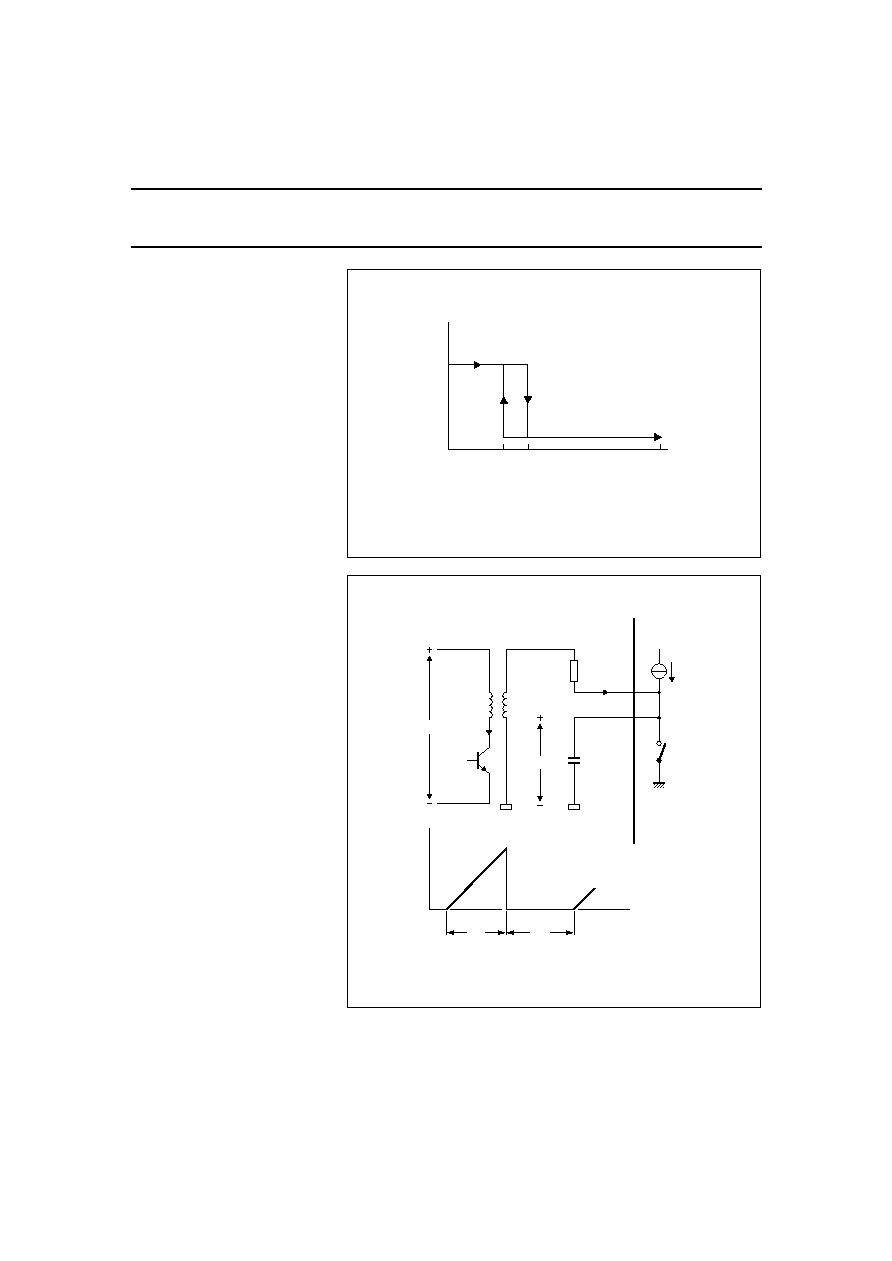
March 1994
6
Philips Semiconductors
Preliminary specification
Control circuit for a Self-Oscillating
Power Supply (SOPS)
TDA8385
Fig.4 Latch initialization as a function of supply voltage V
P
.
5.2
7.5
20
latch
initialization
operation
VP (V)
MCD403
Sawtooth generator (Block II)
C
URRENT SIMULATION
(
SEE FIGS
5
AND
16)
The current of the power supply
switching transistor is detected on the
secondary side by an indirect method
of current sensing.
Information of the collector current (I
c
)
is obtained by integrating the voltage
of an auxiliary winding of the
transformer during transistor on-time
(T
on
). An external capacitor C on pin 5
is charged during T
on
by the current
source I
sim
. The current I
sim
is the
reflection of the current which flows
into pin 12. This current is obtained by
connecting an external resistor R12 to
the auxiliary transformer winding.
During transistor on-time this current
is related to the input voltage V
I
.
During transistor off time (T
off
) the
capacitor C is discharged by switch
sw1. This switch is active during the
total T
off
time. In this way a sawtooth
voltage V
c
is formed across C. This
sawtooth is a measure for the
collector current of the switching
transistor T1.
For the voltage V
c
yields:
(1)
(2)
Where: p = reflection factor;
(2)
(1) gives:
(3)
V
c
I
sim
T
on
◊
C
-------------------------
=
I
sim
p
n
h
n
p
------
◊
V
I
R12
-----------
◊
=
p
I
sim
I
12
---------
0.2
=
=
V
c
p
C
----
n
h
n
p
------
◊
V
I
R12
-----------
◊
T
on
◊
=
Fig.5 Determination of the peak current I
c
.
handbook, full pagewidth
VI
C
R12
I 12
12
5
Isim
L
T1
n p
Ic
n h
Vc
t
MCD404
Vc
Ton
Toff
sw1

March 1994
7
Philips Semiconductors
Preliminary specification
Control circuit for a Self-Oscillating
Power Supply (SOPS)
TDA8385
For `T
on
' yields:
(4)
For the primary current I
c
yields:
(5)
Substitution (4) into (5):
(6)
Equation (6) shows that by limiting the
voltage V
c
the collector peak current
can be limited. The peak current is
limited by means of the clamping
circuit in the transfer character
generator (TCG); see Fig.1
sub-section 4.
The clamping level can be externally
influenced by means of a resistor
on pin 7.
The collector peak current can be
influenced in several ways:
∑
Resistor R12 on pin 12
∑
Capacitor C on pin 5
∑
Capacitor on pin 7
∑
Transfer ratio n
h
/n
p
∑
Inductance L
Before comparing the sawtooth
voltage V
c
with the control voltage V
r
in the pulse width modulator, a
voltage of 100 mV is added to V
c
. In
this way it will be possible for V
r
to
become smaller than V
sim
, which is
important for a stabilized no-load
operation (see Fig.6 area 3).
D
EMAGNETIZATION INPUT
(
PIN
15)
This input prevents the switching
transistor from conducting during
demagnetization of the transformer in
order to prevent the transformer from
going into saturation. The output of
comparator (11) is HIGH as soon as
the voltage of the transformer winding
exceeds 115 mV.
T
on
V
c
C
◊
n
p
◊
R12
◊
p
n
h
◊
V
I
◊
-----------------------------------------------
=
I
c
V
I
L
-----
T
on
◊
=
I
c
C
L
----
1
p
---
◊
n
p
n
h
------
◊
R12
◊
V
c
◊
=
D
ELAY SETTING
(
PIN
6)
The output of sub-section 11 is
extended by the delay circuit of
sub-section 12. The starting
(reference) point of the delay circuit is
the falling edge of the output of
demagnetizing comparator (11) The
delay can be determined externally by
capacitor (C
delay
) on pin 6.
The switch-on moment of the
switching transistor can be
determined by capacitor C
delay
.
A minimum delay time is required to
prevent transistor T1 from switching
during demagnetization of the
transformer because of oscillations
caused by the leakage inductance.
Control part (Block III)
The differential amplifier,
sub-section 3, compares the
feedback voltage (V
fb
) with the
reference voltage V
ref
. The output of
the differential amplifier is available
on pin 11 to allow gain setting. The
differential amplifier is internally
compensated for 0 dB feedback
stability.
The feedback input (pin 9) is also
used as the input for the TCG
(see Fig.6) with which a current
foldback characteristic can be
obtained as shown in Fig.7.
Fig.6 Reference voltage (V
mv
) as a function of feedback voltage (V
fb
).
(1), (2), (3) = V
TCG
.
(4), (5) = V
diff
.
(5)
(4)
(3)
(2)
(1)
MCD405
fb
V
Vmv
VTon(min)
Vclamp
March 1994
8
Philips Semiconductors
Preliminary specification
Control circuit for a Self-Oscillating
Power Supply (SOPS)
TDA8385
Fig.7
Current foldback characteristic; stabilized output voltage (V
O
)
as function of load current (I
O
).
(5)
V
O
I
O
(4)
(3)
(2)
(1)
MCD406
(1), (2), (3) = V
TCG
.
(4), (5) = V
diff
.
The voltage V
Ton(min)
determines the
minimum on-time of the switching
transistor. This voltage can be
determined externally with a resistor
on pin 4. With this resistor the current
foldback characteristic can be
influenced (see dotted line in Figs 6
and 7).
The minimum on-time is of
importance for the following.
∑
Stand-by operation
∑
Starting-up of power supply
∑
Overload and short-circuit
conditions.
The output of the differential amplifier
(V
diff
), the output of the TCG (V
TCG
)
and the voltage V
ss
+ V
Ton(min)
are
compared in a minimum voltage
clamping circuit (see Fig.1
sub-section 6). The output voltage is
equal to the lowest input voltage.
Some relevant characteristics of the
control part are depicted in Fig.8.
Fig.8 Characteristics of the control part.
The voltage V
mv
determines the collector peak current I
c
of transistor T1. The right-hand curve is passed through at start-up. When the feedback voltage
slowly increases from zero, the peak current starts at I
c(min)
and rises along the straight line until I
c(max)
is reached. At a slightly higher feedback voltage
the regulation slope is reached, which is approximately V
ref
.
The plateau of the top between the points x and y has to be kept as small as possible.
The voltage V
diff
decreases with the decreasing load. For good no-load operation the peak current has to be made zero with V
diff
.
Due to the characteristic of the TCG open- and short-circuit feedback loop will result in low peak current.
An additional signal on pin 13 can be supplied which is subtracted from the signal V
mv
. This input can be used for feed forward information.
If no feed forward information is used, pin 13 should be connected to ground.
handbook, full pagewidth
MCD407
Vss +
fb
V
Ic (max)
Ic (min)
Ic
Vmv
x
y
Vref
VTCG
external peak-current
setting (pin 7)
diff
V
mv
V
VTon(min)

March 1994
9
Philips Semiconductors
Preliminary specification
Control circuit for a Self-Oscillating
Power Supply (SOPS)
TDA8385
Pulse width modulator (Block IV)
The pulse width modulator compares
the control voltage V
r
with the
sawtooth voltage V
sim
. If V
sim
>
V
r
output sub-section 8 is HIGH the LED
is switched on and then the switching
transistor is switched off. In this way
the output voltage is controlled.
E
XAMPLE
If the load decreases, V
O
increases
and therefore V
r
decreases. This
causes the LED to start conducting
prematurely, which implies that the
switching transistor is turned off
sooner. The consequence is that the
collector peak current decreases and
hence less energy is stored in the
transformer and V
O
will decrease.
LED control (Block V)
If either output of sub-section 8 or
output of sub-section 16 are HIGH the
LED is conductive. In order to
improve the start-up behaviour of the
power supply, the demagnetization
signal of sub-section 12 will only
activate the LED driver if flip-flop (13)
has previously been set. The set
signal is generated in the following
three ways.
1. Pulse width modulator
(sub-section 8)
2. Comparator (18)
3. V
P(min)
detector
Set signal (2.) and (3.) are added as
extra security to guarantee a
demagnetization pulse in the event of
the switching transistor not having
enough base current. In that situation
e.g. at start-up, no comparator signal,
set signal (3.) is generated by
sub-section 8.
LED driver (Block VI)
The LED driver (pin 2) is blocked if the
supply voltage V
P
is in the
initialization phase (see Fig.4). The
output stage is a push-pull stage,
which can sink 5 mA and source
10 mA.
Slow-start circuit (Block VII)
The slow-start circuit is active at
start-up, over voltage protection or
after an overload (short-circuited),
and stand-by mode. The voltage V
ss
and therefore the voltage V
mv
and the
peak current I
c
slowly increase at
start-up.
By means of sub-section 27 the slow
start voltage V
ss
is clamped to the
voltage V
fb
. If the feedback voltage is
reduced, e.g. as overload, the
slow-start capacitor is discharged to
the level of V
fb
. In this way a slow
start-up is also guaranteed after an
overload, short-circuit situation or
after a stand-by mode. The circuit of
sub-section 27 is not active during an
over voltage protection.
When the supply voltage V
P
is below
the reset-level of 5.2 V
(sub-section 28) the slow-start
capacitor is quickly discharged.
The slow-start input (pin 7) can also
be used for I
c(max)
setting by
connecting a resistor to this pin.
Over voltage protection
(Block VIII)
The operation of the over voltage
protection circuit is, in the event of the
IC being SOPS-supplied, quite
different from when the IC is
externally supplied.
O
PERATION WHEN THE
IC
IS
EXTERNALLY SUPPLIED
When the voltage on pin 8 exceeds
2.5 V the slow-start capacitor is
slowly discharged. During discharge
the LED is permanently conducting.
Discharge is stopped when V
ss
is
below 115 mV. Flip-flop (23) will then
be reset and the circuit is ready again
for a new slow-start procedure.
During an over voltage sub-section 27
is not active so that the output voltage
V
O
cannot influence the slow-start
discharge procedure.
O
PERATION WHEN
IC
IS
SOPS-
SUPPLIED
(
SEE FIGS
9
AND
10)
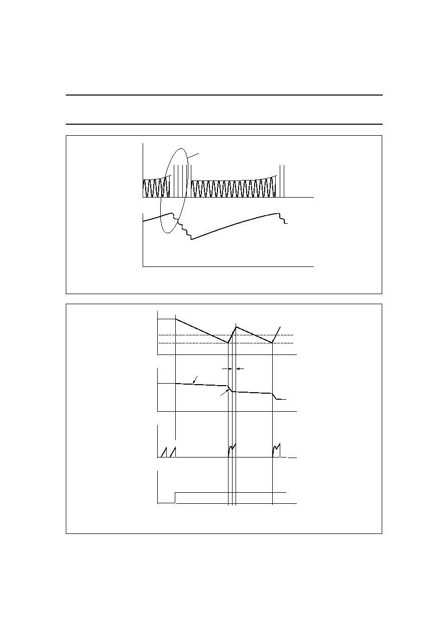
When the voltage on pin 8 exceeds
2.5 V the slow-start capacitor is
slowly discharged. During discharge
of C
ss
the supply capacitor C
P
is also
discharged. Because the capacitors
C
P
and C
ss
have almost the same
value and the supply current I
P
(
15 mA) is much larger than the slow
discharge current (
50
µ
A), the LED
will be switched off by means of the
V
P(min)
detection circuit (5.2 V). At that
moment the switching transistor will
be switched on again until the 7.5 V
level is reached. During this
hysteresis interval the slow-charge
capacitor is quickly discharged. At the
7.5 V level the LED will be switched
on again because flip-flop (23) output
is still HIGH.
The same procedure will be repeated
several times until the slow-start
capacitor reaches the 115 mV reset
level. At that moment the slow-start
procedure is started again.
If there is still an over voltage the
procedure will be repeated.
Figure 10 is a detailed exposure of
Fig.11.
March 1994
10
Philips Semiconductors
Preliminary specification
Control circuit for a Self-Oscillating
Power Supply (SOPS)
TDA8385
handbook, full pagewidth
MCD408
I c
t
V ss
t
(1)
Fig.9 Over voltage protection.
(1) For detail see Fig.10.
Fig.10 Detailed over voltage protection of Fig.9.
0
V P
(V)
t
7.5 V
5.2 V
MCD409
t
Q FF23
t
delay
0
V
ss
(V)
t
slow discharge
quick discharge
I c
t
March 1994
11
Philips Semiconductors
Preliminary specification
Control circuit for a Self-Oscillating
Power Supply (SOPS)
TDA8385
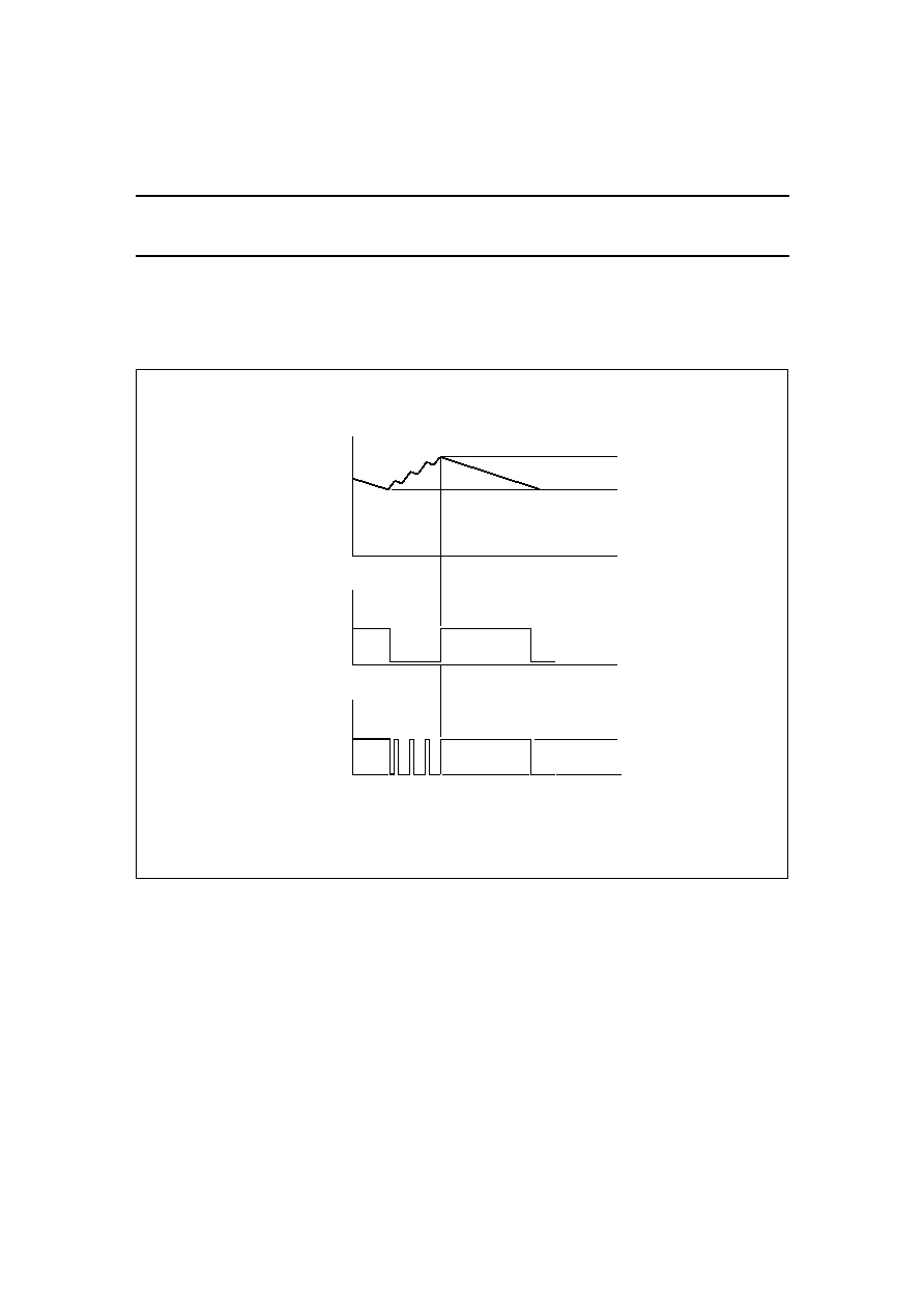
Stand-by circuit (Block IX)
During stand-by operation the voltage V
sb
is supplied from the SOPS via thyristor TH1 (see Fig.16). In the stand-by state,
SOPS operates in a burst mode. When the voltage on pin 10 exceeds 2.5 V the LED driver is permanently activated. The
LED driver is released again if the voltage is below 2 V (see Fig.11).
Fig.11 Stand-by operation; burst mode.
handbook, full pagewidth
MCD410
t
0
output sub-section 25
t
0
t
0
V
sb
(V)
I LED
(mA)
5 mA
2.5 V
2 V
March 1994
12
Philips Semiconductors
Preliminary specification
Control circuit for a Self-Oscillating
Power Supply (SOPS)
TDA8385
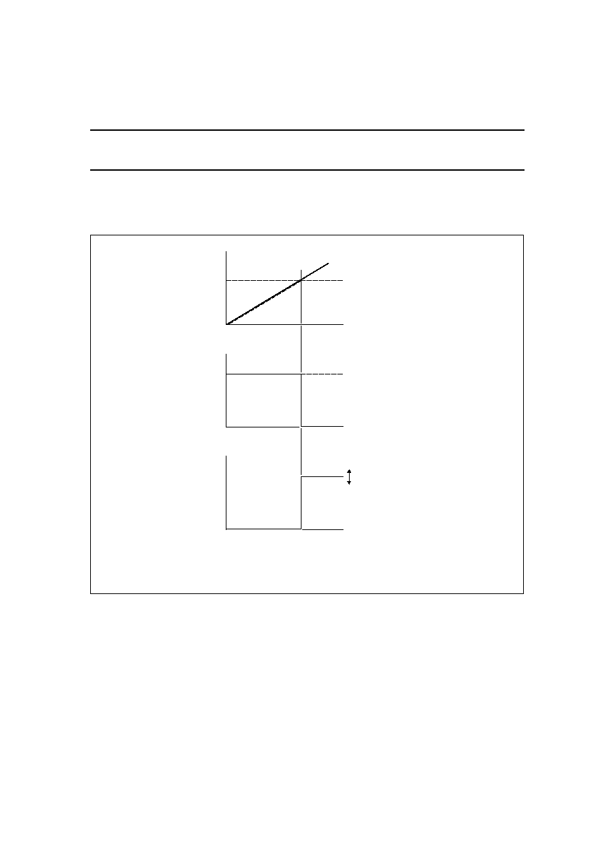
Regulation indicator output (Block X)
Pin 1 can be used to reset the logic circuit in the TV receiver at power on and off. Sub-section 29 has an open-collector
output. The output of this block is LOW during the regulation mode (V
diff
<
V
ts
; see Fig.12).
handbook, full pagewidth
V
2.5
0
t
0
t
V
RIO
0
t
Vfb
Vts
V
diff
VP
V
RIO : open-collector output
MCD411
Fig.12 Regulation indicator output; pin 1.
A desired delay at power-on reset can be made externally.
March 1994
13
Philips Semiconductors
Preliminary specification
Control circuit for a Self-Oscillating
Power Supply (SOPS)
TDA8385
LIMITING VALUES
In accordance with the Absolute Maximum Rating System (IEC 134).
All voltages are measured with respect to ground; positive current flow into the IC; all pins not mentioned in the voltage
list are not allowed to be voltage driven. The voltage ratings are valid provided other ratings are not violated; current
ratings are valid provided the power rating is not violated.
THERMAL RESISTANCE
SYMBOL
PARAMETER
CONDITIONS
MIN.
MAX.
UNIT
Voltages
V
P
supply voltage
pin 2 connected
-
0.5
20
V
pin 2 open-circuit
-
0.5
18
V
V
n
voltage on pins 1, 2, 4, 7, 9 and 13
-
0.5
+18
V
V
3
voltage on pin 3
-
0.5
+6
V
V
8,10
voltage on pins 8 and 10
-
0.5
+3.9
V
V
12
voltage on pin 12
-
0.1
+0.5
V
V
15
voltage on pin 15
-
0.5
+0.5
V
Currents
I
1
current on pin 1
0
2
mA
I
n
current on pins 2, 12 and 15
-
10
+10
mA
I
3
current on pin 3
-
1
0
mA
I
5, 6
current on pins 5 and 6
-
1
+1
mA
I
7
current on pin 7
-
1
+25
mA
I
11
current on pin 11
-
10
+0.5
mA
I
16
current on pin 16
0
20
mA
Temperatures
T
amb
operating ambient temperature
-
25
+70
∞
C
T
stg
storage temperature
-
55
+150
∞
C
Power dissipation
P
tot
total power dissipation
-
500
mW
SYMBOL
PARAMETER
THERMAL RESISTANCE
R
th j-a
from junction to ambient in free air
55 K/W

March 1994
14
Philips Semiconductors
Preliminary specification
Control circuit for a Self-Oscillating
Power Supply (SOPS)
TDA8385
CHARACTERISTICS
V
P
= 15 V; I
3
= 200
µ
A; T
amb
= 25
∞
C; unless otherwise specified.
SYMBOL
PARAMETER
CONDITIONS
MIN.
TYP.
MAX.
UNIT
Supply
V
P
supply voltage (pin 16)
7.9
-
20
V
V
16
supply initialization level
7.1
7.5
7.9
V
V
16(hys)
internal fixed hysteresis
2.5
-
2.55
V
I
16
supply current
active LED output
-
-
20
mA
V
11
supply voltage ripple rejection
see Figs 13 and 14
-
60
-
mV
Reference voltage
V
3
reference voltage at pin 3
0.52
0.55
0.58
V
Error amplifier
V
9
threshold voltage error amplitude
2.4
2.5
2.6
V
I
9
input current feedback input
-
-
0.5
µ
A
I
11
sink current output
V
11
= 80 mV
400
-
-
µ
A
I
11
source current output
V
11
= 2.5 V
500
-
-
µ
A
G
o
open loop gain
-
100
-
dB
B
unity gain bandwidth
-
600
-
kHz
V
9
/
T
temperature coefficient
-
±
300
◊
10
-
6
-
K
-
1
V
5
threshold for switching output
V
diff
= 1.25 V;
V
4
= 2 V; V
13
= 0 V;
V
7
>
V
9
; I
2
= 2 mA
-
V
diff
-
V
os
(1)
-
V
Transfer characteristic generator
I
4
/I
3
current ratio
V
4
= 0.5 V
0.23
0.25
0.27
V
5
threshold for switching output
V
4
= 0.5 V; V
13
= 0 V;
V
7
>
V
9
; I
2
= 2 mA
T
on(min)
V
9
= 0 V
0.4
-
V
os
0.5
-
V
os
0.6
-
V
os
V
V
fb
= 20%
V
9
= 0.4 V
-
0.9
-
V
os
-
V
V
fb
= 50%
V
9
= 1 V
1.4
-
V
os
1.5
-
V
os
1.6
-
V
os
V
V
fb
= 80%
V
9
= 1.6 V
-
2.1
-
V
os
-
V
clamp
V
9
= 2.25 V
2.4
-
V
os
-
2.6
-
V
os
V
t
PLH
response time pulse width
modulation pin 5 to pin 2
LOW-to-HIGH
note 2
-
-
700
ns
t
PHL
response time pulse width
modulation pin 5 to pin 2
HIGH-to-LOW
note 2
-
-
1
µ
s
Feed forward
V
5
threshold for switching output
(V
fo
)
V
4
= 0.5 V; V
13
= 0 V;
V
7
= V
9
= 3 V;
I
2
= 2 mA; V
11
= 1 V
0.6
-
V
os
0.7
-
V
os
0.8
-
V
os
V
I
13
input bias current
V
13
= 0 V
-
-
1
µ
A

March 1994
15
Philips Semiconductors
Preliminary specification
Control circuit for a Self-Oscillating
Power Supply (SOPS)
TDA8385
Slow-start
I
7
/I
3
charge current ratio
V
7
= 0.5 V
0.22
0.24
0.26
I
7
quick discharge current
V
7
= 1 V
20
-
-
mA
V
7
= 100 mV
50
-
-
µ
A
V
7
clamping level
I
7
= 100
µ
A
2.8
3.0
3.2
V
V
5
threshold for switching output
(V
ss
)
V
4
= 0.5 V; V
13
= 0 V;
V
7
= 1 V; I
2
= 2 mA;
V
9
= 2 V
1.4
-
V
os
1.5
-
V
os
1.6
-
V
os
V
Output stage
V
2(sat)
saturation voltage
I
2
= 2 mA
-
-
300
mV
I
2
source current
V
2
= 2 V
operating
4.8
5.3
6.3
mA
initialization phase
-
-
50
µ
A
V
2
open output voltage HIGH
I
2
= 5 mA
12
-
-
V
Current simulation
I
5
/I
12
current ratio
V
5
= 1 V; I
12
= 0.5 mA 0.19
0.2
0.21
V
12
simulation input voltage
I
12
= 0.5 mA
-
-
1.1
V
V
5(sat)
saturation voltage
V
15
= V
6
= 0 V;
I
5
= 1 mA
-
-
300
mV
V
15
= V
6
= 0 V;
I
5
= 200
µ
A
-
-
200
mV
V
threshold for switching output;
voltage difference between pins 5
and 11; offset simulation voltage
(V
os
)
V
4
= 0.5 V; V
13
= 0 V;
V
7
= V
9
= 3 V;
I
2
= 2 mA;
V
11
= 0.5 V
60
100
140
mV
Demagnetization input
t
demLH
delay from pin 15 to pin 5
LOW-to-HIGH
see Fig.15;
pin 6 not connected
-
-
500
ns
t
demHL
delay from pin 15 to pin 5
HIGH-to-LOW
see Fig.15
-
-
1
µ
s
V
15
clamping level
I
15
= 10 mA
positive
-
-
1.2
V
negative
-
-
-
1
V
V
15
demagnetization threshold
voltage
90
115
140
mV
C
15
input capacitance
-
-
10
pF
I
15
input bias current
V
15
= 60 mV
-
-
0.5
µ
A
SYMBOL
PARAMETER
CONDITIONS
MIN.
TYP.
MAX.
UNIT

March 1994
16
Philips Semiconductors
Preliminary specification
Control circuit for a Self-Oscillating
Power Supply (SOPS)
TDA8385
Notes
1. V
os
= V
offset.
2. V
5
pulse = 1 V; V
4
= 0.5 V; V
9
= V
7
= 3 V; V
11
= 0.5 V; V
13
= 0 V; I
2
= 2 mA.
Delay setting
I
6
/I
3
charge current ratio
V
6
= 1 V
1.1
1.2
1.3
I
6
charge current initialization phase V
6
= 1 V; V
16
= 5 V
2
-
-
mA
V
6
clamping level
2.8
-
3.2
V
V
6(sat)
saturation voltage
V
15
= 140 mV
-
50
100
mV
t
dLH
delay from pin 6 to pin 2;
V
6
crossing the 2.5 V level;
LOW-to-HIGH
C
6
= 470 pF;
V
5
= 0 V; I
2
= 2 mA;
V
15
see Fig.15;
excluding capacitive
tolerances
-
-
1.2
µ
s
t/c
delay setting (t = C
6
◊
V/I)
V
6
= 2.5 V;
I
3
= 250
µ
A
-
10
-
ns/pF
Stand-by
V
10H
threshold level HIGH
2.4
2.5
2.6
V
V
10(hys)
hysteresis
450
500
550
mV
t
dLH
delay to output pin 10 to pin 2
LOW-to-HIGH
-
-
1
µ
s
t
dHL
delay to output pin 10 to pin 2
HIGH-to-LOW
-
-
1
µ
s
I
10
input current
V
10
= 2.3 V
-
-
5
µ
A
Over voltage protection
V
8
threshold level
2.4
2.5
2.6
V
t
dLH
delay to output pin 8 to pin 2
LOW-to-HIGH
-
-
1
µ
s
t
dHL
delay to output pin 8 to pin 2
HIGH-to-LOW
-
-
1
µ
s
V
7
reset level
90
-
140
mV
I
7
/I
3
slow discharge current ratio
V
7
= 1 V
0.12
0.23
0.31
I
8
input current
V
8
= 3 V
-
-
1
µ
A
Regulation indicator output
V
1
saturation voltage
I
1
= 1 mA
-
-
300
mV
I
1
leakage current
V
1
= V
16
-
-
1
µ
A
SYMBOL
PARAMETER
CONDITIONS
MIN.
TYP.
MAX.
UNIT
March 1994
17
Philips Semiconductors
Preliminary specification
Control circuit for a Self-Oscillating
Power Supply (SOPS)
TDA8385
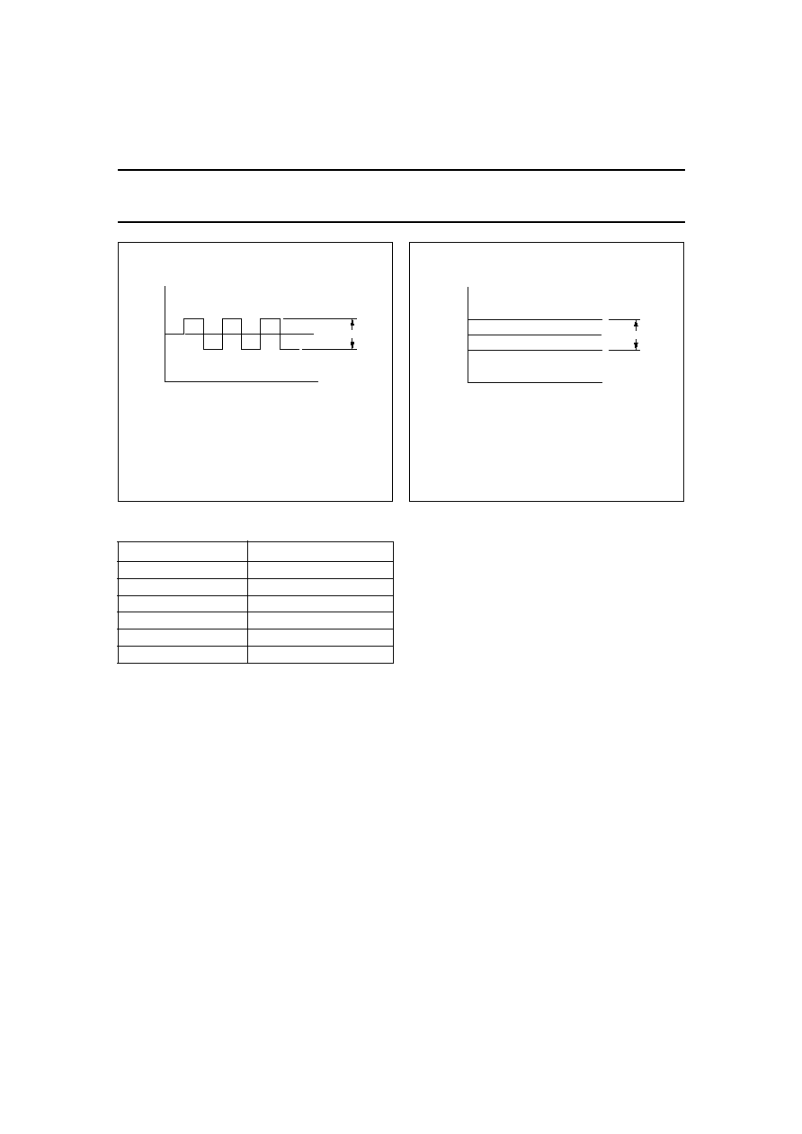
Frequency = 50 kHz.
Slew rate = 0.2
µ
s.
Fig.13 Supply voltage ripple rejection;
V
P
as a function of time.
2 V
15 V
t
V
P
MCD412
Fig.14 Supply voltage ripple rejection;
V
diff
as a function of time.
t
V
diff
MCD413
3 V
~
~
(pin 11)
Frequency = 50 kHz.
Slew rate = 0.2
µ
s.
Table 1 Condition of test circuit used for Figs 13 and 14.
PINS
STATUS
1, 2, 4 to 6, 12, 13
not connected
8 to 10, 14, 15
ground
3
R
ref
= 2.7 k
7
C
ss
= 4.7
µ
F
16
V
P
; see Fig.13
11
V
diff
; see Fig.14
March 1994
18
Philips Semiconductors
Preliminary specification
Control circuit for a Self-Oscillating
Power Supply (SOPS)
TDA8385
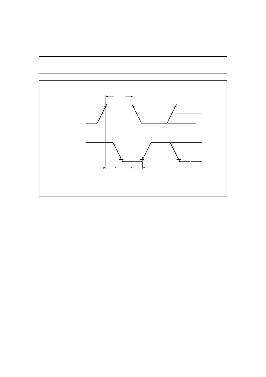
Fig.15 Timing diagram; demagnetization delay time.
handbook, full pagewidth
MCD414
115 mV
90%
10%
t
demLH
demHL
t
~
~ + 0.8 V
0 V
~
~ ≠ 0.8 V
1 V
0 V
peak-current setting input
(pin 5)
demagnetization input
(pin 15)
March 1994
19
Philips Semiconductors
Preliminary specification
Control circuit for a Self-Oscillating
Power Supply (SOPS)
TDA8385
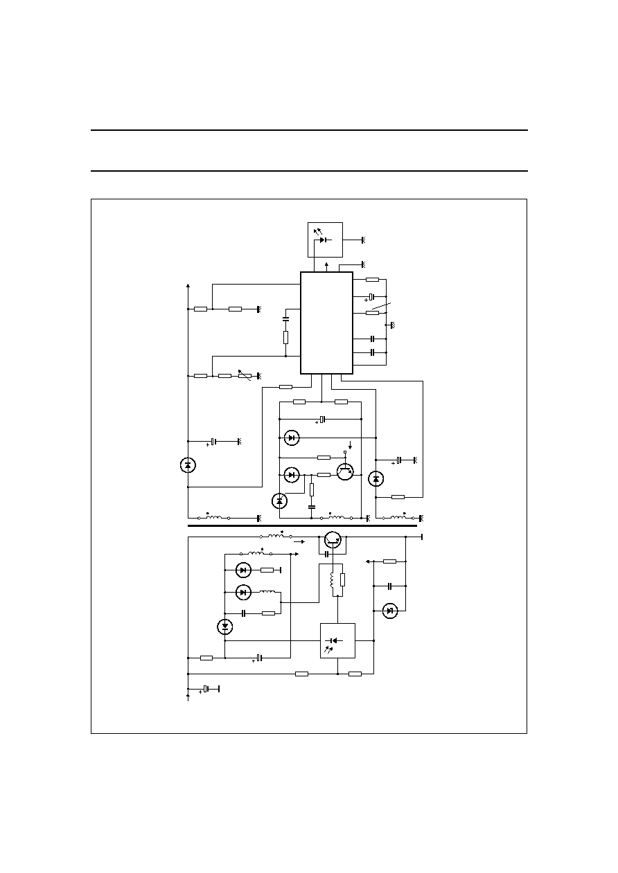
APPLICATION INFORMATION
handbook, full pagewidth
V
O
n
s
V
stab
V
P
C
P
V
f
n
h
1/2 CNR50
n
p
I c
C
o
V
(mains)
I
1/2 CNR50
TDA8385
9
11
8
14
5
6
4
7
3
15
10
16
12
2
1
13
C
ss
R
ref
R
Ton(min)
C
delay
C
R15
R12
RC
TH1
T1
MCD415
A
A
Fig.16 Application circuit of SOPS with stand-by facility.
March 1994
20
Philips Semiconductors
Preliminary specification
Control circuit for a Self-Oscillating
Power Supply (SOPS)
TDA8385
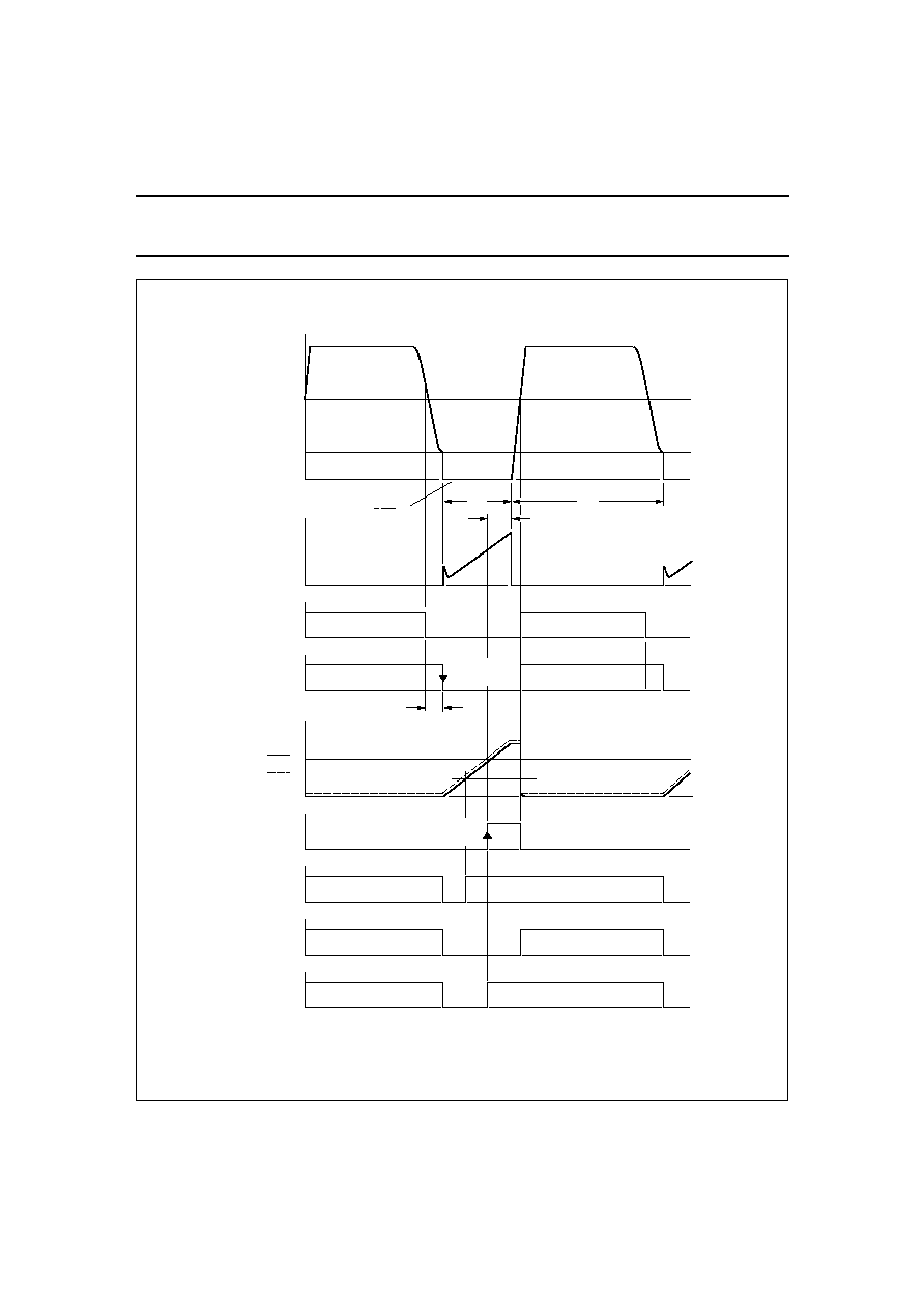
Fig.17 Application timing diagram.
handbook, full pagewidth
output sub-section 11
output sub-section 12
DEMAGNETIZATION
output sub-section 8
COMPARATOR
output sub-section 13
Q
output sub-section 16
DEMAGNETIZATION
output sub-section 14
LED driver
SET
(sub-section 13)
RESET
(sub-section 13)
Toff
Ton
storage time and delay
(SOPS)
delay
Vf
V O
I c
Vsim
Vc
Vr (output sub-section 7)
(output sub-section 10)
Vsim
comparator (18)
level = 1 V
V
I
ns
n p
MCD416
t
March 1994
21
Philips Semiconductors
Preliminary specification
Control circuit for a Self-Oscillating
Power Supply (SOPS)
TDA8385
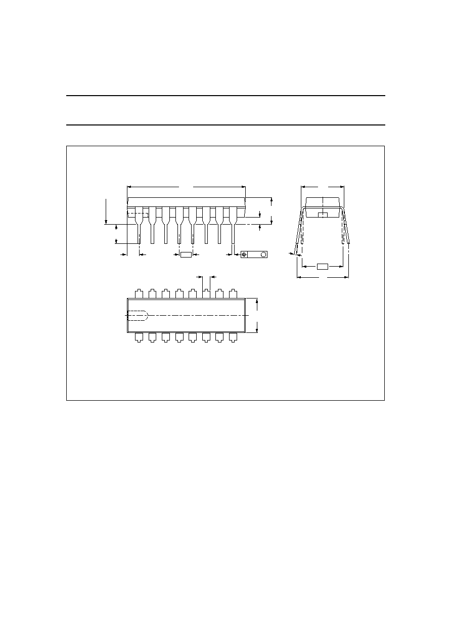
PACKAGE OUTLINE
Fig.18 16-lead dual in-line; plastic with internal heat spreader; opposite bent leads (SOT38WBE).
Dimensions in mm.
8.25
7.80
0.32 max
7.62
9.5
8.3
MSA349
16
1
9
8
1.4 max
6.48
6.14
22.00
21.35
5.1
max
1.2 min
3.9
3.4
seating plane
0.254
M
0.53
max
2.54
(14x)
2.2
max

March 1994
22
Philips Semiconductors
Preliminary specification
Control circuit for a Self-Oscillating
Power Supply (SOPS)
TDA8385
SOLDERING
Plastic dual in-line packages
B
Y DIP OR WAVE
The maximum permissible
temperature of the solder is 260
∞
C;
this temperature must not be in
contact with the joint for more than
5 s. The total contact time of
successive solder waves must not
exceed 5 s.
The device may be mounted up to the
seating plane, but the temperature of
the plastic body must not exceed the
specified storage maximum. If the
printed-circuit board has been
pre-heated, forced cooling may be
necessary immediately after
soldering to keep the temperature
within the permissible limit.
R
EPAIRING SOLDERED JOINTS
Apply a low voltage soldering iron
below the seating plane (or not more
than 2 mm above it). If its temperature
is below 300
∞
C, it must not be in
contact for more than 10 s; if
between 300 and 400
∞
C, for not
more than 5 s.
DEFINITIONS
LIFE SUPPORT APPLICATIONS
These products are not designed for use in life support appliances, devices, or systems where malfunction of these
products can reasonably be expected to result in personal injury. Philips customers using or selling these products for
use in such applications do so at their own risk and agree to fully indemnify Philips for any damages resulting from such
improper use or sale.
Data sheet status
Objective specification
This data sheet contains target or goal specifications for product development.
Preliminary specification
This data sheet contains preliminary data; supplementary data may be published later.
Product specification
This data sheet contains final product specifications.
Limiting values
Limiting values given are in accordance with the Absolute Maximum Rating System (IEC 134). Stress above one or
more of the limiting values may cause permanent damage to the device. These are stress ratings only and operation
of the device at these or at any other conditions above those given in the Characteristics sections of the specification
is not implied. Exposure to limiting values for extended periods may affect device reliability.
Application information
Where application information is given, it is advisory and does not form part of the specification.