 | –≠–ª–µ–∫—Ç—Ä–æ–Ω–Ω—ã–π –∫–æ–º–ø–æ–Ω–µ–Ω—Ç: TDA8442 | –°–∫–∞—á–∞—Ç—å:  PDF PDF  ZIP ZIP |
Document Outline
- GENERAL DESCRIPTION
- PACKAGE OUTLINE
- QUICK REFERENCE DATA
- PINNING
- FUNCTIONAL DESCRIPTION
- OPERATION
- Write
- Control
- POD bit P1
- POD bit P2/P2N
- DAX bits AX5 to AX0
- RATINGS
- CHARACTERISTICS
- I 2 C-BUS TIMING
- PACKAGE OUTLINE
- SOLDERING
- DEFINITIONS
- LIFE SUPPORT APPLICATIONS
- PURCHASE OF PHILIPS I 2 C COMPONENTS

DATA SHEET
Product specification
File under Integrated Circuits, IC01
March 1991
INTEGRATED CIRCUITS
TDA8442
I
2
C-bus interface for colour
decoders

March 1991
2
Philips Semiconductors
Product specification
I
2
C-bus interface for colour decoders
TDA8442
GENERAL DESCRIPTION
The TDA8442 provides control of four analogue functions
and has one high-current and two switching outputs.
Control of the IC is performed via the two-line, bidirectional
I
2
C-bus.
Features
∑
Four analogue control outputs
∑
One high-current output port (npn open emitter)
∑
Two switching output ports (npn collector with internal
pull-up resistor)
∑
I
2
C-bus slave receiver
∑
Power-down reset.
PACKAGE OUTLINE
16-lead DIL; plastic (SOT38); SOT38-1; 1996 July 23.
QUICK REFERENCE DATA
PARAMETER
CONDITIONS
SYMBOL
MIN.
TYP.
MAX
UNIT
Supply voltage (pin 9)
V
P
10.8
12.0
13.2
V
Supply current
no outputs loaded
I
P
8
13
18
mA
Total power dissipation
no outputs loaded
P
tot
-
-
1
W
Operating ambient
temperature range
T
amb
-
20
-
+
70
∞
C
Fig.1 Block diagram.
March 1991
3
Philips Semiconductors
Product specification
I
2
C-bus interface for colour decoders
TDA8442
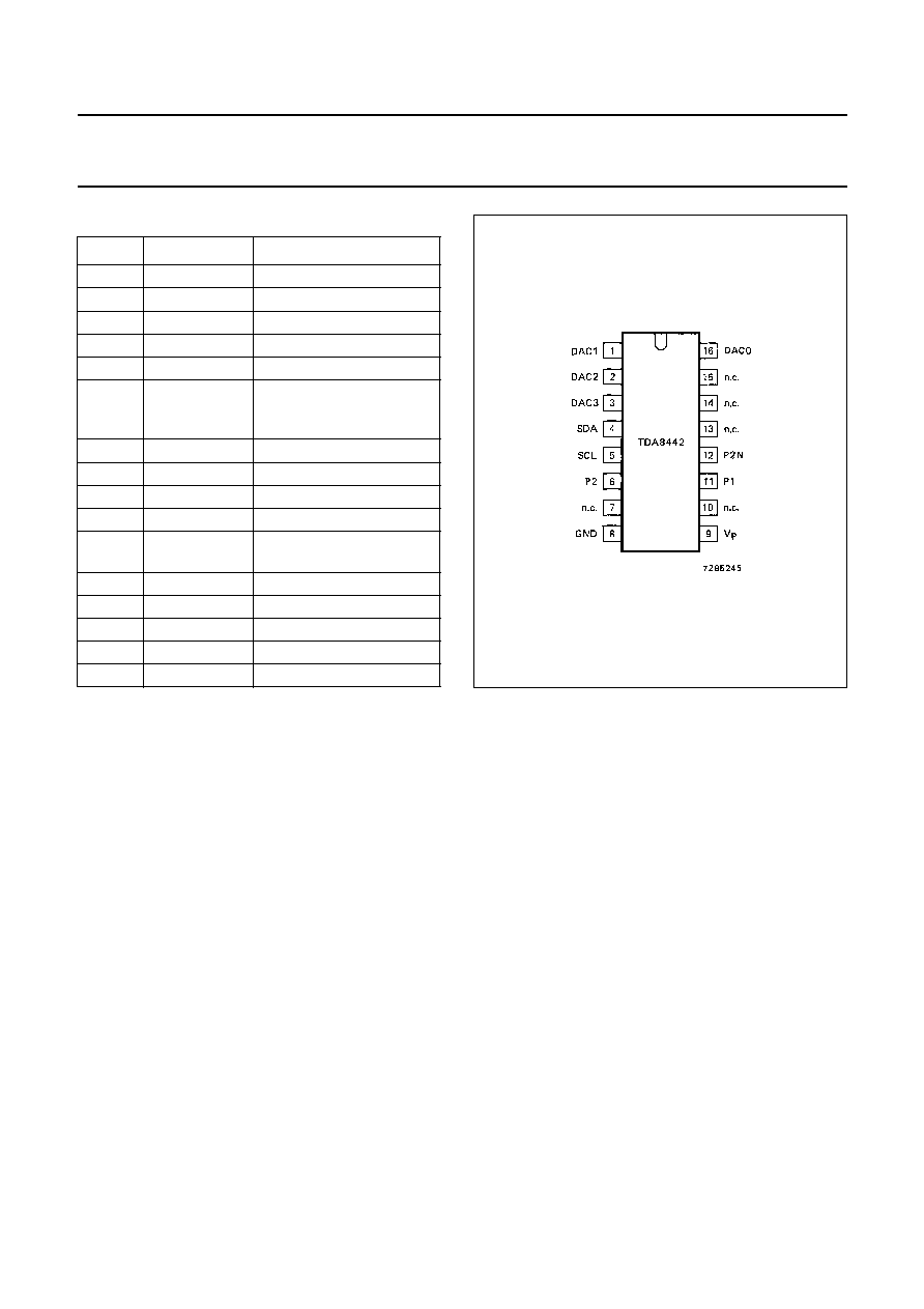
PINNING
PIN
SYMBOL
DESCRIPTION
1
DAC1
analogue output 1
2
DAC2
analogue output 2
3
DAC3
analogue output 3
4
SDA
serial data line; I
2
C-bus
5
SCL
serial clock line; I
2
C-bus
6
P2
Port 2 npn collector output
with internal pull-up
resistor
7
n.c.
not connected
8
GND
supply return (ground)
9
V
P
positive supply voltage
10
n.c.
not connected
11
P1
Port 1 open npn emitter
output
12
P2N
inverted P2 output
13
n.c.
not connected
14
n.c.
not connected
15
n.c.
not connected
16
DAC0
analogue output 0
Fig.2 Pinning diagram
FUNCTIONAL DESCRIPTION
Control
Analogue control is facilitated by four 6-bit digital-to-analogue converters (DAC0 to DAC3).
The values of the output voltages from the DACs are set via the I
2
C-bus.
The high-current output port (P1) is suitable for switching between internal and external RGB signals.
It is an open npn emitter output capable of sourcing 14 mA (min.).
The two output ports (P2 and P2N) can be used for NTSC/PAL switching. These are npn collector outputs with internal
pull-up resistors of 10 k
(typ.). Both outputs are capable of sinking up to 2 mA with a voltage drop of less than 400 mV.
If one output is switched on (LOW), the other output is switched off, and vice versa.
Reset
The power-down-reset mode occurs whenever the positive supply voltage falls below 8.5 V (typ.) and resets all registers
to a defined state.

March 1991
4
Philips Semiconductors
Product specification
I
2
C-bus interface for colour decoders
TDA8442
OPERATION
Write
The TDA8442 is controlled via the I
2
C-bus (specifications for the I
2
C-bus will be supplied on request).
Programming of the TDA8442 is performed using the format shown in Fig.3.
Acknowledge (A) is generated by the TDA8442 only when a valid address is received and the device is not in the
power-down-reset mode (V
P
> 8.5 V (typ.)).
Control
Control is implemented by the instruction bytes POD (port output data) and DACX (digital-to-analogue converter control)
together with the corresponding data/control bytes (see Fig.4).
POD bit P1
If a logic 1 is programmed, the P1 output is switched on. If a logic 0 is programmed or after a power-down-reset, the P1
output is switched off (high-impedance state).
POD bit P2/P2N
If a logic 1 is programmed, the P2 output is switched off and the P2N output is switched on (LOW). If a logic 0 is
programmed or after a power-down-reset, the P2 output is switched on (LOW) and the P2N output is switched off.
DAX bits AX5 to AX0
The digital-to-analogue converter selected corresponds to the decimal equivalent of the two bits X1 and X0. The output
voltage of the selected DAC is programmed using bits AX5 to AX0, the lowest value being with all data AX5 to AX0 at
logic 0 or when power-down-reset has been activated.
Fig.3 TDA8442 programming format.
Fig.4 Control porgramming.
March 1991
5
Philips Semiconductors
Product specification
I
2
C-bus interface for colour decoders
TDA8442
RATINGS
Limiting values in accordance with the Absolute Maximum System (IEC 134)
Note
1. Pin voltage may exceed V
P
if the current in that pin is limited to 10 mA.
CHARACTERISTICS
V
P
= 12 V; T
amb
=
+
25
∞
C; unless otherwise specified
PARAMETER
SYMBOL
MIN.
MAX.
UNIT
Supply voltage range (pin 9)
V
P
-
0.3
+
13.2
V
Input/output voltage ranges
pin 4
V
SDA
-
0.3
+
13.2
V
pin 5
V
SCL
-
0.3
+
13.2
V
pin 6
V
P2
-
0.3
V
P
; note 1
V
pin 11
V
P1
-
0.3
V
P
; note 1
V
pin 12
V
P2N
-
0.3
V
P
; note 1
V
pin 1 to 3 and pin 16
V
DAX
-
0.3
V
P
; note 1
V
Total power dissipation
P
tot
-
1
W
Operating ambient temperature range
T
amb
-
20
+
70
∞
C
Storage temperature range
T
stg
-
55
+
150
∞
C
PARAMETER
CONDITIONS
SYMBOL
MIN.
TYP.
MAX.
UNIT
Supplies
Supply voltage (pin 9)
V
P
10.8
12.0
13.2
V
Supply current (pin 9)
no outputs loaded
I
P
8
13
18
mA
I
2
C-bus inputs
SDA (pin 4); SCL (pin 5)
Input voltage HIGH
note 1
V
IH
3.0
-
V
P
-
1
V
Input voltage LOW
V
IL
-
0.3
-
1.5
V
Input current HIGH
note 1
I
IH
-
-
10
µ
A
Input current LOW
note 1
I
IL
-
-
10
µ
A
I
2
C-bus output
SDA (pin 4)
open collector
Output voltage LOW
I
OL
= 3.0 mA
V
OL
-
-
0.4
V
Maximum output sink current
I
OL
3
5
-
mA