
DATA SHEET
Preliminary specification
File under Integrated Circuits, IC01
July 1994
INTEGRATED CIRCUITS
TDA8561Q
2 x 24 W BTL or 4 x 12 W
single-ended car radio power
amplifier

July 1994
2
Philips Semiconductors
Preliminary specification
2 x 24 W BTL or 4 x 12 W single-ended
car radio power amplifier
TDA8561Q
FEATURES
∑
Requires very few external components
∑
High output power
∑
Flexibility in use - Quad single-ended or stereo BTL
∑
Low output offset voltage
∑
Fixed gain
∑
Diagnostic facility (distortion, short-circuit and
temperature detection)
∑
Good ripple rejection
∑
Mode select switch (operating, mute and stand-by)
∑
Load dump protection
∑
AC and DC short-circuit safe to ground and to V
P
∑
Low power dissipation in any short-circuit condition
∑
Thermally protected
∑
Reverse polarity safe
∑
Electrostatic discharge protection
∑
No switch-on/switch-off plop
∑
Flexible leads
∑
Low thermal resistance
∑
Identical inputs (inverting and non-inverting).
GENERAL DESCRIPTION
The TDA8561Q is an integrated class-B output amplifier in
a 17-lead single-in-line (SIL) power package. It contains 4
x 12 W single-ended or 2 x 24 W bridge amplifiers.
The device is primarily developed for car radio
applications.
QUICK REFERENCE DATA
SYMBOL
PARAMETER
CONDITIONS
MIN.
TYP.
MAX.
UNIT
V
P
positive operating supply voltage
6
14.4
18
V
I
ORM
repetitive peak output current
-
-
4
A
I
P
total quiescent current
-
80
-
mA
I
sb
stand-by current
-
0.1
100
µ
A
Stereo BTL application
P
O
output power
4
; THD = 10%
-
24
-
W
RR
supply voltage ripple rejection
48
-
-
dB
V
no
noise output voltage
R
s
= 0
-
70
-
µ
V
Z
I
input impedance
25
-
-
k
V
O
|
DC output offset voltage
-
-
150
mV
Quad single-ended application
P
O
output power
THD = 10%
4
-
7
-
W
2
-
12
-
W
RR
supply voltage ripple rejection
48
-
-
dB
V
no
noise output voltage
R
s
= 0
-
50
-
µ
V
Z
I
input impedance
50
-
-
k

July 1994
3
Philips Semiconductors
Preliminary specification
2 x 24 W BTL or 4 x 12 W single-ended car
radio power amplifier
TDA8561Q
ORDERING INFORMATION
Note
1. SOT243-1; 1996 August 30.
EXTENDED TYPE NUMBER
PACKAGE
PINS
PIN POSITION
MATERIAL
CODE
TDA8561Q
17
DBS
plastic
SOT243R
(1)

July 1994
4
Philips Semiconductors
Preliminary specification
2 x 24 W BTL or 4 x 12 W single-ended car
radio power amplifier
TDA8561Q
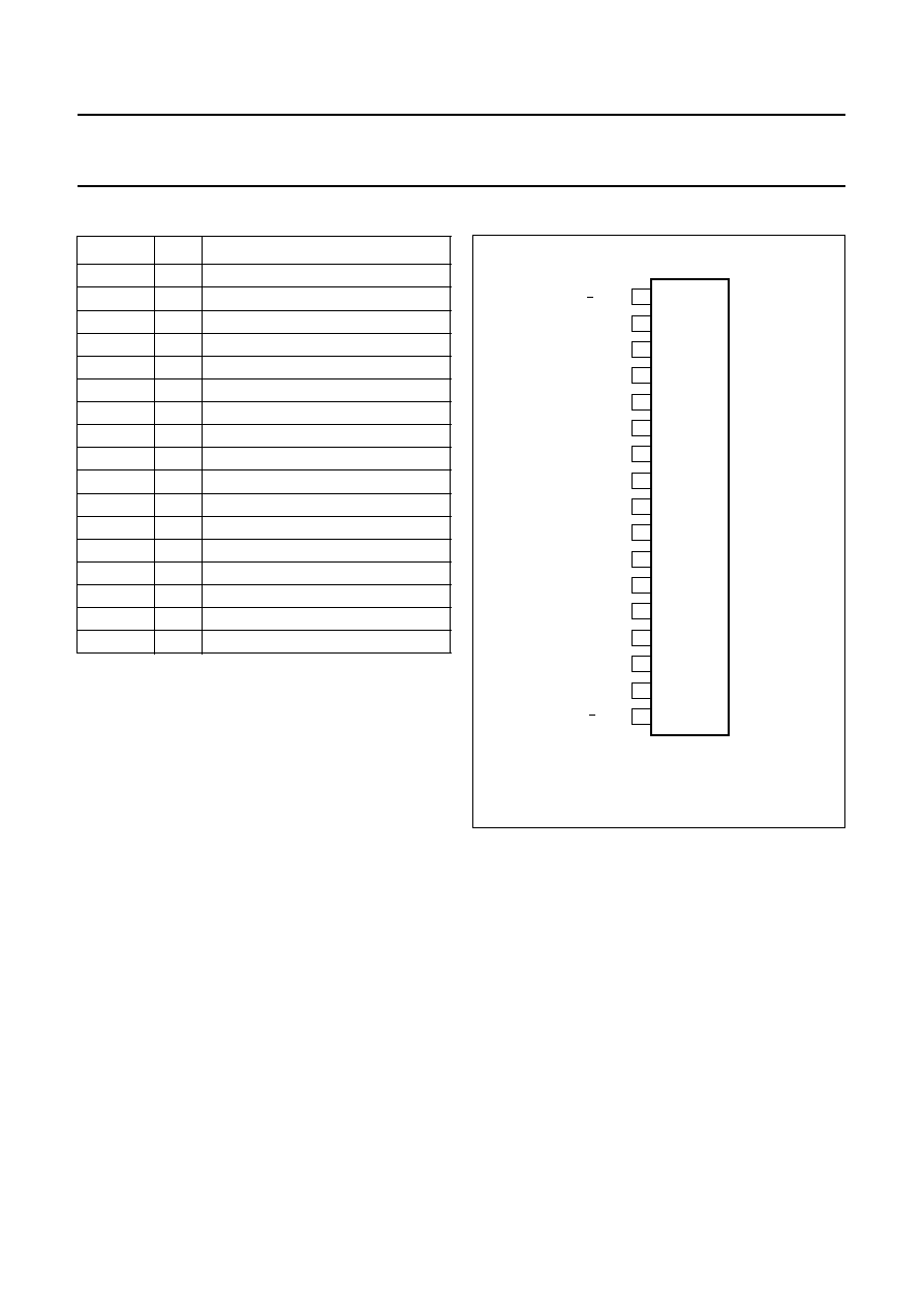
Fig.1 Block diagram.
mode
select
switch
MEA858 - 1
output 1
15 k
15 k
x1
VA
stand-by
switch
VP
mute
switch
stand-by
reference
voltage
5
13
VP1
VP2
18 k
2
k
mute switch
VA
Cm
power stage
18 k
mute switch
VA
Cm
power stage
6
8
14
18 k
mute switch
VA
Cm
power stage
18 k
mute switch
VA
Cm
power stage
12
10
2
7
11
ground
(signal)
GND1
GND2
power ground (substrate)
output 4
output 3
output 2
non-inverting
input 1
non-inverting
input 4
17
1
TDA8561Q
mute
reference
voltage
input
reference
voltage
2
k
60
k
60
k
inverting
input 2
3
PROTECTIONS
thermal
short-circuit
diagnostic
output
16
4
supply voltage
ripple rejection
inverting
input 3
15
2
k
60
k
2
k
60
k
9
not connected
July 1994
5
Philips Semiconductors
Preliminary specification
2 x 24 W BTL or 4 x 12 W single-ended car
radio power amplifier
TDA8561Q
PINNING
SYMBOL
PIN
DESCRIPTION
-
INV 1
1
non-inverting input 1
GND(S)
2
signal ground
INV 2
3
inverting input 2
RR
4
supply voltage ripple rejection
V
P1
5
supply voltage
OUT 1
6
output 1
GND1
7
power ground 1
OUT 2
8
output 2
n.c.
9
not connected
OUT 3
10
output 3
GND2
11
power ground 2
OUT 4
12
output 4
V
P2
13
supply voltage
MODE
14
mode select switch input
INV 3
15
inverting input 3
V
DIAG
16
diagnostic output
-
INV 4
17
non-inverting input 4
Fig.2 Pin configuration.
1
2
3
4
5
6
7
8
9
10
11
12
13
14
15
16
17
TDA8561Q
INV 1
GND(S)
INV 2
RR
OUT 1
GND1
OUTP 2
n.c.
OUT 3
GND2
OUTP 4
V
MODE
INV 3
DIAG
INV 4
P2
V P1
MEA859 - 1
V
FUNCTIONAL DESCRIPTION
The TDA8561Q contains four identical amplifiers and can
be used for single-ended or bridge applications. The gain
of each amplifier is fixed at 20 dB (26 dB in BTL).
Special features of the device are:
Mode select switch (pin 14)
∑
low stand-by current (< 100
µ
A)
∑
low switching current (low cost supply switch)
∑
mute facility
To avoid switch-on plops, it is advised to keep the amplifier
in the mute mode during
100 ms (charging of the input
capacitors at pin 1, 3, 15 and pin 17).
This can be achieved by:
∑
microprocessor control
∑
external timing circuit (see Fig.11)
Diagnostic output (pin 16)
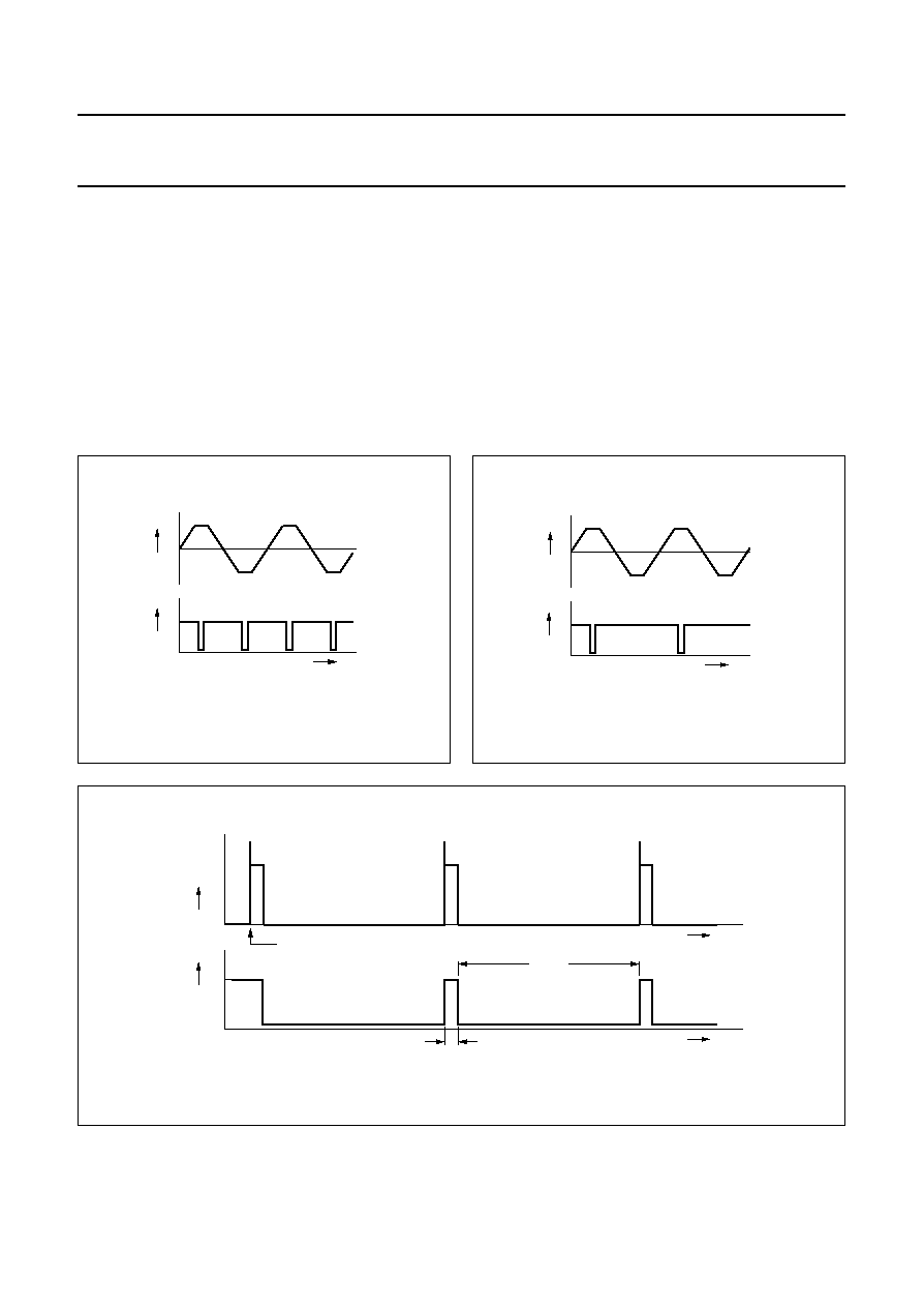
DYNAMIC DISTORTION DETECTOR
(DDD)
At the onset of clipping of one or more output stages, the
dynamic distortion detector becomes active and pin 16
goes low. This information can be used to drive a sound
processor or DC volume control to attenuate the input
signal and thus limit the distortion. The output level of pin
16 is independent of the number of channels that are
clipping (see Fig.3 and Fig.4).
July 1994
6
Philips Semiconductors
Preliminary specification
2 x 24 W BTL or 4 x 12 W single-ended car
radio power amplifier
TDA8561Q
SHORT
-
CIRCUIT PROTECTION
When a short-circuit occurs at one or more outputs to ground or to the supply voltage, the output stages are switched off
until the short-circuit is removed and the device is switched on again, with a delay of approximately 20 ms, after removal
of the short-circuit. During this short-circuit condition, pin 16 is continuously low.
When a short-circuit across the load of one or both channels occurs the output stages are switched off during
approximately 20 ms. After that time it is checked during approximately 50
µ
s to see whether the short-circuit is still
present. Due to this duty cycle of 50
µ
s/20 ms the average current consumption during this short-circuit condition is very
low (approximately 40 mA).
During this short-circuit condition, pin 16 is low for 20 ms and high for 50
µ
s (see Fig.5).
The power dissipation in any short-circuit condition is very low.
Fig.3
Distortion detector waveform; BTL
application.
andbook, halfpage
V
0
VP
VO
0
t
MGA705
16
Fig.4
Distortion detector waveform; single-ended
application.
ndbook, halfpage
0
VP
VO
t
0
MGA706
V16
Fig.5 Short-circuit waveform.
handbook, full pagewidth
MGA707
short-circuit over the load
20 ms
50
µ
s
t
t
VP
current
in
output
stage
V15

July 1994
7
Philips Semiconductors
Preliminary specification
2 x 24 W BTL or 4 x 12 W single-ended car
radio power amplifier
TDA8561Q
TEMPERATURE DETECTION
When the virtual junction temperature T
vj
reaches 150
∞
C, pin 16 will be active LOW.
OPEN COLLECTOR OUTPUT
Pin 16 is an open collector output, which allows pin 16 of more devices being tied together.
LIMITING VALUES
In accordance with the absolute maximum system (IEC 134).
THERMAL RESISTANCE
In accordance with IEC 747-1.
SYMBOL
PARAMETER
CONDITIONS
MIN.
MAX.
UNIT
v
p
positive supply voltage
operating
-
18
V
non-operating
-
30
V
load dump protection
during 50 ms; t
r
2.5 ms
-
45
V
I
OSM
non-repetitive peak output current
-
6
A
I
ORM
repetitive peak output current
-
4
A
T
stg
storage temperature
-
55
+150
∞
C
T
amb
operating ambient temperature
-
40
+85
∞
C
T
vj
virtual junction temperature
-
150
∞
C
V
psc
AC and DC short-circuit safe voltage
-
18
V
V
pr
reverse polarity
-
6
V
P
tot
total power dissipation
-
60
W
SYMBOL
PARAMETER
THERMAL RESISTANCE
R
th j-a
from junction to ambient in free air
40 K/W
R
th j-c
from junction to case (see Fig.6 and Fig.7)
1.3 K/W
July 1994
8
Philips Semiconductors
Preliminary specification
2 x 24 W BTL or 4 x 12 W single-ended car
radio power amplifier
TDA8561Q
Fig.6
Equivalent thermal resistance network;
BTL application.
handbook, halfpage
2.2 K/W
0.2 K/W
2.2 K/W
virtual junction
output 1
output 2
case
MEA861 - 1
Fig.7
Equivalent thermal resistance network;
single-ended application.
handbook, halfpage
3.0 K/W
0.7 K/W
3.0 K/W
virtual junction
output 1
output 2
case
3.0 K/W
0.7 K/W
3.0 K/W
output 3
output 4
MEA860 - 2
0.2 K/W

July 1994
9
Philips Semiconductors
Preliminary specification
2 x 24 W BTL or 4 x 12 W single-ended car
radio power amplifier
TDA8561Q
DC CHARACTERISTICS
V
P
= 14.4 V; T
amb
= 25
∞
C; measured in Fig.8; unless otherwise specified.
SYMBOL
PARAMETER
CONDITIONS
MIN.
TYP.
MAX.
UNIT
Supply
V
P
positive supply voltage
note 1
6
14.4
18
V
I
P
quiescent current
-
80
160
mA
V
O
DC output voltage
note 2
-
6.9
-
V
V
O
DC output offset voltage
-
-
150
mV
Mode select switch
V
on
switch-on voltage level
8.5
-
-
V
MUTE CONDITION
V
mute
mute voltage
3.3
-
6.4
V
V
O
output voltage in mute position
V
Imax
= 1 V; f = 1 kHz
-
-
2
mV
V
O
DC output offset voltage (between
pins 6-8 and 10-12)
-
-
150
mV
STAND
-
BY CONDITION
V
sb
stand-by voltage
0
-
2
V
I
sb
stand-by current
-
-
100
µ
A
I
sw
switch-on current
-
12
40
µ
A
Diagnostic output (pin 16)
V
DIAG
diagnostic output voltage
any short-circuit or clipping
-
-
0.6
V

July 1994
10
Philips Semiconductors
Preliminary specification
2 x 24 W BTL or 4 x 12 W single-ended car
radio power amplifier
TDA8561Q
AC CHARACTERISTICS
V
P
= 14.4 V; R
L
= 4
; f = 1 kHz; T
amb
= 25
∞
C; unless otherwise specified.
SYMBOL
PARAMETER
CONDITIONS
MIN.
TYP.
MAX.
UNIT
Stereo BTL application (measured in Fig.8)
P
O
output power
note 7
THD = 0.5%
15
19
-
W
THD = 10%
20
24
-
W
THD
total harmonic distortion
P
O
= 1 W
-
0.1
-
%
P
O
output power
V
P
= 13.2 V
THD = 0.5%
-
16
-
W
THD = 10%
-
20
-
W
B
power bandwidth
THD = 0.5%;
-
20 to
-
Hz
P
O
=
-
1 dB; with respect to
15 W
15000
f
l
low frequency roll-off
at
-
1 dB; note 3
-
45
-
Hz
f
h
high frequency roll-off
at
-
1 dB
20
-
-
kHz
G
v
closed loop voltage gain
25
26
27
dB
RR
supply voltage ripple rejection
note 4
on
48
-
-
dB
mute
48
-
-
dB
stand-by
80
-
-
dB
Z
I
input impedance
25
30
38
k
V
no
noise output voltage
on
R
s
= 0
; note 5
-
70
-
µ
V
on
R
s
= 10 k
; note 5
-
100
200
µ
V
mute
notes 5 and 6
-
60
-
µ
V
channel separation
R
s
= 10 k
40
-
-
dB
G
v
channel unbalance
-
-
1
dB
DYNAMIC DISTORTION DETECTOR
THD
total harmonic distortion
V
16
0.6 V; no short-circuit
-
10
-
%
Quad single-ended application (measured in Fig.9)
P
O
output power
note 7
THD = 0.5%
4
5
-
W
THD = 10%
5.5
7
-
W
THD
total harmonic distortion
P
O
= 1 W
-
0.1
-
%
P
O
output power
R
L
= 2
; note 7
THD = 0.5%
7.5
10
-
W
THD = 10%
10
12
-
W
f
l
low frequency roll-off
at
-
3 dB; note 3
-
45
-
Hz
f
h
high frequency roll-off
at
-
1 dB
20
-
-
kHz
G
v
closed loop voltage gain
19
20
21
dB

July 1994
11
Philips Semiconductors
Preliminary specification
2 x 24 W BTL or 4 x 12 W single-ended car
radio power amplifier
TDA8561Q
Notes
1. The circuit is DC adjusted at V
P
= 6 to 18 V and AC operating at V
P
= 8.5 to 18 V.
2. At 18 V < V
P
< 30 V the DC output voltage
V
P
/2.
3. Frequency response externally fixed.
4. Ripple rejection measured at the output with a source impedance of 0
, maximum ripple amplitude of 2 V (p-p) and
at a frequency of between 100 Hz and 10 kHz.
5. Noise measured in a bandwidth of 20 Hz to 20 kHz.
6. Noise output voltage independent of R
s
(V
i
= 0 V).
7. Output power is measured directly at the output pins of the IC.
RR
supply voltage ripple rejection
note 4
on
48
-
-
dB
mute
48
-
-
dB
stand-by
80
-
-
dB
Z
I
input impedance
50
60
75
k
V
no
noise output voltage
on
R
s
= 0
; note 5
-
50
-
µ
V
on
R
s
= 10 k
; note 5
-
70
100
µ
V
mute
notes 5 and 6
-
50
-
µ
V
channel separation
R
s
= 10 k
40
-
-
dB
G
v
channel unbalance
-
-
1
dB
DYNAMIC DISTORTION DETECTOR
THD
total harmonic distortion
V
16
0.6 V; no short-circuit
-
10
-
%
SYMBOL
PARAMETER
CONDITIONS
MIN.
TYP.
MAX.
UNIT

July 1994
12
Philips Semiconductors
Preliminary specification
2 x 24 W BTL or 4 x 12 W single-ended car
radio power amplifier
TDA8561Q
TEST/APPLICATION INFORMATION
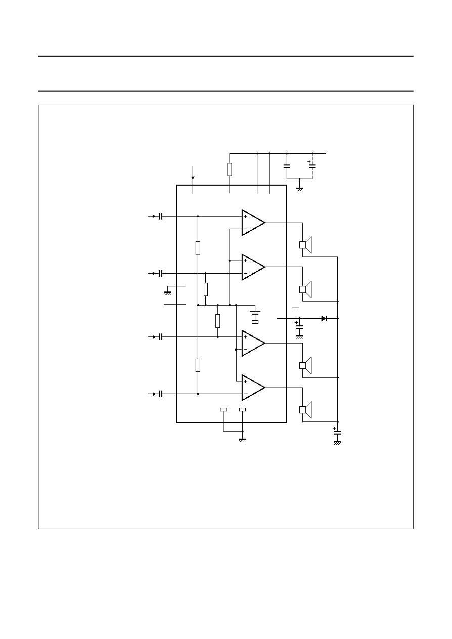
Fig.8 Stereo BTL application diagram.
handbook, full pagewidth
MEA862 - 2
100
nF
16
5
13
220 nF
1
6
8
7
11
VP
TDA8561Q
TDA8564Q
2200
µ
F
60
k
2
ground (signal)
10
k
14
9
not connected
3
inverting input 2
60
k
60
k
reference
voltage
220 nF
17
12
60
k
non-inverting
input 4
4
15
10
power ground (substrate)
non- inverting
input 1
supply voltage
ripple rejection
inverting input 3
diagnostic
mode
switch

July 1994
13
Philips Semiconductors
Preliminary specification
2 x 24 W BTL or 4 x 12 W single-ended car
radio power amplifier
TDA8561Q
Fig.9 Quad single-ended application diagram 1.
handbook, full pagewidth
MEA863 - 2
100
nF
16
5
13
220 nF
1
6
8
7
11
VP
TDA8561Q
TDA8564Q
2200
µ
F
60
k
2
ground (signal)
10
k
14
9
not connected
3
inverting
input 2
60
k
60
k
reference
voltage
220 nF
17
12
60
k
non-inverting
input 4
4
15
10
power ground (substrate)
non- inverting
input 1
supply voltage
ripple rejection
inverting
input 3
220 nF
1/2Vp
1000
µ
F
220 nF
1000
µ
F
1000
µ
F
1000
µ
F
mode
switch
July 1994
14
Philips Semiconductors
Preliminary specification
2 x 24 W BTL or 4 x 12 W single-ended car
radio power amplifier
TDA8561Q
Fig.10 Quad single-ended application diagram 2.
(1) When short-circuiting the single-ended capacitor, the dissipation will be reduced due to diode D1.
handbook, full pagewidth
MEA864 - 2
100
nF
16
5
13
220 nF
1
6
8
7
11
VP
VP
TDA8561Q
TDA8564Q
2200
µ
F
60
k
2
ground (signal)
10
k
14
4
not connected
3
inverting
input 2
60
k
60
k
reference
voltage
220 nF
17
12
60
k
non-inverting
input 4
9
15
10
power ground (substrate)
non- inverting
input 1
inverting
input 3
220 nF
220 nF
2200
µ
F
2
D1
100
µ
F
mode
switch

July 1994
15
Philips Semiconductors
Preliminary specification
2 x 24 W BTL or 4 x 12 W single-ended car
radio power amplifier
TDA8561Q
Fig.11 Mode select switch circuitry.
handbook, halfpage
100 k
MGA708
47
µ
F
10 k
10 k
mode
select
switch
VP
Mode select switch
To avoid switch-on plops, it is advised to keep the amplifier
in the mute mode during > 100 ms (charging of the input
capacitors at pins 1, 3, 15 and 17.
The circuit in Fig.11 slowly ramps up the voltage at the
mode select switch pin when switching on and results in
fast muting when switching off.
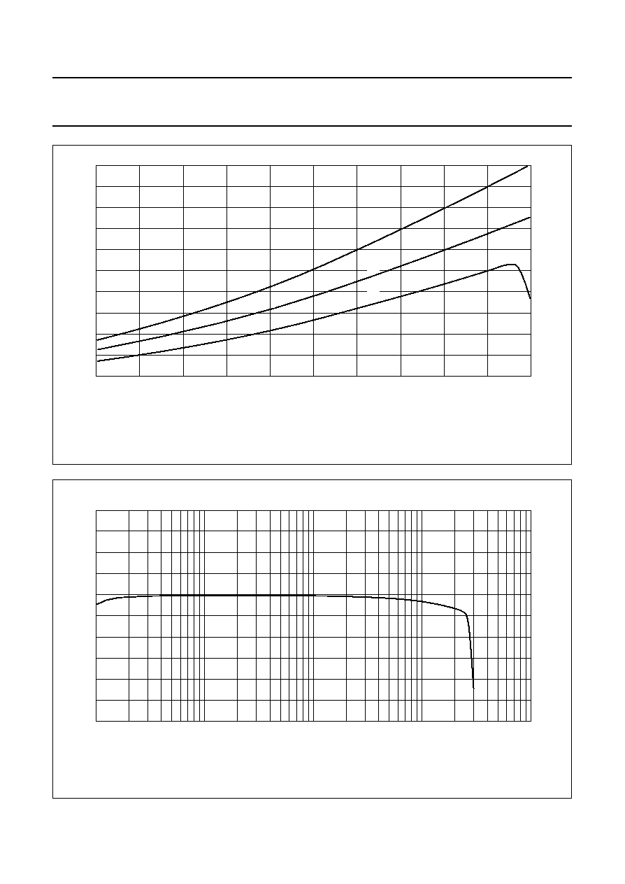
Fig.12 Total harmonic distortion as a function of output power; V
P
= 14.4 V, R
L
= 4
.
(1) f = 10 kHz.
(2) f = 1 kHz.
(3) f = 100 Hz.
10
2
MGA709
10
1
10
1
10
2
10
1
10
P (W)
o
10
2
1
10
2
THD
(%)
(1)
(2)
(3)
July 1994
16
Philips Semiconductors
Preliminary specification
2 x 24 W BTL or 4 x 12 W single-ended car
radio power amplifier
TDA8561Q
handbook, full pagewidth
18
50
0
8
10
12
14
16
MGA710
10
20
30
40
Po
(W)
V (V)
P
(1)
(3)
(2)
Fig.13 Output power as a function of supply voltage.
(1) THD = 30%.
(2) THD = 10%.
(3) THD = 0.5%.
Fig.14 Power bandwidth as a function of frequency; THD = 0.5%, V
P
= 14.4 V, R
L
= 4
.
10
20
10
5
MGA711
10
4
10
3
10
2
10
12
14
16
18
f (Hz)
Po
(W)
July 1994
17
Philips Semiconductors
Preliminary specification
2 x 24 W BTL or 4 x 12 W single-ended car
radio power amplifier
TDA8561Q
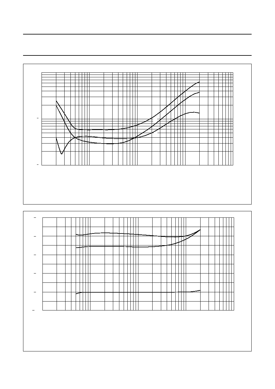
Fig.15 Total harmonic distortion as a function of frequency; V
P
= 14.4 V, R
L
= 4
.
(1) P
O
= 0.1 W.
(2) P
O
= 1 W.
(3) P
O
= 10 W.
10
5
MGA712
10
4
10
3
10
2
10
1
10
2
f (Hz)
10
1
THD
(%)
(1)
(2)
(3)
100
50
10
5
MGA713
10
4
10
3
10
2
10
90
80
70
60
f (Hz)
RR
(dB)
(1)
(2)
(3)
Fig.16 Ripple rejection as a function of frequency.
(1) On condition.
(2) Mute condition.
(3) Stand-by condition.
July 1994
18
Philips Semiconductors
Preliminary specification
2 x 24 W BTL or 4 x 12 W single-ended car
radio power amplifier
TDA8561Q
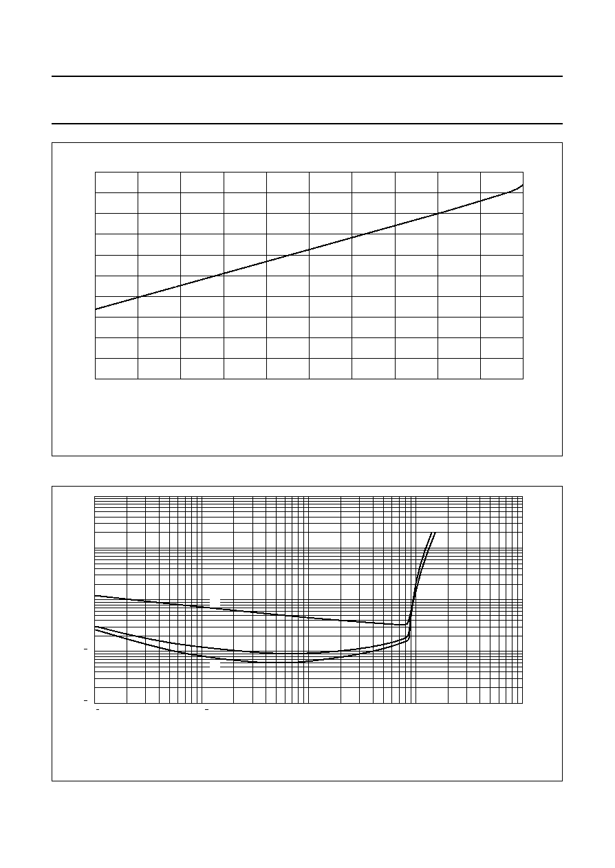
Fig.17 Quiescent current as a function of supply voltage; R
L
=
.
handbook, full pagewidth
18
100
60
8
10
12
14
16
MGA714
68
76
84
92
V (V)
P
Iq
(mA)
SINGLE-ENDED APPLICATION
10
2
MGA715
10
1
10
1
10
2
10
1
10
P (W)
o
10
2
1
10
2
THD
(%)
(2)
(1)
(3)
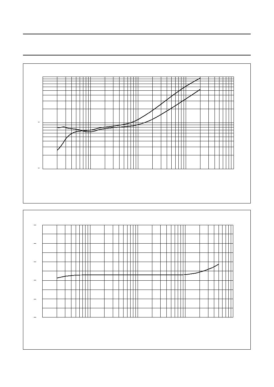
Fig.18 Total harmonic distortion as a function of output power; V
P
= 14.4 V, R
L
= 2
.
(1) f = 10 kHz.
(2) f = 1 kHz.
(3) f = 100 Hz.

July 1994
19
Philips Semiconductors
Preliminary specification
2 x 24 W BTL or 4 x 12 W single-ended car
radio power amplifier
TDA8561Q
Fig.19 Output power as a function of supply voltage.
(1) THD = 30%.
(2) THD = 10%.
(3) THD = 0.5%.
handbook, full pagewidth
18
15
0
8
10
12
14
16
MGA716
3
6
9
12
Po
(W)
V (V)
P
(2)
(3)
(1)
Fig.20 Power bandwidth as a function of frequency; THD = 0.5%, V
P
= 14.4 V, R
L
= 2
.
0
10
10
5
MGA717
10
4
10
3
10
2
10
2
4
6
8
f (Hz)
Po
(W)
July 1994
20
Philips Semiconductors
Preliminary specification
2 x 24 W BTL or 4 x 12 W single-ended car
radio power amplifier
TDA8561Q
Fig.21 Total harmonic distortion as a function of frequency; V
P
= 14.4 V, R
L
= 2
.
(1) P
o
= 0.1 W.
(2) P
o
= 1 W.
10
5
MGA718
10
4
10
3
10
2
10
1
10
2
f (Hz)
10
1
THD
(%)
(1)
(2)
Fig.22 Channel separation as a function of frequency.
handbook, full pagewidth
80
30
10
5
MGA719
10
4
10
3
10
2
10
70
60
50
40
f (Hz)
(dB)
cs

July 1994
21
Philips Semiconductors
Preliminary specification
2 x 24 W BTL or 4 x 12 W single-ended car
radio power amplifier
TDA8561Q
BTL APPLICATION
Fig.23 Total power dissipation as a function of output power; V
P
= 14.4 V, R
L
= 4
(1 channel driven BTL or
4 channels in single-ended mode).
14
2
0
4
MGA720
4
P tot
(W)
P (W)
o
6
8
10
12
8
12
16
20
24
28
July 1994
22
Philips Semiconductors
Preliminary specification
2 x 24 W BTL or 4 x 12 W single-ended car
radio power amplifier
TDA8561Q
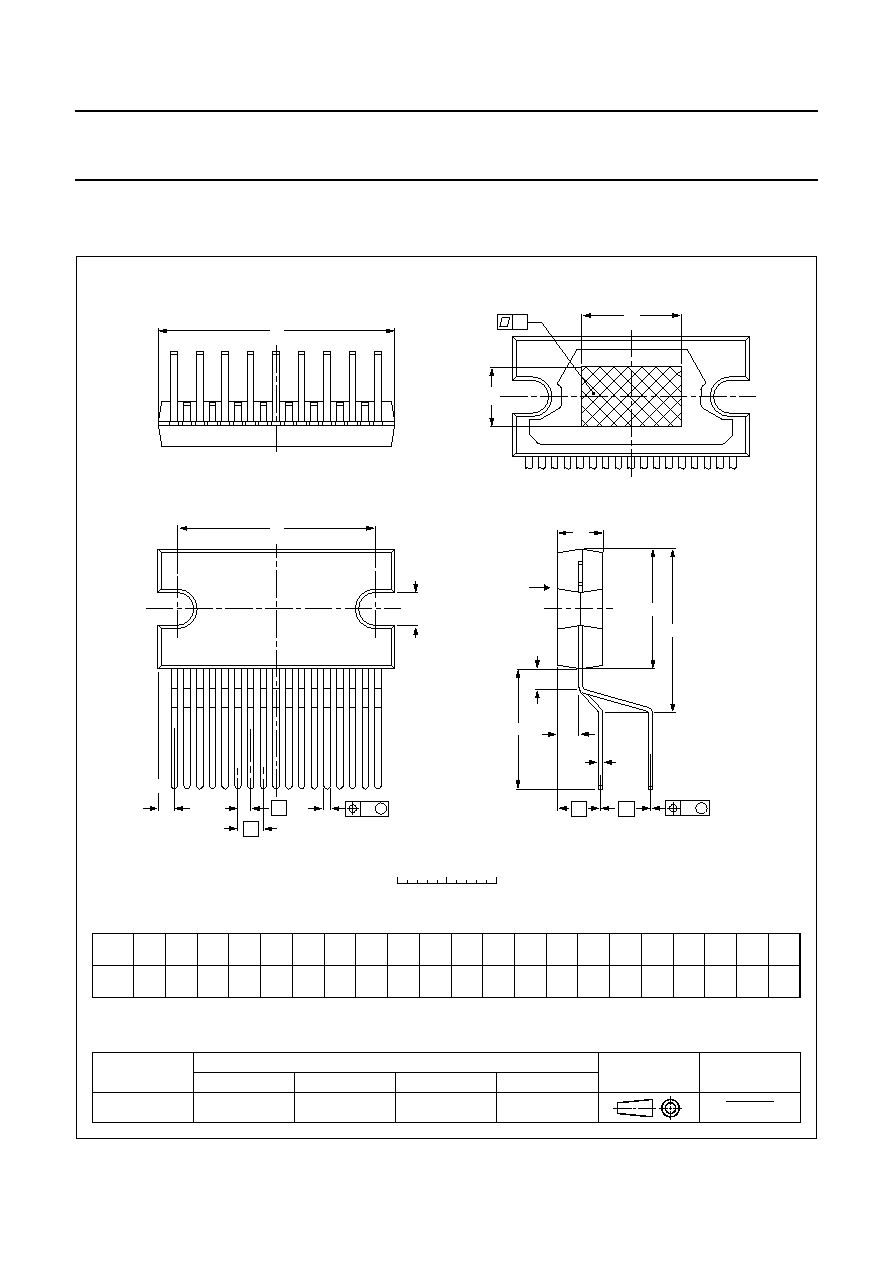
PACKAGE OUTLINE
REFERENCES
OUTLINE
VERSION
EUROPEAN
PROJECTION
ISSUE DATE
IEC
JEDEC
EIAJ
DIMENSIONS (mm are the original dimensions)
Note
1. Plastic or metal protrusions of 0.25 mm maximum per side are not included.
SOT243-1
0
5
10 mm
scale
D
L
E
A
c
A
2
L
3
Q
w
M
b
p
1
d
D
Z
e
e
x
h
1
17
j
Eh
non-concave
92-11-17
95-03-11
DBS17P: plastic DIL-bent-SIL power package; 17 leads (lead length 12 mm)
SOT243-1
view B: mounting base side
m
2
e
v
M
B
UNIT
A
e
1
A
2
b
p
c
D
(1)
E
(1)
Z
(1)
d
e
D
h
L
L
3
m
mm
17.0
15.5
4.6
4.2
0.75
0.60
0.48
0.38
24.0
23.6
20.0
19.6
10
2.54
v
0.8
12.2
11.8
1.27
e
2
5.08
2.4
1.6
E
h
6
2.00
1.45
2.1
1.8
3.4
3.1
4.3
12.4
11.0
Q
j
0.4
w
0.03
x

July 1994
23
Philips Semiconductors
Preliminary specification
2 x 24 W BTL or 4 x 12 W single-ended car
radio power amplifier
TDA8561Q
SOLDERING
Introduction
There is no soldering method that is ideal for all IC
packages. Wave soldering is often preferred when
through-hole and surface mounted components are mixed
on one printed-circuit board. However, wave soldering is
not always suitable for surface mounted ICs, or for
printed-circuits with high population densities. In these
situations reflow soldering is often used.
This text gives a very brief insight to a complex technology.
A more in-depth account of soldering ICs can be found in
our
"IC Package Databook" (order code 9398 652 90011).
Soldering by dipping or by wave
The maximum permissible temperature of the solder is
260
∞
C; solder at this temperature must not be in contact
with the joint for more than 5 seconds. The total contact
time of successive solder waves must not exceed
5 seconds.
The device may be mounted up to the seating plane, but
the temperature of the plastic body must not exceed the
specified maximum storage temperature (T
stg max
). If the
printed-circuit board has been pre-heated, forced cooling
may be necessary immediately after soldering to keep the
temperature within the permissible limit.
Repairing soldered joints
Apply a low voltage soldering iron (less than 24 V) to the
lead(s) of the package, below the seating plane or not
more than 2 mm above it. If the temperature of the
soldering iron bit is less than 300
∞
C it may remain in
contact for up to 10 seconds. If the bit temperature is
between 300 and 400
∞
C, contact may be up to 5 seconds.
DEFINITIONS
LIFE SUPPORT APPLICATIONS
These products are not designed for use in life support appliances, devices, or systems where malfunction of these
products can reasonably be expected to result in personal injury. Philips customers using or selling these products for
use in such applications do so at their own risk and agree to fully indemnify Philips for any damages resulting from such
improper use or sale.
Data sheet status
Objective specification
This data sheet contains target or goal specifications for product development.
Preliminary specification
This data sheet contains preliminary data; supplementary data may be published later.
Product specification
This data sheet contains final product specifications.
Limiting values
Limiting values given are in accordance with the Absolute Maximum Rating System (IEC 134). Stress above one or
more of the limiting values may cause permanent damage to the device. These are stress ratings only and operation
of the device at these or at any other conditions above those given in the Characteristics sections of the specification
is not implied. Exposure to limiting values for extended periods may affect device reliability.
Application information
Where application information is given, it is advisory and does not form part of the specification.