 | –≠–ª–µ–∫—Ç—Ä–æ–Ω–Ω—ã–π –∫–æ–º–ø–æ–Ω–µ–Ω—Ç: TDA8706AM | –°–∫–∞—á–∞—Ç—å:  PDF PDF  ZIP ZIP |

DATA SHEET
Product specification
File under Integrated Circuits, IC02
1996 Jul 30
INTEGRATED CIRCUITS
TDA8706A
6-bit analog-to-digital converter
with multiplexer and clamp
1996 Jul 30
2
Philips Semiconductors
Product specification
6-bit analog-to-digital converter
with multiplexer and clamp
TDA8706A
FEATURES
∑
6-bit resolution
∑
Binary 3-state CMOS outputs
∑
CMOS compatible digital inputs
∑
3 multiplexed video inputs
∑
R, G and B clamps on code 0
∑
Single 6-bit ADC operation allowed up to 40 MSPS
∑
External control of clamping level
∑
Internal reference voltage (external reference allowed)
∑
Power dissipation only 36 mW (typical)
∑
Operating temperature of
-
40 to +85
∞
C
∑
Operating between 2.7 and 5.5 V.
APPLICATIONS
∑
General purpose video applications
∑
R, G and B signals
∑
Automotive (car navigation)
∑
LCD systems
∑
Frame grabber.
GENERAL DESCRIPTION
The TDA8706A is a 6-bit analog-to-digital converter (ADC)
with 3 analog multiplexed inputs. Each input has an analog
clamp on code 0 for RGB video processing. Clamping
level can also be adjusted externally up to code 20. It can
also be used as a single 6-bit ADC.
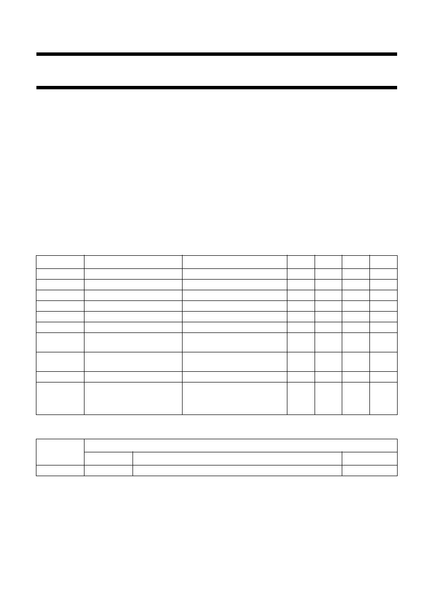
QUICK REFERENCE DATA
ORDERING INFORMATION
SYMBOL
PARAMETER
CONDITIONS
MIN.
TYP.
MAX.
UNIT
V
DDA
analog supply voltage
2.7
3.0
5.5
V
V
DDD
digital supply voltage
2.7
3.0
5.5
V
V
DDO
output stages supply voltage
2.7
3.0
5.5
V
I
DDA
analog supply current
-
7
10
mA
I
DDD
digital supply current
-
4
6
mA
I
DDO
output stages supply current
f
clk
= 40 MHz; ramp input
-
1
1.5
mA
INL
integral non-linearity
f
clk
= 40 MHz; ramp input;
T
amb
= 25
∞
C
-
±
0.25
±
0.6
LSB
DNL
differential non-linearity
f
clk
= 40 MHz; ramp input;
T
amb
= 25
∞
C
-
±
0.20
±
0.5
LSB
f
clk(max)
maximum clock frequency
40
-
-
MHz
P
tot
total power dissipation
f
clk
= 40 MHz; ramp input
3 V supplies
-
36
-
mW
5.5 V supplies
-
-
96
mW
TYPE
NUMBER
PACKAGE
NAME
DESCRIPTION
VERSION
TDA8706AM
SSOP24
plastic shrink small outline package; 24 leads; body width 5.3 mm
SOT340-1

1996 Jul 30
3
Philips Semiconductors
Product specification
6-bit analog-to-digital converter
with multiplexer and clamp
TDA8706A
BLOCK DIAGRAM
Fig.1 Block diagram.
handbook, full pagewidth
MULTIPLEXER
6-BIT
ADC
CMOS
OUTPUTS
REGULATOR
4
8
9
10
22
SR
SG
SB
5
21
23
1
2
3
6
7
14
select
inputs
24
15
13
12
11
D0
16
D1
17
D2
18
D3
19
D4
20
D5
digital
voltage
outputs
MGD133
TDA8706A
CLP
RED
GREEN
BLUE
VSSD
VDDO
VDDA
VDDD
VDDA
VRB
VSSA
VSSO
CLK
VCLPB
VCLPG
VCLPR
CLAMP

1996 Jul 30
4
Philips Semiconductors
Product specification
6-bit analog-to-digital converter
with multiplexer and clamp
TDA8706A
PINNING
SYMBOL
PIN
DESCRIPTION
SR
1
select input RED
SG
2
select input GREEN
SB
3
select input BLUE
CLP
4
clamping pulse input (positive pulse)
V
DDA
5
analog supply voltage
V
RB
6
reference voltage BOTTOM input
V
SSA
7
analog ground
RED
8
RED input
GREEN
9
GREEN input
BLUE
10
BLUE input
V
CLPR
11
RED clamping voltage level input
V
CLPB
12
BLUE clamping voltage level input
V
CLPG
13
GREEN clamping voltage level input
V
SSO
14
digital output ground
D0
15
digital voltage output; bit 0 (LSB)
D1
16
digital voltage output; bit 1
D2
17
digital voltage output; bit 2
D3
18
digital voltage output; bit 3
D4
19
digital voltage output; bit 4
D5
20
digital voltage output; bit 5
V
DDO
21
supply voltage for output stage
V
SSD
22
digital ground
V
DDD
23
digital supply voltage
CLK
24
clock input
Fig.2 Pin configuration.
handbook, halfpage
TDA8706A
MGD132
1
2
3
4
5
6
7
8
9
10
11
12
24 CLK
VDDD
VSSD
VDDO
D5
D4
D3
D2
D1
D0
VSSO
VCLPB
SR
SG
SB
CLP
VDDA
VRB
VSSA
RED
GREEN
BLUE
VCLPR
VCLPG
23
22
21
20
19
18
17
16
15
14
13
1996 Jul 30
5
Philips Semiconductors
Product specification
6-bit analog-to-digital converter
with multiplexer and clamp
TDA8706A
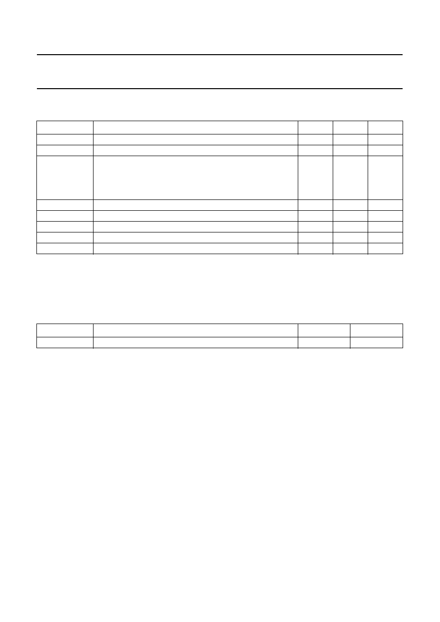
LIMITING VALUES
In accordance with the Absolute Maximum Rating System (IEC 134).
HANDLING
Inputs and outputs are protected against electrostatic discharges in normal handling. However, to be totally safe, it is
desirable to take normal precautions appropriate to handling integrated circuits.
THERMAL CHARACTERISTICS
SYMBOL
PARAMETER
MIN.
MAX.
UNIT
V
DDA
analog supply voltage
-
0.3
+7.0
V
V
DDD
digital supply voltage
-
0.3
+7.0
V
V
DD
supply voltage difference
V
DDA
-
V
DDD
-
1.0
+1.0
V
V
DDA
-
V
DDO
-
1.0
+1.0
V
V
DDD
-
V
DDO
-
1.0
+1.0
V
V
I
input voltage
-
0.3
+7.0
V
I
O
output current
-
10
mA
T
stg
storage temperature
-
55
+150
∞
C
T
amb
operating ambient temperature
-
40
+85
∞
C
T
j
junction temperature
-
+150
∞
C
SYMBOL
PARAMETER
VALUE
UNIT
R
th j-a
thermal resistance from junction to ambient in free air
119
K/W

1996 Jul 30
6
Philips Semiconductors
Product specification
6-bit analog-to-digital converter
with multiplexer and clamp
TDA8706A
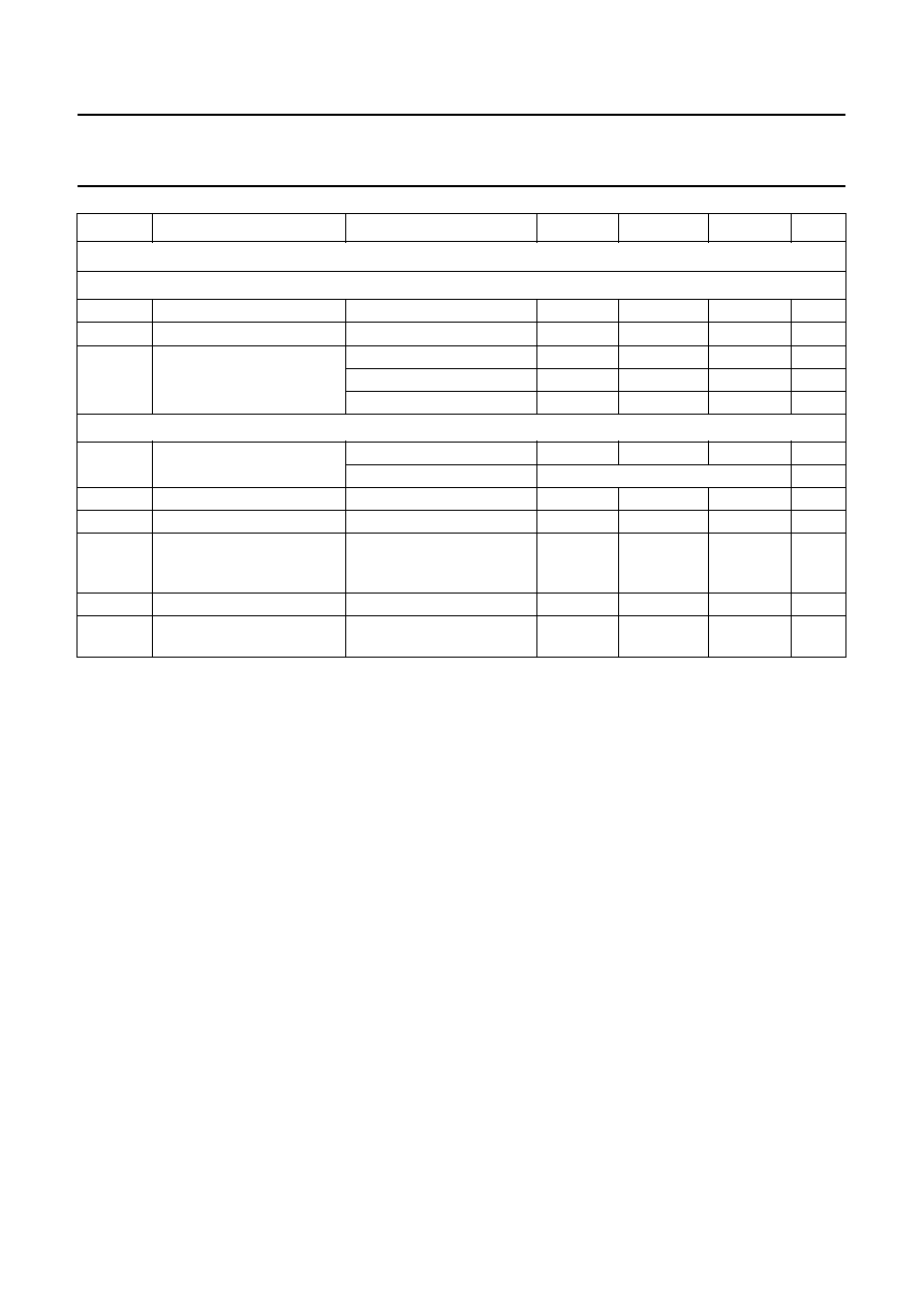
CHARACTERISTICS
V
DDA
= V
5
to V
7
= 2.7 to 5.5 V; V
DDD
= V
23
to V
22
= 2.7 to 5.5 V; V
DDO
= V
21
to V
14
= 2.7 to 5.5 V;
V
SSA
, V
SSD
and V
SSO
shorted together; V
i(p-p)
= 0.7 V; T
amb
=
-
40 to +85
∞
C; typical values measured at
V
DDA
= V
DDD
= V
DDO
= 3 V and T
amb
= 25
∞
C; unless otherwise specified.
SYMBOL
PARAMETER
CONDITIONS
MIN.
TYP.
MAX.
UNIT
Supply
V
DDA
analog supply voltage
2.7
3.0
5.5
V
V
DDD
digital supply voltage
2.7
3.0
5.5
V
V
DDO
output stages supply
voltage
2.7
3.0
5.5
V
V
DD
supply voltage difference
V
DDA
-
V
DDD
-
0.3
-
+0.3
V
V
DDA
-
V
DDO
-
0.3
-
+0.3
V
V
DDD
-
V
DDO
-
0.3
-
+0.3
V
I
DDA
analog supply current
-
7
10
mA
I
DDD
digital supply current
-
4
6
mA
I
DDO
output stages supply current f
clk
= 40 MHz; ramp input
-
1
1.5
mA
Inputs
C
LOCK INPUT
CLK (
REFERENCED TO
V
SSD
); note 1
V
IL
LOW level input voltage
0
-
V
DDD
◊
0.3 V
V
DDD
< 3.3 V
0
-
V
DDD
◊
0.2 V
V
IH
HIGH level input voltage
V
DDD
◊
0.7
-
V
DDD
V
V
DDD
< 3.3 V
V
DDD
◊
0.8
-
V
DDD
V
I
IL
LOW level input current
V
clk
= V
DDD
◊
0.2
-
1
0
+1
µ
A
I
IH
HIGH level input current
V
clk
= V
DDD
◊
0.8
-
2
10
µ
A
Z
i
input impedance
f
clk
= 40 MHz
-
4
-
k
C
I
input capacitance
f
clk
= 40 MHz
-
3
-
pF
I
NPUTS
SR, SG, SB, CLP (
REFERENCED TO
V
SSD
)
V
IL
LOW level input voltage
0
-
V
DDD
◊
0.3 V
V
DDD
< 3.3 V
0
-
V
DDD
◊
0.2 V
V
IH
HIGH level input voltage
V
DDD
◊
0.7
-
V
DDD
V
V
DDD
< 3.3 V
V
DDD
◊
0.8
-
V
DDD
V
I
IL
LOW level input current
V
IL
= V
DDD
◊
0.2
-
1
-
-
µ
A
I
IH
HIGH level input current
V
IH
= V
DDD
◊
0.8
-
-
+1
µ
A
I
NPUTS
V
CLPR
, V
CLPG
AND
V
CLPB
(
REFERENCED TO
V
SSA
); see Tables 1 and 2
V
CLP
input voltage for clamping
V
code
-
9
-
V
code 20
V
I
CLP
input current
-
-
30
µ
A

1996 Jul 30
7
Philips Semiconductors
Product specification
6-bit analog-to-digital converter
with multiplexer and clamp
TDA8706A
A
NALOG INPUTS
RED, GREEN
AND
BLUE; see Table 1
V
i(p-p)
input voltage amplitude
(peak-to-peak value)
V
DDA
= V
DDD
= 3 V;
T
amb
= 25
∞
C
0.665
0.70
0.735
V
V
DDA
= V
DDD
= 5 V;
T
amb
= 25
∞
C
0.625
0.66
0.695
V
I
i
input current
-
-
10
µ
A
C
clamp
clamp coupling capacitance
1
10
100
nF
Reference voltages for the resistor ladder; see Table 1
V
RB
reference voltage BOTTOM
V
DDA
= 3 V
-
V
DDA
-
1.19
-
V
V
DDA
= 5 V
-
V
DDA
-
1.13
-
V
T
VRB
temperature variation on
V
RB
T
amb
= 0 to 50
∞
C
-
0.7
-
mV/
∞
C
Outputs
D
IGITAL OUTPUTS
D5
TO
D0 (
REFERENCED TO
V
SSD
)
V
OL
LOW level output voltage
I
O
= 1 mA
0
-
0.5
V
V
OH
HIGH level output voltage
I
O
=
-
1 mA
V
DDO
-
0.5
-
V
DDO
V
Switching characteristics
C
LOCK INPUT
CLK; see Fig.3; note 1
f
clk(max)
maximum clock frequency
40
-
-
MHz
f
mux(max)
maximum multiplexer
frequency
20
-
-
MHz
t
CPH
clock pulse width HIGH
8
-
-
ns
t
CPL
clock pulse width LOW
8
-
-
ns
t
r
clock rise time
10% to 90%; f
clk
25 MHz;
LOW = V
SSD
, HIGH = V
DDD
-
-
10
ns
t
f
clock fall time
90% to 10%; f
clk
25 MHz;
LOW = V
SSD
, HIGH = V
DDD
-
-
10
ns
Analog signal processing
L
INEARITY
INL
integral non-linearity
f
clk
= 40 MHz; ramp input;
T
amb
= 25
∞
C
-
±
0.25
±
0.6
LSB
DNL
differential non-linearity
f
clk
= 40 MHz; ramp input;
T
amb
= 25
∞
C
-
±
0.20
±
0.5
LSB
E
FFECTIVE BITS
; note 2
EB
effective bits
f
clk
= 40 MHz; f
i
= 4.43 MHz
-
5.8
-
bits
SYMBOL
PARAMETER
CONDITIONS
MIN.
TYP.
MAX.
UNIT
1996 Jul 30
8
Philips Semiconductors
Product specification
6-bit analog-to-digital converter
with multiplexer and clamp
TDA8706A
Notes
1. In addition to a good layout of the digital and analog ground, it is recommended that the rise and fall times of the clock
must not be less than 1 ns.
2. Effective bits are obtained via a Fast Fourier Transform (FFT) treatment taking 8K acquisition points per equivalent
fundamental period. The calculation takes into account all harmonics and noise up to half of the clock frequency
(NYQUIST frequency). Conversion to signal-to-noise ratio: S/N = EB
◊
6.02 + 1.76 dB.
3. Output data acquisition: the output data is available after the maximum delay time of t
d
.
Timing (f
clk
= 40 MHz; C
L
= 20 pF); T
amb
= 25
∞
C; see Fig.3
O
UTPUT DATA
; note 3
t
ds
sampling delay time
-
-
7
ns
t
h
output hold time
5
-
-
ns
t
d
output delay time
V
DDO
= 4.75 V
-
12
15
ns
V
DDO
= 3.15 V
-
17
20
ns
V
DDO
= 2.70 V
-
18
21
ns
S
ELECT INPUT SIGNALS
SR, SG, SB
AND
CLP
t
su
set-up time SR, SG and SB
with no overlap; see Fig.3
10
-
-
ns
with overlap
see Fig.4
ns
t
r
rise time SR, SG and SB
10% to 90%
4
6
-
ns
t
f
fall time SR, SG and SB
90% to 10%
4
6
-
ns
t
over
R, G and B (active) overlap
time with respect to select
signals SR, SG and SB
see Fig.4
0
-
-
ns
t
CLPP
clamp pulse time
C
CLP
= 10 nF
-
3
-
µ
s
t
MH
multiplexer hold time
SR, SG and SB
9
-
-
ns
SYMBOL
PARAMETER
CONDITIONS
MIN.
TYP.
MAX.
UNIT

1996 Jul 30
9
Philips Semiconductors
Product specification
6-bit analog-to-digital converter
with multiplexer and clamp
TDA8706A
Table 1
Output coding and input voltage (typical values)
Table 2
Clamping input level (V
CLPR
, V
CLPG
and V
CLPB
)
Note
1. Use capacitor
10 pF to V
SSA
.
Table 3
Clamp and inputs RED, GREEN and BLUE; V
DDA
= V
DDD
= V
DDO
= 3 V
Note
1. Where X = don't care.
Table 4
Clamping characteristic related to TV signals
STEP
V
i(p-p)
(V)
BINARY OUTPUT BITS
V
DDA
= V
DDD
= 3 V V
DDA
= V
DDD
= 5 V
D5
D4
D3
D2
D1
D0
Underflow
<
V
DDA
-
1.1
<
V
DDA
-
1.06
0
0
0
0
0
0
0
V
DDA
-
1.1
V
DDA
-
1.06
0
0
0
0
0
0
1
.
.
0
0
0
0
0
1
.
.
.
.
.
.
.
.
.
.
.
.
.
.
.
.
.
.
62
.
.
1
1
1
1
1
0
63
V
DDA
-
0.4
V
DDA
-
0.4
1
1
1
1
1
1
Overflow
>
V
DDA
-
0.4
>
V
DDA
-
0.4
1
1
1
1
1
1
V
CLPR
, V
CLPG
AND V
CLPB
CLAMPING LEVEL
Open-circuit
(1)
code 0
V
code
-
9
to V
code 20
code
-
9 to code 20
SR or SG or SB
CLAMP
V
CLPR
, V
CLPG
or V
CLPB
V
i
RED or GREEN or BLUE
DIGITAL OUTPUTS
0
1
open
V
DDA
-
1.1 V
X
(1)
V
CLP
V
CLP
1
open
V
DDA
-
1.1 V
0
V
CLP
V
CLP
code (V
CLP
)
PARAMETER
MIN.
TYP.
MAX.
UNIT
Clamping time per line (signal active)
2.2
3.0
-
µ
s
Input signals clamped to correct level
-
3
10
lines
1996 Jul 30
10
Philips Semiconductors
Product specification
6-bit analog-to-digital converter
with multiplexer and clamp
TDA8706A
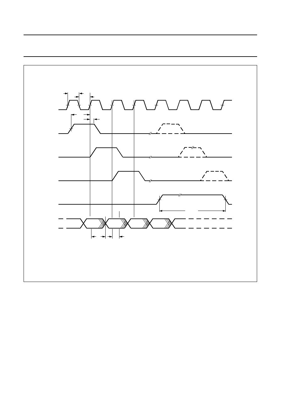
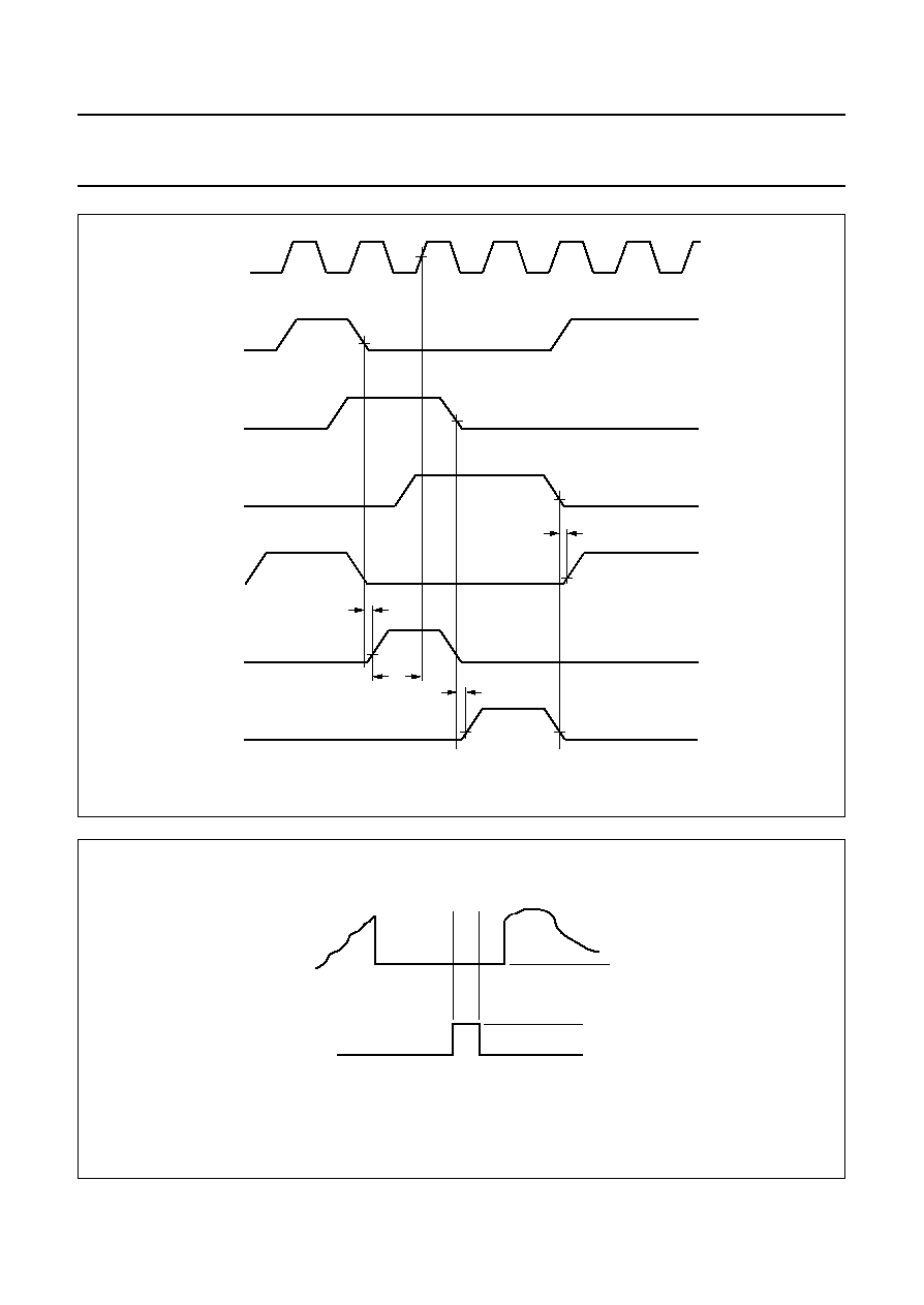
Fig.3 AC characteristics select signals, clamp and output data.
handbook, full pagewidth
MBE859
tCPH
tSU
tMH
td
th
tCLPP
tCPL
CLK
SR
SG
SB
CLAMP
OUTPUT
DATA
GREEN
BLUE
RED
GREEN
1996 Jul 30
11
Philips Semiconductors
Product specification
6-bit analog-to-digital converter
with multiplexer and clamp
TDA8706A
Fig.4 Anti-overlap system for analog multiplexer.
handbook, full pagewidth
MBE860
SR
CLK
SG
SB
RED
ACTIVE
GREEN
ACTIVE
BLUE
ACTIVE
tover
tsu
tover
tover
Fig.5 AC characteristics select signals; clamp and data.
handbook, full pagewidth
1
0
CLAMP
input
RED, GREEN, BLUE
(SR, SG, SB inputs)
digital outputs
= 000000
MBE861

1996 Jul 30
12
Philips Semiconductors
Product specification
6-bit analog-to-digital converter
with multiplexer and clamp
TDA8706A
INTERNAL PIN CONFIGURATIONS
Fig.6 CMOS data outputs.
handbook, halfpage
MGD134
VDDO
VSSO
D5 to D0
Fig.7 V
RB
.
handbook, halfpage
RLAD
MBE967
VRB
VDDA
VSSA
REGULATOR
Fig.8 CLK input.
handbook, halfpage
VDDD
VSSD
CLK
MLC860
1
/
2
VDDD
1996 Jul 30
13
Philips Semiconductors
Product specification
6-bit analog-to-digital converter
with multiplexer and clamp
TDA8706A
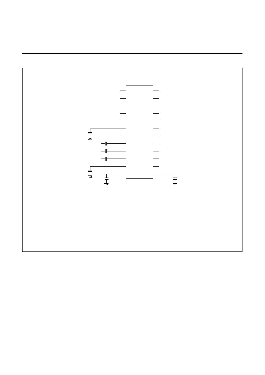
APPLICATION INFORMATION
handbook, full pagewidth
TDA8706A
MBE969
1
2
3
4
5
6
7
8
9
10
11
12
24
CLK
VDDD
VSSD
VDDO
D5
D4
D3
D2
D1
D0
VSSO
VCLPB
(2)
SR
SG
SB
CLP
VDDA
VRB(1)
VSSA
RED
GREEN
BLUE
VCLPR
(2)
VCLPG
(2)
23
22
21
20
19
18
17
16
15
14
13
VSSA
100
nF
VSSA
100
nF
VSSA
100
nF
VSSA
100
nF
The analog and digital supplies should be separated and decoupled.
V
RB
must not be connected to V
CLPR
, V
CLPB
or V
CLPG
pins.
For applications where the black level is clamped to code 0, V
CLPR
, V
CLPB
and V
CLPG
must be left open-circuit with their respective decoupling
capacitors. In that event, they may also be connected together in order to use only one single decoupling capacitor.
(1) V
RB
is decoupled to V
SSA
. Eventually an external regulator can be connected to V
RB
.
(2) V
CLPR
, V
CLPB
and V
CLPG
are decoupled to V
SSA
. Eventually external voltages can be forced on V
CLPR
, V
CLPB
and V
CLPG
.
Fig.9 Application diagram.

1996 Jul 30
14
Philips Semiconductors
Product specification
6-bit analog-to-digital converter
with multiplexer and clamp
TDA8706A
PACKAGE OUTLINE
UNIT
A
1
A
2
A
3
b
p
c
D
(1)
E
(1)
(1)
e
H
E
L
L
p
Q
Z
y
w
v
REFERENCES
OUTLINE
VERSION
EUROPEAN
PROJECTION
ISSUE DATE
IEC
JEDEC
EIAJ
mm
0.21
0.05
1.80
1.65
0.38
0.25
0.20
0.09
8.4
8.0
5.4
5.2
0.65
1.25
7.9
7.6
0.9
0.7
0.8
0.4
8
0
o
o
0.13
0.1
0.2
DIMENSIONS (mm are the original dimensions)
Note
1. Plastic or metal protrusions of 0.20 mm maximum per side are not included.
1.03
0.63
SOT340-1
MO-150AG
93-09-08
95-02-04
X
w
M
A
A
1
A
2
b
p
D
H
E
L
p
Q
detail X
E
Z
e
c
L
v
M
A
(A )
3
A
1
12
24
13
0.25
y
pin 1 index
0
2.5
5 mm
scale
SSOP24: plastic shrink small outline package; 24 leads; body width 5.3 mm
SOT340-1
A
max.
2.0

1996 Jul 30
15
Philips Semiconductors
Product specification
6-bit analog-to-digital converter
with multiplexer and clamp
TDA8706A
SOLDERING
Introduction
There is no soldering method that is ideal for all IC
packages. Wave soldering is often preferred when
through-hole and surface mounted components are mixed
on one printed-circuit board. However, wave soldering is
not always suitable for surface mounted ICs, or for
printed-circuits with high population densities. In these
situations reflow soldering is often used.
This text gives a very brief insight to a complex technology.
A more in-depth account of soldering ICs can be found in
our
"IC Package Databook" (order code 9398 652 90011).
Reflow soldering
Reflow soldering techniques are suitable for all SO and
SSOP packages.
Reflow soldering requires solder paste (a suspension of
fine solder particles, flux and binding agent) to be applied
to the printed-circuit board by screen printing, stencilling or
pressure-syringe dispensing before package placement.
Several techniques exist for reflowing; for example,
thermal conduction by heated belt. Dwell times vary
between 50 and 300 seconds depending on heating
method. Typical reflow temperatures range from
215 to 250
∞
C.
Preheating is necessary to dry the paste and evaporate
the binding agent. Preheating duration: 45 minutes at
45
∞
C.
Wave soldering
SO
Wave soldering techniques can be used for all SO
packages if the following conditions are observed:
∑
A double-wave (a turbulent wave with high upward
pressure followed by a smooth laminar wave) soldering
technique should be used.
∑
The longitudinal axis of the package footprint must be
parallel to the solder flow.
∑
The package footprint must incorporate solder thieves at
the downstream end.
SSOP
Wave soldering is not recommended for SSOP packages.
This is because of the likelihood of solder bridging due to
closely-spaced leads and the possibility of incomplete
solder penetration in multi-lead devices.
If wave soldering cannot be avoided, the following
conditions must be observed:
∑
A double-wave (a turbulent wave with high upward
pressure followed by a smooth laminar wave)
soldering technique should be used.
∑
The longitudinal axis of the package footprint must
be parallel to the solder flow and must incorporate
solder thieves at the downstream end.
Even with these conditions, only consider wave
soldering SSOP packages that have a body width of
4.4 mm, that is SSOP16 (SOT369-1) or
SSOP20 (SOT266-1).
M
ETHOD
(SO
AND
SSOP)
During placement and before soldering, the package must
be fixed with a droplet of adhesive. The adhesive can be
applied by screen printing, pin transfer or syringe
dispensing. The package can be soldered after the
adhesive is cured.
Maximum permissible solder temperature is 260
∞
C, and
maximum duration of package immersion in solder is
10 seconds, if cooled to less than 150
∞
C within
6 seconds. Typical dwell time is 4 seconds at 250
∞
C.
A mildly-activated flux will eliminate the need for removal
of corrosive residues in most applications.
Repairing soldered joints
Fix the component by first soldering two diagonally-
opposite end leads. Use only a low voltage soldering iron
(less than 24 V) applied to the flat part of the lead. Contact
time must be limited to 10 seconds at up to 300
∞
C. When
using a dedicated tool, all other leads can be soldered in
one operation within 2 to 5 seconds between
270 and 320
∞
C.

1996 Jul 30
16
Philips Semiconductors
Product specification
6-bit analog-to-digital converter
with multiplexer and clamp
TDA8706A
DEFINITIONS
LIFE SUPPORT APPLICATIONS
These products are not designed for use in life support appliances, devices, or systems where malfunction of these
products can reasonably be expected to result in personal injury. Philips customers using or selling these products for
use in such applications do so at their own risk and agree to fully indemnify Philips for any damages resulting from such
improper use or sale.
Data sheet status
Objective specification
This data sheet contains target or goal specifications for product development.
Preliminary specification
This data sheet contains preliminary data; supplementary data may be published later.
Product specification
This data sheet contains final product specifications.
Limiting values
Limiting values given are in accordance with the Absolute Maximum Rating System (IEC 134). Stress above one or
more of the limiting values may cause permanent damage to the device. These are stress ratings only and operation
of the device at these or at any other conditions above those given in the Characteristics sections of the specification
is not implied. Exposure to limiting values for extended periods may affect device reliability.
Application information
Where application information is given, it is advisory and does not form part of the specification.

1996 Jul 30
17
Philips Semiconductors
Product specification
6-bit analog-to-digital converter
with multiplexer and clamp
TDA8706A
NOTES

1996 Jul 30
18
Philips Semiconductors
Product specification
6-bit analog-to-digital converter
with multiplexer and clamp
TDA8706A
NOTES

1996 Jul 30
19
Philips Semiconductors
Product specification
6-bit analog-to-digital converter
with multiplexer and clamp
TDA8706A
NOTES

Internet: http://www.semiconductors.philips.com
(1)
TDA8706A_1 July 18, 1996 12:44 pm
Philips Semiconductors ≠ a worldwide company
© Philips Electronics N.V. 1996
SCA51
All rights are reserved. Reproduction in whole or in part is prohibited without the prior written consent of the copyright owner.
The information presented in this document does not form part of any quotation or contract, is believed to be accurate and reliable and may be changed
without notice. No liability will be accepted by the publisher for any consequence of its use. Publication thereof does not convey nor imply any license
under patent- or other industrial or intellectual property rights.
Netherlands: Postbus 90050, 5600 PB EINDHOVEN, Bldg. VB,
Tel. +31 40 27 82785, Fax. +31 40 27 88399
New Zealand: 2 Wagener Place, C.P.O. Box 1041, AUCKLAND,
Tel. +64 9 849 4160, Fax. +64 9 849 7811
Norway: Box 1, Manglerud 0612, OSLO,
Tel. +47 22 74 8000, Fax. +47 22 74 8341
Philippines: Philips Semiconductors Philippines Inc.,
106 Valero St. Salcedo Village, P.O. Box 2108 MCC, MAKATI,
Metro MANILA, Tel. +63 2 816 6380, Fax. +63 2 817 3474
Poland: Ul. Lukiska 10, PL 04-123 WARSZAWA,
Tel. +48 22 612 2831, Fax. +48 22 612 2327
Portugal: see Spain
Romania: see Italy
Russia: Philips Russia, Ul. Usatcheva 35A, 119048 MOSCOW,
Tel. +7 095 926 5361, Fax. +7 095 564 8323
Singapore: Lorong 1, Toa Payoh, SINGAPORE 1231,
Tel. +65 350 2538, Fax. +65 251 6500
Slovakia: see Austria
Slovenia: see Italy
South Africa: S.A. PHILIPS Pty Ltd., 195-215 Main Road Martindale,
2092 JOHANNESBURG, P.O. Box 7430 Johannesburg 2000,
Tel. +27 11 470 5911, Fax. +27 11 470 5494
South America: Rua do Rocio 220, 5th floor, Suite 51,
04552-903 S„o Paulo, S√O PAULO - SP, Brazil,
Tel. +55 11 821 2333, Fax. +55 11 829 1849
Spain: Balmes 22, 08007 BARCELONA,
Tel. +34 3 301 6312, Fax. +34 3 301 4107
Sweden: Kottbygatan 7, Akalla, S-16485 STOCKHOLM,
Tel. +46 8 632 2000, Fax. +46 8 632 2745
Switzerland: Allmendstrasse 140, CH-8027 ZÐRICH,
Tel. +41 1 488 2686, Fax. +41 1 481 7730
Taiwan: PHILIPS TAIWAN Ltd., 23-30F, 66,
Chung Hsiao West Road, Sec. 1, P.O. Box 22978,
TAIPEI 100, Tel. +886 2 382 4443, Fax. +886 2 382 4444
Thailand: PHILIPS ELECTRONICS (THAILAND) Ltd.,
209/2 Sanpavuth-Bangna Road Prakanong, BANGKOK 10260,
Tel. +66 2 745 4090, Fax. +66 2 398 0793
Turkey: Talatpasa Cad. No. 5, 80640 GÐLTEPE/ISTANBUL,
Tel. +90 212 279 2770, Fax. +90 212 282 6707
Ukraine: PHILIPS UKRAINE, 4 Patrice Lumumba str., Building B, Floor 7,
252042 KIEV, Tel. +380 44 264 2776, Fax. +380 44 268 0461
United Kingdom: Philips Semiconductors Ltd., 276 Bath Road, Hayes,
MIDDLESEX UB3 5BX, Tel. +44 181 730 5000, Fax. +44 181 754 8421
United States: 811 East Arques Avenue, SUNNYVALE, CA 94088-3409,
Tel. +1 800 234 7381
Uruguay: see South America
Vietnam: see Singapore
Yugoslavia: PHILIPS, Trg N. Pasica 5/v, 11000 BEOGRAD,
Tel. +381 11 825 344, Fax.+381 11 635 777
For all other countries apply to: Philips Semiconductors, Marketing & Sales Communications,
Building BE-p, P.O. Box 218, 5600 MD EINDHOVEN, The Netherlands, Fax. +31 40 27 24825
Argentina: see South America
Australia: 34 Waterloo Road, NORTH RYDE, NSW 2113,
Tel. +61 2 9805 4455, Fax. +61 2 9805 4466
Austria: Computerstr. 6, A-1101 WIEN, P.O. Box 213,
Tel. +43 1 60 101, Fax. +43 1 60 101 1210
Belarus: Hotel Minsk Business Center, Bld. 3, r. 1211, Volodarski Str. 6,
220050 MINSK, Tel. +375 172 200 733, Fax. +375 172 200 773
Belgium: see The Netherlands
Brazil: see South America
Bulgaria: Philips Bulgaria Ltd., Energoproject, 15th floor,
51 James Bourchier Blvd., 1407 SOFIA,
Tel. +359 2 689 211, Fax. +359 2 689 102
Canada: PHILIPS SEMICONDUCTORS/COMPONENTS,
Tel. +1 800 234 7381
China/Hong Kong: 501 Hong Kong Industrial Technology Centre,
72 Tat Chee Avenue, Kowloon Tong, HONG KONG,
Tel. +852 2319 7888, Fax. +852 2319 7700
Colombia: see South America
Czech Republic: see Austria
Denmark: Prags Boulevard 80, PB 1919, DK-2300 COPENHAGEN S,
Tel. +45 32 88 2636, Fax. +45 31 57 1949
Finland: Sinikalliontie 3, FIN-02630 ESPOO,
Tel. +358 615 800, Fax. +358 615 80920
France: 4 Rue du Port-aux-Vins, BP317, 92156 SURESNES Cedex,
Tel. +33 1 40 99 6161, Fax. +33 1 40 99 6427
Germany: Hammerbrookstraþe 69, D-20097 HAMBURG,
Tel. +49 40 23 53 60, Fax. +49 40 23 536 300
Greece: No. 15, 25th March Street, GR 17778 TAVROS,
Tel. +30 1 4894 339/911, Fax. +30 1 4814 240
Hungary: see Austria
India: Philips INDIA Ltd, Shivsagar Estate, A Block, Dr. Annie Besant Rd.
Worli, MUMBAI 400 018, Tel. +91 22 4938 541, Fax. +91 22 4938 722
Indonesia: see Singapore
Ireland: Newstead, Clonskeagh, DUBLIN 14,
Tel. +353 1 7640 000, Fax. +353 1 7640 200
Israel: RAPAC Electronics, 7 Kehilat Saloniki St, TEL AVIV 61180,
Tel. +972 3 645 0444, Fax. +972 3 649 1007
Italy: PHILIPS SEMICONDUCTORS, Piazza IV Novembre 3,
20124 MILANO, Tel. +39 2 6752 2531, Fax. +39 2 6752 2557
Japan: Philips Bldg 13-37, Kohnan 2-chome, Minato-ku, TOKYO 108,
Tel. +81 3 3740 5130, Fax. +81 3 3740 5077
Korea: Philips House, 260-199 Itaewon-dong, Yongsan-ku, SEOUL,
Tel. +82 2 709 1412, Fax. +82 2 709 1415
Malaysia: No. 76 Jalan Universiti, 46200 PETALING JAYA, SELANGOR,
Tel. +60 3 750 5214, Fax. +60 3 757 4880
Mexico: 5900 Gateway East, Suite 200, EL PASO, TEXAS 79905,
Tel. +9-5 800 234 7381
Middle East: see Italy
Printed in The Netherlands
537021/30/01/pp20
Date of release: 1996 Jul 30
Document order number:
9397 750 00991