Document Outline
- FEATURES
- APPLICATIONS
- GENERAL DESCRIPTION
- QUICK REFERENCE DATA
- ORDERING INFORMATION
- BLOCK DIAGRAM
- PINNING
- LIMITING VALUES
- HANDLING
- THERMAL CHARACTERISTICS
- CHARACTERISTICS
- INTERNAL PIN CONFIGURATIONS
- APPLICATION INFORMATION
- PACKAGE OUTLINE
- SOLDERING
- Introduction to soldering surface mount packages
- Reflow soldering
- Wave soldering
- Manual soldering
- Suitability of surface mount IC packages for wave and reflow soldering methods
- DATA SHEET STATUS
- DEFINITIONS
- DISCLAIMERS

DATA SHEET
Product specification
Supersedes data of 1996 Jul 30
2003 Jul 21
INTEGRATED CIRCUITS
TDA8706A
6-bit analog-to-digital converter
with multiplexer and clamp
2003 Jul 21
2
Philips Semiconductors
Product specification
6-bit analog-to-digital converter
with multiplexer and clamp
TDA8706A
FEATURES
∑
6-bit resolution
∑
Binary CMOS compatible outputs
∑
CMOS compatible digital inputs
∑
TLL clock input
∑
Three multiplexed video inputs
∑
R, G and B clamps on code 0
∑
Single 6-bit Analog-to-Digital Converter (ADC) operation
allowed up to 40 MSPS
∑
External control of clamping level
∑
Internal reference voltage (external reference allowed)
∑
Power dissipation only 36 mW (typical)
∑
Operating temperature of
-
40 to +85
∞
C
∑
Operating between 2.7 and 3.6 V
∑
Sine wave clock allowed.
APPLICATIONS
∑
General purpose video applications
∑
R, G and B signals
∑
Automotive (car navigation)
∑
LCD systems
∑
Frame grabber.
GENERAL DESCRIPTION
The TDA8706A is a 6-bit ADC with three analog
multiplexed inputs. Each input has an analog clamp on
code 0 for RGB video processing. Clamping level can also
be adjusted externally up to code 20. It can also be used
as a single 6-bit ADC.
QUICK REFERENCE DATA
ORDERING INFORMATION
SYMBOL
PARAMETER
CONDITIONS
MIN.
TYP.
MAX.
UNIT
V
DDA
analog supply voltage
2.7
3.3
3.6
V
V
DDD
digital supply voltage
2.7
3.3
3.6
V
V
DDO
output stage supply voltage
2.7
3.3
3.6
V
I
DDA
analog supply current
-
6.4
10
mA
I
DDD
digital supply current
-
4.4
8.5
mA
I
DDO
output stage supply current
f
clk
= 40 MHz; ramp input
-
-
1.8
mA
INL
integral non-linearity
f
clk
= 40 MHz; ramp input
-
±
0.20
±
0.5
LSB
DNL
differential non-linearity
f
clk
= 40 MHz; ramp input
-
±
0.10
±
0.35
LSB
f
clk(max)
maximum clock frequency
40
-
-
MHz
P
tot
total power dissipation
f
clk
= 40 MHz; ramp input
-
36
73
mW
TYPE
NUMBER
PACKAGE
NAME
DESCRIPTION
VERSION
TDA8706AM
SSOP24
plastic shrink small outline package; 24 leads; body width 5.3 mm
SOT340-1

2003 Jul 21
3
Philips Semiconductors
Product specification
6-bit analog-to-digital converter
with multiplexer and clamp
TDA8706A
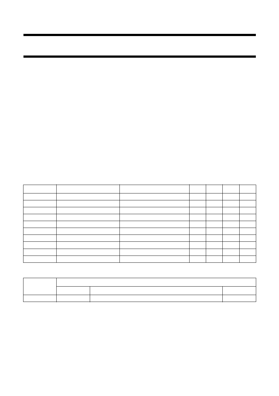
BLOCK DIAGRAM
handbook, full pagewidth
MULTIPLEXER
6-BIT
ADC
CMOS
OUTPUTS
REGULATOR
4
8
9
10
22
SR
SG
SB
5
21
23
1
2
3
6
7
14
select
inputs
24
15
13
12
11
D0
16 D1
17 D2
18 D3
19 D4
20 D5
digital
voltage
outputs
MGD133
TDA8706A
CLP
RED
GREEN
BLUE
VSSD
VDDO
VDDA
VDDD
VDDA
VRB
VSSA
VSSO
CLK
VCLPB
VCLPG
VCLPR
CLAMP
Fig.1 Block diagram.

2003 Jul 21
4
Philips Semiconductors
Product specification
6-bit analog-to-digital converter
with multiplexer and clamp
TDA8706A
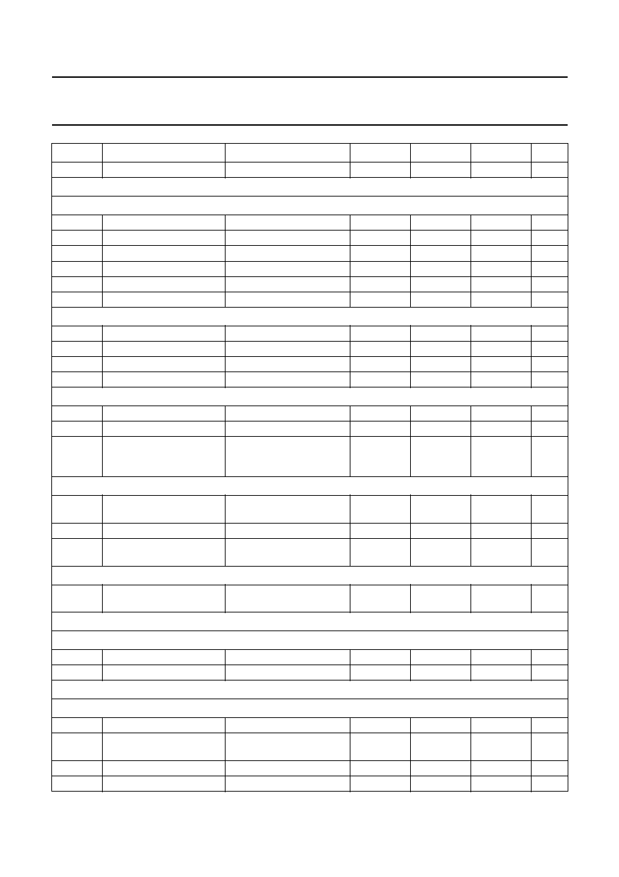
PINNING
SYMBOL
PIN
DESCRIPTION
SR
1
select input RED
SG
2
select input GREEN
SB
3
select input BLUE
CLP
4
clamping pulse input (positive pulse)
V
DDA
5
analog supply voltage
V
RB
6
reference voltage BOTTOM output
V
SSA
7
analog ground
RED
8
RED input
GREEN
9
GREEN input
BLUE
10
BLUE input
V
CLPR
11
RED clamping voltage level input
V
CLPB
12
BLUE clamping voltage level input
V
CLPG
13
GREEN clamping voltage level input
V
SSO
14
output stage ground
D0
15
digital voltage output; bit 0 (LSB)
D1
16
digital voltage output; bit 1
D2
17
digital voltage output; bit 2
D3
18
digital voltage output; bit 3
D4
19
digital voltage output; bit 4
D5
20
digital voltage output; bit 5
V
DDO
21
output stage supply voltage
V
SSD
22
digital ground
V
DDD
23
digital supply voltage
CLK
24
clock input
handbook, halfpage
TDA8706AM
MGD132
1
2
3
4
5
6
7
8
9
10
11
12
24 CLK
VDDD
VSSD
VDDO
D5
D4
D3
D2
D1
D0
VSSO
VCLPB
SR
SG
SB
CLP
VDDA
VRB
VSSA
RED
GREEN
BLUE
VCLPR
VCLPG
23
22
21
20
19
18
17
16
15
14
13
Fig.2 Pin configuration.

2003 Jul 21
5
Philips Semiconductors
Product specification
6-bit analog-to-digital converter
with multiplexer and clamp
TDA8706A
LIMITING VALUES
In accordance with the Absolute Maximum Rating System (IEC 60134).
HANDLING
Inputs and outputs are protected against electrostatic discharge in normal handling. However, to be totally safe, it is
desirable to take normal precautions appropriate to handling integrated circuits.
THERMAL CHARACTERISTICS
CHARACTERISTICS
V
DDA
= 2.7 to 3.6 V; V
DDD
= 2.7 to 3.6 V; V
DDO
= 2.7 to 3.6 V; V
SSA
, V
SSD
and V
SSO
shorted together; V
i(p-p)
= 0.7 V;
T
amb
=
-
40 to +85
∞
C; typical values measured at V
DDA
= V
DDD
= V
DDO
= 3.3 V and T
amb
= 25
∞
C; unless otherwise
specified.
SYMBOL
PARAMETER
MIN.
MAX.
UNIT
V
DDA
analog supply voltage
-
0.3
+7.0
V
V
DDD
digital supply voltage
-
0.3
+7.0
V
V
DD
supply voltage difference
V
DDA
-
V
DDD
-
1.0
+1.0
V
V
DDA
-
V
DDO
-
1.0
+1.0
V
V
DDD
-
V
DDO
-
1.0
+1.0
V
V
I
input voltage
-
0.3
+7.0
V
I
O
output current
-
10
mA
T
stg
storage temperature
-
55
+150
∞
C
T
amb
operating ambient temperature
-
40
+85
∞
C
T
j
junction temperature
-
150
∞
C
SYMBOL
PARAMETER
CONDITIONS
VALUE
UNIT
R
th(j-a)
thermal resistance from junction to
ambient
in free air
119
K/W
SYMBOL
PARAMETER
CONDITIONS
MIN.
TYP.
MAX.
UNIT
Supply
V
DDA
analog supply voltage
2.7
3.3
3.6
V
V
DDD
digital supply voltage
2.7
3.3
3.6
V
V
DDO
output stage supply
voltage
2.7
3.3
3.6
V
V
DD
supply voltage difference
V
DDA
-
V
DDD
-
0.3
-
+0.3
V
V
DDA
-
V
DDO
-
0.3
-
+0.3
V
V
DDD
-
V
DDO
-
0.3
-
+0.3
V
I
DDA
analog supply current
-
6.4
10
mA
I
DDD
digital supply current
-
4.4
8.5
mA
I
DDO
output stage supply
current
f
clk
= 40 MHz; ramp input
-
-
1.8
mA
2003 Jul 21
6
Philips Semiconductors
Product specification
6-bit analog-to-digital converter
with multiplexer and clamp
TDA8706A
P
tot
total power dissipation
-
36
73
mW
Inputs
C
LOCK INPUT
CLK (
REFERENCED TO
V
SSD
); note 1
V
IL
LOW-level input voltage
0
-
0.8
V
V
IH
HIGH-level input voltage
2.0
-
V
DDD
V
I
IL
LOW-level input current
V
clk
= 0.8 V
-
1
0
+1
µ
A
I
IH
HIGH-level input current
V
clk
= 2.0 V
-
2
10
µ
A
Z
i
input impedance
f
clk
= 40 MHz
-
4
-
k
C
i
input capacitance
f
clk
= 40 MHz
-
3
-
pF
I
NPUTS
SR, SG, SB
AND
CLP (
REFERENCED TO
V
SSD
)
V
IL
LOW-level input voltage
0
-
V
DDD
◊
0.3
V
V
IH
HIGH-level input voltage
V
DDD
◊
0.7
-
V
DDD
V
I
IL
LOW-level input current
V
IL
= V
DDD
◊
0.2
-
1
-
-
µ
A
I
IH
HIGH-level input current
V
IH
= V
DDD
◊
0.8
-
-
+1
µ
A
I
NPUTS
V
CLPR
, V
CLPG
AND
V
CLPB
(
REFERENCED TO
V
SSA
); see Tables 1 and 2
V
CLP
input voltage for clamping
V
code
(-
9)
-
V
code(20)
V
I
CLP
input current
-
-
30
µ
A
A
CLP
clamp accuracy
between inputs RED,
GREEN and BLUE of each
device; T
amb
= 25
∞
C
-
1
-
+1
LSB
A
NALOG INPUTS
RED, GREEN
AND
BLUE; see Table 1
V
i(p-p)
input voltage amplitude
(peak-to-peak value)
0.63
0.70
0.77
V
I
i
input current
-
-
10
µ
A
C
clamp
clamp coupling
capacitance
1
10
100
nF
Reference voltages for the resistor ladder; see Table 1
V
RB
BOTTOM reference
voltage
V
DDA
-
1.29 V
DDA
-
1.21 V
DDA
-
1.13 V
Outputs
D
IGITAL OUTPUTS
D5
TO
D0 (
REFERENCED TO
V
SSD
)
V
OL
LOW-level output voltage
I
O
= 1 mA
0
-
0.5
V
V
OH
HIGH-level output voltage
I
O
=
-
1 mA
V
DDO
-
0.5
-
V
DDO
V
Switching characteristics
C
LOCK INPUT
CLK; see Fig.3; note 1
f
clk(max)
maximum clock frequency
40
-
-
MHz
f
mux(max)
maximum multiplexer
frequency
20
-
-
MHz
t
CPH
clock pulse width HIGH
9
-
-
ns
t
CPL
clock pulse width LOW
9
-
-
ns
SYMBOL
PARAMETER
CONDITIONS
MIN.
TYP.
MAX.
UNIT

2003 Jul 21
7
Philips Semiconductors
Product specification
6-bit analog-to-digital converter
with multiplexer and clamp
TDA8706A
Notes
1. In addition to a good layout of the digital and analog ground, it is recommended that the rise and fall times of the clock
must not be less than 1 ns. A sine wave with specified amplitude is also allowed.
2. Effective bits are derived from a Fast Fourier Transform (FFT) processing taking 2K acquisition points per equivalent
fundamental period. The calculation takes into account all harmonics and noise up to half of the clock frequency
(NYQUIST frequency). Conversion to signal-to-noise ratio: S/N = EB
◊
6.02 + 1.76 dB.
3. Output data acquisition: the output data is available after the maximum delay time t
d
.
t
r
clock rise time
10% to 90%; f
clk
40 MHz;
LOW = 0.8 V,
HIGH = 2.0 V
-
-
7
ns
t
f
clock fall time
90% to 10%; f
clk
40 MHz;
LOW = 0.8 V,
HIGH = 2.0 V
-
-
7
ns
Analog signal processing
L
INEARITY
INL
integral non-linearity
f
clk
= 40 MHz; ramp input
-
±
0.20
±
0.5
LSB
DNL
differential non-linearity
f
clk
= 40 MHz; ramp input
-
±
0.10
±
0.35
LSB
E
FFECTIVE BITS
; note 2
EB
effective bits
f
clk
= 40 MHz;
f
i
= 4.43 MHz
5.5
5.8
-
bits
Timing (f
clk
= 40 MHz; C
L
= 10 pF); see Fig.3
O
UTPUT DATA
; note 3
t
ds
sampling delay time
-
-
7
ns
t
h
output hold time
6.5
9.0
-
ns
t
d
output delay time
-
12
19
ns
S
ELECT INPUT SIGNALS
SR, SG, SB
AND
CLP
t
su
set-up time SR, SG and
SB
with no overlap; see Fig.3
10
-
-
ns
with overlap; see Fig.4
-
-
-
ns
t
r
rise time SR, SG and SB
10% to 90%
4
6
-
ns
t
f
fall time SR, SG and SB
90% to 10%
4
6
-
ns
t
over
RED, GREEN and BLUE
(active) overlap time with
respect to select signals
SR, SG and SB
see Fig.4
0
-
-
ns
t
CLPP
clamp pulse time
C
CLP
= 10 nF
-
3
-
µ
s
t
MH
multiplexer hold time SR,
SG and SB
9
-
-
ns
SYMBOL
PARAMETER
CONDITIONS
MIN.
TYP.
MAX.
UNIT
2003 Jul 21
8
Philips Semiconductors
Product specification
6-bit analog-to-digital converter
with multiplexer and clamp
TDA8706A
Table 1
Output coding and input voltage (typical values); V
DDA
= V
DDD
= 3.3 V
Table 2
Clamping input level (V
CLPR
, V
CLPG
and V
CLPB
)
Note
1. Use capacitor
10 pF to V
SSA
.
Table 3
Clamp and inputs RED, GREEN and BLUE; V
DDA
= V
DDD
= V
DDO
= 3.3 V
STEP
V
i
(V)
BINARY OUTPUT BITS
D5
D4
D3
D2
D1
D0
Underflow
<
V
DDA
-
1.12
0
0
0
0
0
0
0
V
DDA
-
1.12
0
0
0
0
0
0
1
.
0
0
0
0
0
1
.
.
.
.
.
.
.
.
.
.
.
.
.
.
.
.
62
.
1
1
1
1
1
0
63
V
DDA
-
0.42
1
1
1
1
1
1
Overflow
>
V
DDA
-
0.42
1
1
1
1
1
1
V
CLPR
, V
CLPG
, V
CLPB
CLAMPING LEVEL
Open-circuit
(1)
code 0
V
code(
-
9)
to V
code(20)
code
-
9 to code 20
SR or SG or SB
CLAMP
V
CLPR
, V
CLPG
or V
CLPB
V
i
RED or GREEN or BLUE
DIGITAL OUTPUTS
0
1
open
V
DDA
-
1.12 V
don't care
V
CLP
V
CLP
1
open
V
DDA
-
1.12 V
0
V
CLP
V
CLP
code (V
CLP
)

2003 Jul 21
9
Philips Semiconductors
Product specification
6-bit analog-to-digital converter
with multiplexer and clamp
TDA8706A
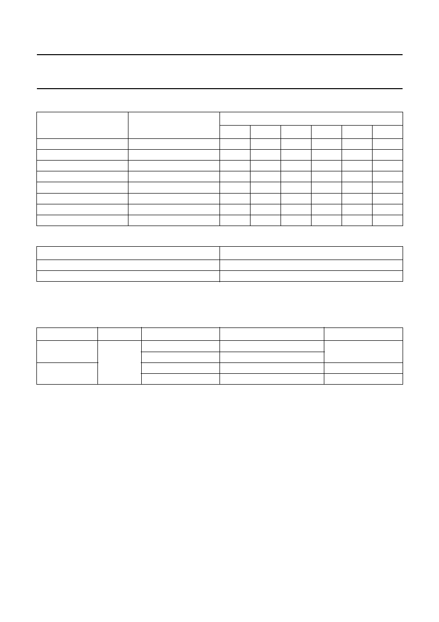
Fig.3 AC characteristics select signals, clamp and output data.
handbook, full pagewidth
MBE859
tCPH
tSU
tMH
1.4 V
td
th
tCLPP
tCPL
CLK
SR
SG
SB
CLAMP
OUTPUT
DATA
GREEN
BLUE
RED
GREEN

2003 Jul 21
10
Philips Semiconductors
Product specification
6-bit analog-to-digital converter
with multiplexer and clamp
TDA8706A
Fig.4 Anti-overlap system for analog multiplexer.
handbook, full pagewidth
MBE860
SR
CLK
SG
SB
RED
ACTIVE
GREEN
ACTIVE
BLUE
ACTIVE
tover
tsu
tover
tover
Fig.5 AC characteristics select signals; clamp and data.
handbook, full pagewidth
1
0
CLAMP
input
RED, GREEN, BLUE
(SR, SG, SB inputs)
digital outputs
= 000000
MBE861

2003 Jul 21
11
Philips Semiconductors
Product specification
6-bit analog-to-digital converter
with multiplexer and clamp
TDA8706A
INTERNAL PIN CONFIGURATIONS
Fig.6 CMOS data outputs pins D0 to D5.
handbook, halfpage
MGD134
VDDO
VSSO
D5 to D0
Fig.7 Output pin V
RB
.
handbook, halfpage
RLAD
MBE967
VRB
VDDA
VSSA
REGULATOR
Fig.8 Input pin CLK.
handbook, halfpage
VDDD
VSSD
CLK
MGX350
1.4 V

2003 Jul 21
12
Philips Semiconductors
Product specification
6-bit analog-to-digital converter
with multiplexer and clamp
TDA8706A
APPLICATION INFORMATION
handbook, full pagewidth
TDA8706A
MBE969
1
2
3
4
5
6
7
8
9
10
11
12
24
CLK
VDDD
(3)
VSSD
VDDO
(3)
D5
D4
D3
D2
D1
D0
VSSO
VCLPB
(2)
SR
SG
SB
CLP
VDDA
VRB
(1)
VSSA
RED
GREEN
BLUE
VCLPR
(2)
VCLPG
(2)
23
22
21
20
19
18
17
16
15
14
13
VSSA
100 nF
VSSA
100 nF
VSSA
VSSA
100 nF
100
nF
100 nF
100 nF
100 nF
The analog and digital supplies should be separated and decoupled.
V
DDO
should be well decoupled with its capacitor in order to be as close as possible to its pin.
V
RB
must not be connected to V
CLPR
, V
CLPB
or V
CLPG
pins.
For applications where the black level is clamped to code 0, V
CLPR
, V
CLPB
and V
CLPG
must be left open-circuit with their respective decoupling
capacitors. In that event, they may also be connected together in order to use only one single decoupling capacitor.
(1) V
RB
is decoupled to V
SSA
. An external regulator can also be connected to V
RB
.
(2) V
CLPR
, V
CLPB
and V
CLPG
are decoupled to V
SSA
. External voltages can also be forced on V
CLPR
, V
CLPB
and V
CLPG
.
(3) V
DDO
and V
DDO
can be shorted together but the decoupling capacitors should remain as close as possible to its pin.
Fig.9 Application diagram.

2003 Jul 21
13
Philips Semiconductors
Product specification
6-bit analog-to-digital converter
with multiplexer and clamp
TDA8706A
PACKAGE OUTLINE
UNIT
A
1
A
2
A
3
b
p
c
D
(1)
E
(1)
(1)
e
H
E
L
L
p
Q
Z
y
w
v
REFERENCES
OUTLINE
VERSION
EUROPEAN
PROJECTION
ISSUE DATE
IEC
JEDEC
JEITA
mm
0.21
0.05
1.80
1.65
0.38
0.25
0.20
0.09
8.4
8.0
5.4
5.2
0.65
1.25
7.9
7.6
0.9
0.7
0.8
0.4
8
0
o
o
0.13
0.1
0.2
DIMENSIONS (mm are the original dimensions)
Note
1. Plastic or metal protrusions of 0.2 mm maximum per side are not included.
1.03
0.63
SOT340-1
MO-150
99-12-27
03-02-19
X
w
M
A
A
1
A
2
b
p
D
H
E
L
p
Q
detail X
E
Z
e
c
L
v
M
A
(A )
3
A
1
12
24
13
0.25
y
pin 1 index
0
2.5
5 mm
scale
SSOP24: plastic shrink small outline package; 24 leads; body width 5.3 mm
SOT340-1
A
max.
2

2003 Jul 21
14
Philips Semiconductors
Product specification
6-bit analog-to-digital converter
with multiplexer and clamp
TDA8706A
SOLDERING
Introduction to soldering surface mount packages
This text gives a very brief insight to a complex technology.
A more in-depth account of soldering ICs can be found in
our
"Data Handbook IC26; Integrated Circuit Packages"
(document order number 9398 652 90011).
There is no soldering method that is ideal for all surface
mount IC packages. Wave soldering can still be used for
certain surface mount ICs, but it is not suitable for fine pitch
SMDs. In these situations reflow soldering is
recommended.
Reflow soldering
Reflow soldering requires solder paste (a suspension of
fine solder particles, flux and binding agent) to be applied
to the printed-circuit board by screen printing, stencilling or
pressure-syringe dispensing before package placement.
Several methods exist for reflowing; for example,
convection or convection/infrared heating in a conveyor
type oven. Throughput times (preheating, soldering and
cooling) vary between 100 and 200 seconds depending
on heating method.
Typical reflow peak temperatures range from
215 to 250
∞
C. The top-surface temperature of the
packages should preferably be kept:
∑
below 220
∞
C for all the BGA packages and packages
with a thickness
2.5mm and packages with a
thickness <2.5 mm and a volume
350 mm
3
so called
thick/large packages
∑
below 235
∞
C for packages with a thickness <2.5 mm
and a volume <350 mm
3
so called small/thin packages.
Wave soldering
Conventional single wave soldering is not recommended
for surface mount devices (SMDs) or printed-circuit boards
with a high component density, as solder bridging and
non-wetting can present major problems.
To overcome these problems the double-wave soldering
method was specifically developed.
If wave soldering is used the following conditions must be
observed for optimal results:
∑
Use a double-wave soldering method comprising a
turbulent wave with high upward pressure followed by a
smooth laminar wave.
∑
For packages with leads on two sides and a pitch (e):
≠ larger than or equal to 1.27 mm, the footprint
longitudinal axis is preferred to be parallel to the
transport direction of the printed-circuit board;
≠ smaller than 1.27 mm, the footprint longitudinal axis
must be parallel to the transport direction of the
printed-circuit board.
The footprint must incorporate solder thieves at the
downstream end.
∑
For packages with leads on four sides, the footprint must
be placed at a 45
∞
angle to the transport direction of the
printed-circuit board. The footprint must incorporate
solder thieves downstream and at the side corners.
During placement and before soldering, the package must
be fixed with a droplet of adhesive. The adhesive can be
applied by screen printing, pin transfer or syringe
dispensing. The package can be soldered after the
adhesive is cured.
Typical dwell time is 4 seconds at 250
∞
C.
A mildly-activated flux will eliminate the need for removal
of corrosive residues in most applications.
Manual soldering
Fix the component by first soldering two
diagonally-opposite end leads. Use a low voltage (24 V or
less) soldering iron applied to the flat part of the lead.
Contact time must be limited to 10 seconds at up to
300
∞
C.
When using a dedicated tool, all other leads can be
soldered in one operation within 2 to 5 seconds between
270 and 320
∞
C.

2003 Jul 21
15
Philips Semiconductors
Product specification
6-bit analog-to-digital converter
with multiplexer and clamp
TDA8706A
Suitability of surface mount IC packages for wave and reflow soldering methods
Notes
1. For more detailed information on the BGA packages refer to the
"(LF)BGA Application Note" (AN01026); order a copy
from your Philips Semiconductors sales office.
2. All surface mount (SMD) packages are moisture sensitive. Depending upon the moisture content, the maximum
temperature (with respect to time) and body size of the package, there is a risk that internal or external package
cracks may occur due to vaporization of the moisture in them (the so called popcorn effect). For details, refer to the
Drypack information in the
"Data Handbook IC26; Integrated Circuit Packages; Section: Packing Methods".
3. These packages are not suitable for wave soldering. On versions with the heatsink on the bottom side, the solder
cannot penetrate between the printed-circuit board and the heatsink. On versions with the heatsink on the top side,
the solder might be deposited on the heatsink surface.
4. If wave soldering is considered, then the package must be placed at a 45
∞
angle to the solder wave direction.
The package footprint must incorporate solder thieves downstream and at the side corners.
5. Wave soldering is suitable for LQFP, TQFP and QFP packages with a pitch (e) larger than 0.8 mm; it is definitely not
suitable for packages with a pitch (e) equal to or smaller than 0.65 mm.
6. Wave soldering is suitable for SSOP, TSSOP, VSO and VSSOP packages with a pitch (e) equal to or larger than
0.65 mm; it is definitely not suitable for packages with a pitch (e) equal to or smaller than 0.5 mm.
PACKAGE
(1)
SOLDERING METHOD
WAVE
REFLOW
(2)
BGA, LBGA, LFBGA, SQFP, TFBGA, VFBGA
not suitable
suitable
DHVQFN, HBCC, HBGA, HLQFP, HSQFP, HSOP, HTQFP,
HTSSOP, HVQFN, HVSON, SMS
not suitable
(3)
suitable
PLCC
(4)
, SO, SOJ
suitable
suitable
LQFP, QFP, TQFP
not recommended
(4)(5)
suitable
SSOP, TSSOP, VSO, VSSOP
not recommended
(6)
suitable
2003 Jul 21
16
Philips Semiconductors
Product specification
6-bit analog-to-digital converter
with multiplexer and clamp
TDA8706A
DATA SHEET STATUS
Notes
1. Please consult the most recently issued data sheet before initiating or completing a design.
2. The product status of the device(s) described in this data sheet may have changed since this data sheet was
published. The latest information is available on the Internet at URL http://www.semiconductors.philips.com.
3. For data sheets describing multiple type numbers, the highest-level product status determines the data sheet status.
LEVEL
DATA SHEET
STATUS
(1)
PRODUCT
STATUS
(2)(3)
DEFINITION
I
Objective data
Development
This data sheet contains data from the objective specification for product
development. Philips Semiconductors reserves the right to change the
specification in any manner without notice.
II
Preliminary data Qualification
This data sheet contains data from the preliminary specification.
Supplementary data will be published at a later date. Philips
Semiconductors reserves the right to change the specification without
notice, in order to improve the design and supply the best possible
product.
III
Product data
Production
This data sheet contains data from the product specification. Philips
Semiconductors reserves the right to make changes at any time in order
to improve the design, manufacturing and supply. Relevant changes will
be communicated via a Customer Product/Process Change Notification
(CPCN).
DEFINITIONS
Short-form specification
The data in a short-form
specification is extracted from a full data sheet with the
same type number and title. For detailed information see
the relevant data sheet or data handbook.
Limiting values definition
Limiting values given are in
accordance with the Absolute Maximum Rating System
(IEC 60134). Stress above one or more of the limiting
values may cause permanent damage to the device.
These are stress ratings only and operation of the device
at these or at any other conditions above those given in the
Characteristics sections of the specification is not implied.
Exposure to limiting values for extended periods may
affect device reliability.
Application information
Applications that are
described herein for any of these products are for
illustrative purposes only. Philips Semiconductors make
no representation or warranty that such applications will be
suitable for the specified use without further testing or
modification.
DISCLAIMERS
Life support applications
These products are not
designed for use in life support appliances, devices, or
systems where malfunction of these products can
reasonably be expected to result in personal injury. Philips
Semiconductors customers using or selling these products
for use in such applications do so at their own risk and
agree to fully indemnify Philips Semiconductors for any
damages resulting from such application.
Right to make changes
Philips Semiconductors
reserves the right to make changes in the products -
including circuits, standard cells, and/or software -
described or contained herein in order to improve design
and/or performance. When the product is in full production
(status `Production'), relevant changes will be
communicated via a Customer Product/Process Change
Notification (CPCN). Philips Semiconductors assumes no
responsibility or liability for the use of any of these
products, conveys no licence or title under any patent,
copyright, or mask work right to these products, and
makes no representations or warranties that these
products are free from patent, copyright, or mask work
right infringement, unless otherwise specified.

© Koninklijke Philips Electronics N.V. 2003
SCA75
All rights are reserved. Reproduction in whole or in part is prohibited without the prior written consent of the copyright owner.
The information presented in this document does not form part of any quotation or contract, is believed to be accurate and reliable and may be changed
without notice. No liability will be accepted by the publisher for any consequence of its use. Publication thereof does not convey nor imply any license
under patent- or other industrial or intellectual property rights.
Philips Semiconductors ≠ a worldwide company
Contact information
For additional information please visit http://www.semiconductors.philips.com.
Fax: +31 40 27 24825
For sales offices addresses send e-mail to: sales.addresses@www.semiconductors.philips.com.
Printed in The Netherlands
753504/02/pp
17
Date of release:
2003 Jul 21
Document order number:
9397 750 10878