
TFA9841J
1-channel audio amplifier (SE: 1 W to 7.5 W)
Rev. 01 -- 06 February 2004
Preliminary data
1.
General description
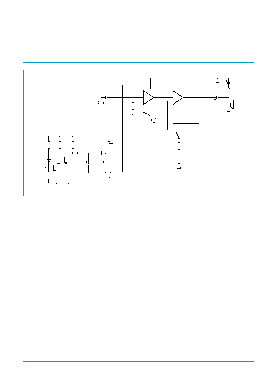
The TFA9841J contains one audio power amplifier. The TFA9841J can be used as
one Single-Ended (SE) channel with a fixed gain of 26 dB.
The TFA9841J comes in a 9-pin DIL-bent-SIL (DBS9P) power package. The
TFA9841J is pin compatible with the TFA9842J and TFA9843J.
The TFA9841J contains a unique protection circuit that is solely based on multiple
temperature measurements inside the chip. This gives maximum output power for all
supply voltages and load conditions with no unnecessary audio holes. Almost any
supply voltage and load impedance combination can be made as long as thermal
boundary conditions (external heatsink and ambient temperature) allow it.
2.
Features
s
SE: 1 W to 7.5 W (into 4
), up to 9 W into (into 8
)
s
Soft clipping
s
Standby and mute mode
s
No on/off switching plops
s
Low standby current
s
High supply voltage ripple rejection
s
Outputs short-circuit protected to ground, supply and across the load
s
Thermally protected
s
Pin compatible with the TFA9842J and TFA9843J.
3.
Applications
s
Television
s
PC speakers
s
Boom box
s
Mini and micro audio receivers.
Philips Semiconductors
TFA9841J
1-channel audio amplifier (1 x SE)
Preliminary data
Rev. 01 -- 06 February 2004
2 of 17
9397 750 12014
� Koninklijke Philips Electronics N.V. 2004. All rights reserved.
4.
Quick reference data
5.
Ordering information
6.
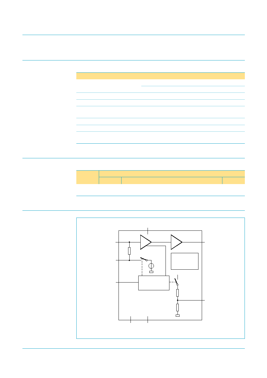
Block diagram
Table 1:
Quick reference data
Symbol Parameter
Conditions
Min
Typ
Max
Unit
V
CC
supply voltage
operating
9
17
26
V
no signal
-
-
28
V
I
q
quiescent supply current V
CC
= 18 V; R
L
=
-
60
100
mA
I
stb
standby supply current
-
-
10
�
A
P
o
output power
V
CC
= 17 V; R
L
= 4
;
THD = 10 %
7
7.5
-
W
THD
total harmonic distortion
P
o
= 1 W
-
0.1
0.5
%
G
v
voltage gain
25
26
27
dB
SVRR
supply voltage ripple
rejection
f = 1 kHz
-
60
-
dB
Table 2:
Ordering information
Type
number
Package
Name
Description
Version
TFA9841J
DBS9P
plastic DIL-bent-SIL power package; 9 leads
(lead length 12/11 mm); exposed die pad
SOT523 -1
Fig 1.
Block diagram.
MDB795
STANDBY
MUTE
ON
SHORT-CIRCUIT
AND
TEMPERATURE
PROTECTION
VREF
0.5VCC
VCC
VCC
9
IN1
-
OUT1
-
SVR
CIV
MODE
3
1
7
2
6
5
GND
4, 8
n.c.
TFA9841J
Philips Semiconductors
TFA9841J
1-channel audio amplifier (1 x SE)
Preliminary data
Rev. 01 -- 06 February 2004
3 of 17
9397 750 12014
� Koninklijke Philips Electronics N.V. 2004. All rights reserved.
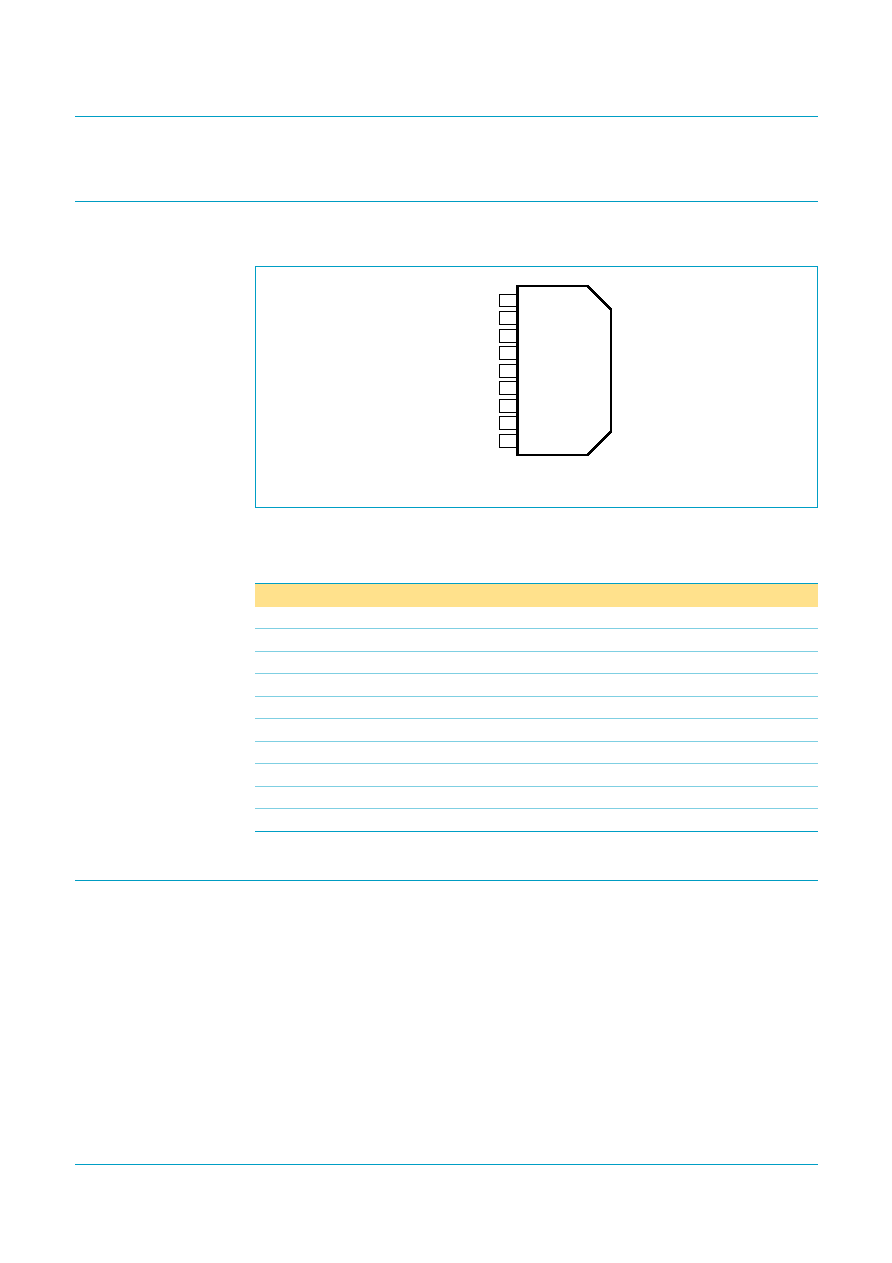
7.
Pinning information
7.1 Pinning
7.2 Pin description
8.
Functional description
8.1 Input configuration
The input cut-off frequency is:
(1)
SE application: R
i
= 60 k
and C
i
= 220 nF:
(2)
Fig 2.
Pin configuration.
TFA9841J
MDB796
IN1
-
OUT1
-
CIV
n.c.
GND
SVR
MODE
n.c.
VCC
2
1
3
4
5
6
7
8
9
Table 3:
Pin description
Symbol
Pin
Description
IN1
-
1
input 1
OUT1
-
2
inverted loudspeaker terminal 1
CIV
3
common input voltage decoupling
n.c.
4
not connected
GND
5
ground
SVR
6
half supply voltage decoupling (ripple rejection)
MODE
7
mode selection input (standby, mute and operating)
n.c.
8
not connected
V
CC
9
supply voltage
TAB
-
back side tab or heats spreader has to be connected to ground
f
i cut
off
�
(
)
1
2
R
i
C
i
�
(
)
-----------------------------
=
f
i cut
off
�
(
)
1
2
60
10
3
�
220
�
10
9
�
�
(
)
-----------------------------------------------------------------
12 Hz
=
=

Philips Semiconductors
TFA9841J
1-channel audio amplifier (1 x SE)
Preliminary data
Rev. 01 -- 06 February 2004
4 of 17
9397 750 12014
� Koninklijke Philips Electronics N.V. 2004. All rights reserved.
As shown in
Equation 2
, large capacitor values for the inputs are not necessary, so
the switch-on delay during charging of the input capacitors can be minimized. This
results in a good low frequency response and good switch-on behavior.
8.2 Power amplifier
The power amplifier is a Single-Ended (SE) amplifier with an all-NPN output stage,
capable of delivering a peak output current of 3 A.
8.2.1
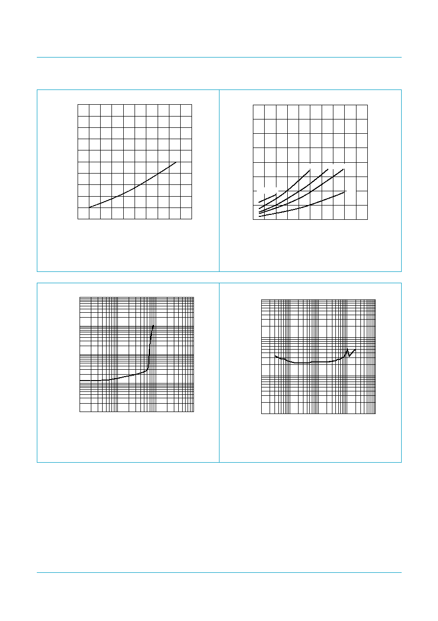
Output power measurement
The output power as a function of the supply voltage is measured on the output pins
at THD = 10 %; see
Figure 5
.
The maximum output power is limited by the supply voltage of 26 V and the maximum
available output current is 3 A (repetitive peak current).
A minimum load of 4
is required for V
CC
> 22 V; see
Figure 6
8.2.2
Headroom
Typical CD music requires at least 12 dB (factor 15.85) dynamic headroom,
compared to the average power output, for transferring the loudest parts without
distortion. At V
CC
= 18 V and P
o
= 5 W (R
L
= 4
) at THD = 0.2 % (see
Figure 7
), the
Average Listening Level (ALL) music power without any distortion yields:
(3)
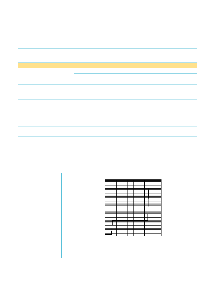
The power dissipation can be derived from
Figure 9
for a headroom of 0 dB and
12 dB, respectively (see
Table 4
).
For the average listening level a power dissipation of 2.2 W can be used for a
heatsink calculation.
8.3 Mode selection
The TFA9841J has three functional modes, which can be selected by applying the
proper DC voltage to pin MODE (see
Table 5
and
Figure 3
).
Table 4:
Power rating as function of headroom
Headroom
Power output (THD = 0.2 %)
Power dissipation
0 dB
P
o
= 5 W
P
D
= 4.4 W
12 dB
P
o(ALL)
= 315 mW
P
D
= 2.2 W
P
o ALL
(
)
5 10
3
15.85
---------------
315 mW
=
=
Table 5:
Mode selection
V
MODE
Amplifier
0 to 0.8 V
standby
4.5 V to (V
CC
-
3.5 V)
mute
(V
CC
-
2.0 V) to V
CC
on
Philips Semiconductors
TFA9841J
1-channel audio amplifier (1 x SE)
Preliminary data
Rev. 01 -- 06 February 2004
5 of 17
9397 750 12014
� Koninklijke Philips Electronics N.V. 2004. All rights reserved.
Standby -- The current consumption is very low and the output is floating. The
device is in standby mode when V
MODE
< 0.8 V, or when pin MODE is grounded.
Mute -- The amplifier is DC-biased but not operational (no audio output). This allows
the input coupling capacitors to be charged to avoid pop-noise. The device is in mute
mode when 4.5 V < V
MODE
< (V
CC
-
3.5 V).
On -- The amplifier is operating normally. The operating mode is activated at
V
MODE
> (V
CC
-
2.0 V).
8.4 Supply voltage ripple rejection
The supply voltage ripple rejection (SVRR) is measured with an electrolytic capacitor
of 150
�
F on pin SVR using a bandwidth of 20 Hz to 22 kHz.
Figure 10
illustrates the
SVRR as function of the frequency. A larger capacitor value on pin SVR improves the
ripple rejection behavior at the lower frequencies.
8.5 Built-in protection circuits
The TFA9841J contains two types of temperature sensors; one measures local
temperatures of the power stage and one measures the global chip temperature. At a
local temperature of the power stage of approximately 185
o
C or a global temperature
of approximately 150
o
C, this detection circuit switches off the power stage for 2 ms.
High impedance of the output is the result. After this time period, the power stage
switches on automatically and the detection will take place again; still a too high
temperature switches off the power stage immediately. This protects the TFA9841J
against shorts to ground, to the supply voltage, across the load and too high chip
temperatures.
The protection will only be activated when necessary, so even during a short-circuit
condition, a certain amount of (pulsed) current will still be flowing through the short,
just as much as the power stage can handle without exceeding the critical
temperature level.
Fig 3.
Mode selection.
MDB797
standby
mute
on
0.8
4.5
VCC
-
3.5
VCC
VMODE (V)
VCC
-
2.0

Philips Semiconductors
TFA9841J
1-channel audio amplifier (1 x SE)
Preliminary data
Rev. 01 -- 06 February 2004
6 of 17
9397 750 12014
� Koninklijke Philips Electronics N.V. 2004. All rights reserved.
9.
Limiting values
10. Thermal characteristics
11. Static characteristics
[1]
A minimum load of 4
is required at V
CC
> 22 V.
[2]
With a load connected at the outputs the quiescent supply current will increase.
[3]
The DC output voltage with respect to ground is approximately 0.5V
CC
.
Table 6:
Limiting values
In accordance with the Absolute Maximum Rating System (IEC 60134).
Symbol
Parameter
Conditions
Min
Max
Unit
V
CC
supply voltage
operating
-
0.3
+26
V
no signal
-
0.3
+28
V
V
I
input voltage
-
0.3
V
CC
+ 0.3
V
I
ORM
repetitive peak output current
-
3
A
T
stg
storage temperature
non-operating
-
55
+150
�
C
T
amb
ambient temperature
operating
-
40
+85
�
C
P
tot
total power dissipation
-
8
W
V
CC(sc)
supply voltage to guarantee short-circuit
protection
-
24
V
Table 7:
Thermal characteristics
Symbol
Parameter
Conditions
Value
Unit
R
th(j-a)
thermal resistance from junction to ambient
in free air
40
K/W
R
th(j-c)
thermal resistance from junction to case
channel driven
4.0
K/W
Table 8:
Static characteristics
V
CC
= 17 V; T
amb
= 25
�
C; R
L
= 4
; V
MODE
= V
CC
; V
i
= 0 V; measured in test circuit
Figure 11
; unless otherwise specified.
Symbol
Parameter
Conditions
Min
Typ
Max
Unit
V
CC
supply voltage
operating
[1]
9
17
26
V
I
q
quiescent supply current
R
L
=
[2]
-
60
100
mA
I
stb
standby supply current
V
MODE
= 0
-
-
10
�
A
V
O
DC output voltage
[3]
-
9
-
V
V
MODE
mode selection input voltage
on mode
V
CC
-
2.0
-
V
CC
V
mute mode
4.5
-
V
CC
-
3.5
V
standby mode
0
-
0.8
V
I
MODE
input current on pin MODE
0 < V
MODE
< V
CC
-
3.5
-
-
20
�
A
Philips Semiconductors
TFA9841J
1-channel audio amplifier (1 x SE)
Preliminary data
Rev. 01 -- 06 February 2004
7 of 17
9397 750 12014
� Koninklijke Philips Electronics N.V. 2004. All rights reserved.
12. Dynamic characteristics
[1]
The noise output voltage is measured at the output in a frequency range from 20 Hz to 22 kHz (unweighted), with a source impedance
R
source
= 0
at the input.
[2]
Supply voltage ripple rejection is measured at the output, with a source impedance R
source
= 0
at the input and with a frequency range
from 20 Hz to 22 kHz (unweighted). The ripple voltage is a sine wave with a frequency f
ripple
and an amplitude of 300 mV (RMS), which
is applied to the positive supply rail.
[3]
Output voltage in mute mode (V
MODE
= 7 V) is measured with an input voltage of 1 V (RMS) in a bandwidth from 20 Hz to 22 kHz,
including noise.
Table 9:
Dynamic characteristics
V
CC
= 17 V; T
amb
= 25
�
C; R
L
= 4
; f = 1 kHz; V
MODE
= V
CC
; measured in test circuit
Figure 11
; unless otherwise specified.
Symbol
Parameter
Conditions
Min
Typ
Max
Unit
P
o
output power
R
L
= 4
; see
Figure 6
THD = 10 %
-
7.5
-
W
THD = 0.5 %
-
6.1
-
W
THD
total harmonic distortion
P
o
= 1 W; see
Figure 7
and
Figure 8
-
0.1
0.5
%
G
v
SE voltage gain
25
26
27
dB
Z
i
input impedance
40
60
-
k
V
n(o)
noise output voltage
[1]
-
150
-
�
V
SVRR
supply voltage ripple
rejection
see
Figure 10
f
ripple
= 1 kHz
[2]
-
60
-
dB
f
ripple
= 100 Hz to 20 kHz
[2]
-
60
-
dB
V
o(mute)
output voltage in mute
mode
[3]
-
-
150
�
V
V
i
= 50 mV; V
CC
= 18 V.
Fig 4.
AC output voltage as function of mode selection voltage.
20
VMODE (V)
0
4
8
12
Vo
(
�
V)
16
10
7
10
6
10
5
10
4
10
3
10
2
10
1
MDB798
Philips Semiconductors
TFA9841J
1-channel audio amplifier (1 x SE)
Preliminary data
Rev. 01 -- 06 February 2004
8 of 17
9397 750 12014
� Koninklijke Philips Electronics N.V. 2004. All rights reserved.
THD = 10 %; R
L
= 4
; f = 1 kHz.
THD = 10 %.
Fig 5.
Output power as function of supply voltage.
Fig 6.
Output power as function of supply voltage for
various SE loads.
Po
(W)
8
14
10
16
18
VCC (V)
12
0
15
9
12
3
6
MDB809
P
o
(W)
8
20
12
24
28
V
CC
(V)
16
0
40
30
10
20
mdb806
2
3
4
8
R
L
= 1
V
CC
= 18 V; f = 1 kHz; R
L
= 4
.
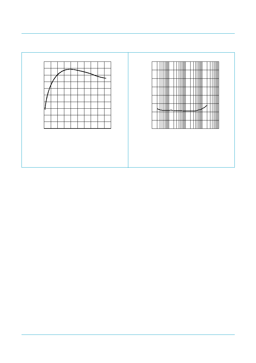
V
CC
= 17 V; P
o
= 1 W; R
L
= 4
.
Fig 7.
Total harmonic distortion-plus-noise as
function of output power.
Fig 8.
Total harmonic distortion-plus-noise as
function of frequency.
10
2
10
1
10
-
1
10
-
2
MCE488
10
-
1
10
2
1
10
Po (W)
THD
+
N
(%)
10
1
10
-
1
10
-
2
MCE489
10
THD
+
N
(%)
f (Hz)
10
2
10
3
10
4
10
5
Philips Semiconductors
TFA9841J
1-channel audio amplifier (1 x SE)
Preliminary data
Rev. 01 -- 06 February 2004
9 of 17
9397 750 12014
� Koninklijke Philips Electronics N.V. 2004. All rights reserved.
V
CC
= 18 V; R
L
= 4
.
V
CC
= 17 V; R
source
= 0
; V
ripple
= 300 mV (RMS); a
bandpass filter of 20 Hz to 22 kHz has been applied
input short-circuited.
Fig 9.
Total power dissipation as function of channel
output power.
Fig 10. Supply voltage ripple rejection as function of
frequency.
0
10
Po (W)
5
0
1
2
3
4
2
PD
(W)
4
6
8
MDB799
-
80
-
60
-
40
-
20
0
MCE497
10
SVRR
(dB)
f (Hz)
10
2
10
3
10
4
10
5
Philips Semiconductors
TFA9841J
1-channel audio amplifier (1 x SE)
Preliminary data
Rev. 01 -- 06 February 2004
10 of 17
9397 750 12014
� Koninklijke Philips Electronics N.V. 2004. All rights reserved.
13. Application information
Remark: Because of switching inductive loads, the output voltage can rise beyond
the maximum supply voltage of 28 V. At high supply voltages, it is recommended to
use (Schottky) diodes to the supply voltage and ground.
13.1 Printed-circuit board
13.1.1
Layout and grounding
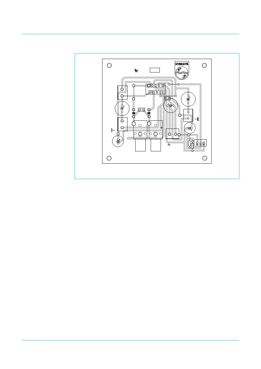
To obtain a high-level system performance, certain grounding techniques are
essential. The input reference grounds have to be tied with their respective source
grounds and must have separate tracks from the power ground tracks; this will
prevent the large (output) signal currents from interfering with the small AC input
signals. The small-signal ground tracks should be physically located as far as
possible from the power ground tracks. Supply and output tracks should be as wide
as possible for delivering maximum output power.
Fig 11. Typical SE application diagram.
mdb794
STANDBY
MUTE
ON
SHORT-CIRCUIT
AND
TEMPERATURE
PROTECTION
V
REF
V
CC
V
CC
9
IN1
-
OUT1
-
CIV
MODE
1
3
7
2
TFA9841J
220 nF
Vi
V
CC
1000
�
F
470
�
F
100 nF
R
L
4
+
-
0.5V
CC
SVR 6
5
GND
V
CC
2.2
�
F
10
k
50
k
270
BC547
BC547
7.5 V
micro-
controller
47
�
F
22
�
F
1.5
k
100
k
Philips Semiconductors
TFA9841J
1-channel audio amplifier (1 x SE)
Preliminary data
Rev. 01 -- 06 February 2004
11 of 17
9397 750 12014
� Koninklijke Philips Electronics N.V. 2004. All rights reserved.
13.1.2
Power supply decoupling
Proper supply bypassing is critical for low-noise performance and high supply voltage
ripple rejection. The respective capacitor location should be as close as possible to
the device and grounded to the power ground. Proper power supply decoupling also
prevents oscillations.
For suppressing higher frequency transients (spikes) on the supply line a capacitor
with low ESR, typical 100 nF, has to be placed as close as possible to the device. For
suppressing lower frequency noise and ripple signals, a large electrolytic capacitor,
e.g. 1000
�
F or greater, must be placed close to the device.
The bypass capacitor on pin SVR reduces the noise and ripple on the mid rail
voltage. For good THD and noise performance a low ESR capacitor is recommended.
13.2 Thermal behavior and heatsink calculation
The measured maximum thermal resistance of the IC package, R
th(j-mb)
, is 4.0 K/W.
A calculation for the heatsink can be made, with the following parameters:
T
amb(max)
= 60
�
C (example)
V
CC
= 18 V and R
L
= 4
T
j(max)
= 150
�
C (specification)
R
th(tot)
is the total thermal resistance between the junction and the ambient including
the heatsink. This can be calculated using the maximum temperature increase
divided by the power dissipation:
R
th(tot)
= (T
j(max)
-
T
amb(max)
)/P
D
Fig 12. Printed-circuit board layout (single-sided); components view.
AUDIO POWER CS NIJMEGEN
27 Jan.
2003 / FP
IN2
+
IN1
+
MUTE
SB ON
TVA
TFA9843J
-
SE2
+
-
SE1
+
+VP
1000
�
F
1000
�
F
1000
�
F
BTL1/2
1
22
�
F
10 k
10
k
MCE506
100 nF
150
�
F
220
nF
220
nF
MODE
SGND
SVR
SVR
CIV
CIV
Philips Semiconductors
TFA9841J
1-channel audio amplifier (1 x SE)
Preliminary data
Rev. 01 -- 06 February 2004
12 of 17
9397 750 12014
� Koninklijke Philips Electronics N.V. 2004. All rights reserved.
At V
CC
= 18 V and R
L
= 4
the measured worst-case sine-wave dissipation is 4.4 W;
see
Figure 9
.
For T
j(max)
= 150
�
C the temperature raise, caused by the power dissipation, is:
150
-
60 = 90
�
C:
P
�
R
th(tot)
= 90
�
C
R
th(tot)
= 90/4.4 = 20.5 K/W
R
th(h-a)
= R
th(tot)
-
R
th(j-mb)
= 20.5
-
4.0 = 16.5 K/W.
This calculation is for an application at worst-case sine-wave output signals. In
practice music signals will be applied, which decreases the maximum power
dissipation to approximately half of the sine-wave power dissipation (see
Section 8.2.2
). This allows for the use of a smaller heatsink:
P
�
R
th(tot)
= 90
�
C
R
th(tot)
= 90/2.2 = 40.9 K/W
R
th(h-a)
= R
th(tot)
-
R
th(j-mb)
= 40.9
-
4.0 = 36.9 K/W.
14. Test information
14.1 Quality information
The
General Quality Specification for Integrated Circuits, SNW-FQ-611 is applicable.
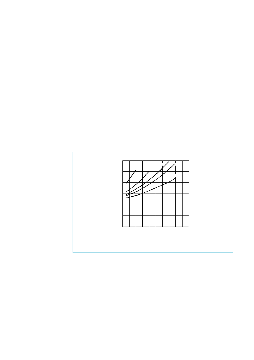
External heatsink of 10 K/W; with music signals; T
amb
= 25
�
C.
Fig 13. Junction temperature as function of supply voltage for various loads.
8
150
100
50
0
12
28
VCC (V)
16
20
24
MDB800
Tj
(
�
C)
2
RL = 1
3
4
8
Philips Semiconductors
TFA9841J
1-channel audio amplifier (1 x SE)
Preliminary data
Rev. 01 -- 06 February 2004
13 of 17
9397 750 12014
� Koninklijke Philips Electronics N.V. 2004. All rights reserved.
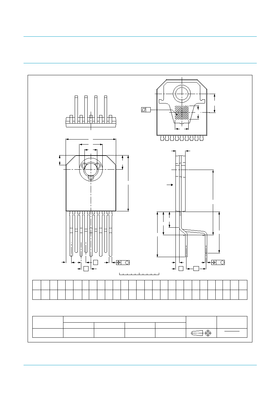
15. Package outline
Fig 14. DBS9P package outline.
REFERENCES
OUTLINE
VERSION
EUROPEAN
PROJECTION
ISSUE DATE
IEC
JEDEC
JEITA
DIMENSIONS (mm are the original dimensions)
Notes
1. Plastic or metal protrusions of 0.25 mm maximum per side are not included.
2. Plastic surface within circle area D1 may protrude 0.04 mm maximum.
SOT523-1
0
10 mm
5
scale
w
M
bp
Dh
q1
Z
1
9
e
e1
m
e2
x
A2
non-concave
D1
D
P
k
q2
L3
L2
L
Q
c
E
00-07-03
03-03-12
DBS9P: plastic DIL-bent-SIL power package; 9 leads (lead length 12/11 mm); exposed die pad
SOT523-1
view B: mounting base side
B
UNIT
bp
L1
c
D
(1)
Dh
L
q2
mm
2.7
2.3
A2
(2)
0.80
0.65
0.58
0.48
13.2
12.8
D1
(2)
6.2
5.8
3.5
Eh
3.5
e
2.54
e1
1.27
e2
5.08
4.85
Q
E
(1)
14.7
14.3
Z
(1)
1.65
1.10
11.4
10.0
L2
6.7
5.5
L3
4.5
3.7
3.4
3.1
1.15
0.85
q
17.5
16.3
q1
2.8
m
0.8
v
3.8
3.6
3
2
12.4
11.0
P
k
0.02
x
0.3
w
Eh
L1
q
v
M

Philips Semiconductors
TFA9841J
1-channel audio amplifier (1 x SE)
Preliminary data
Rev. 01 -- 06 February 2004
14 of 17
9397 750 12014
� Koninklijke Philips Electronics N.V. 2004. All rights reserved.
16. Soldering
16.1 Introduction to soldering through-hole mount packages
This text gives a brief insight to wave, dip and manual soldering. A more in-depth
account of soldering ICs can be found in our
Data Handbook IC26; Integrated Circuit
Packages (document order number 9398 652 90011).
Wave soldering is the preferred method for mounting of through-hole mount IC
packages on a printed-circuit board.
16.2 Soldering by dipping or by solder wave
Driven by legislation and environmental forces the worldwide use of lead-free solder
pastes is increasing. Typical dwell time of the leads in the wave ranges from
3 to 4 seconds at 250
�
C or 265
�
C, depending on solder material applied, SnPb or
Pb-free respectively.
The total contact time of successive solder waves must not exceed 5 seconds.
The device may be mounted up to the seating plane, but the temperature of the
plastic body must not exceed the specified maximum storage temperature (T
stg(max)
).
If the printed-circuit board has been pre-heated, forced cooling may be necessary
immediately after soldering to keep the temperature within the permissible limit.
16.3 Manual soldering
Apply the soldering iron (24 V or less) to the lead(s) of the package, either below the
seating plane or not more than 2 mm above it. If the temperature of the soldering iron
bit is less than 300
�
C it may remain in contact for up to 10 seconds. If the bit
temperature is between 300 and 400
�
C, contact may be up to 5 seconds.
16.4 Package related soldering information
[1]
For SDIP packages, the longitudinal axis must be parallel to the transport direction of the
printed-circuit board.
[2]
For PMFP packages hot bar soldering or manual soldering is suitable.
Table 10:
Suitability of through-hole mount IC packages for dipping and wave
soldering methods
Package
Soldering method
Dipping
Wave
DBS, DIP, HDIP, RDBS, SDIP, SIL
suitable
suitable
[1]
PMFP
[2]
-
not suitable

Philips Semiconductors
TFA9841J
1-channel audio amplifier (1 x SE)
Preliminary data
Rev. 01 -- 06 February 2004
15 of 17
9397 750 12014
� Koninklijke Philips Electronics N.V. 2004. All rights reserved.
17. Revision history
Table 11:
Revision history
Rev Date
CPCN
Description
01
20040206
-
Preliminary data (9397 750 12014)

9397 750 12014
Philips Semiconductors
TFA9841J
1-channel audio amplifier (1 x SE)
� Koninklijke Philips Electronics N.V. 2004. All rights reserved.
Preliminary data
Rev. 01 -- 06 February 2004
16 of 17
Contact information
For additional information, please visit http://www.semiconductors.philips.com.
For sales office addresses, send e-mail to: sales.addresses@www.semiconductors.philips.com.
Fax: +31 40 27 24825
18. Data sheet status
[1]
Please consult the most recently issued data sheet before initiating or completing a design.
[2]
The product status of the device(s) described in this data sheet may have changed since this data sheet was published. The latest information is available on the Internet at
URL http://www.semiconductors.philips.com.
[3]
For data sheets describing multiple type numbers, the highest-level product status determines the data sheet status.
19. Definitions
Short-form specification -- The data in a short-form specification is
extracted from a full data sheet with the same type number and title. For
detailed information see the relevant data sheet or data handbook.
Limiting values definition -- Limiting values given are in accordance with
the Absolute Maximum Rating System (IEC 60134). Stress above one or
more of the limiting values may cause permanent damage to the device.
These are stress ratings only and operation of the device at these or at any
other conditions above those given in the Characteristics sections of the
specification is not implied. Exposure to limiting values for extended periods
may affect device reliability.
Application information -- Applications that are described herein for any
of these products are for illustrative purposes only. Philips Semiconductors
make no representation or warranty that such applications will be suitable for
the specified use without further testing or modification.
20. Disclaimers
Life support -- These products are not designed for use in life support
appliances, devices, or systems where malfunction of these products can
reasonably be expected to result in personal injury. Philips Semiconductors
customers using or selling these products for use in such applications do so
at their own risk and agree to fully indemnify Philips Semiconductors for any
damages resulting from such application.
Right to make changes -- Philips Semiconductors reserves the right to
make changes in the products - including circuits, standard cells, and/or
software - described or contained herein in order to improve design and/or
performance. When the product is in full production (status `Production'),
relevant changes will be communicated via a Customer Product/Process
Change Notification (CPCN). Philips Semiconductors assumes no
responsibility or liability for the use of any of these products, conveys no
licence or title under any patent, copyright, or mask work right to these
products, and makes no representations or warranties that these products are
free from patent, copyright, or mask work right infringement, unless otherwise
specified.
Level
Data sheet status
[1]
Product status
[2][3]
Definition
I
Objective data
Development
This data sheet contains data from the objective specification for product development. Philips
Semiconductors reserves the right to change the specification in any manner without notice.
II
Preliminary data
Qualification
This data sheet contains data from the preliminary specification. Supplementary data will be published
at a later date. Philips Semiconductors reserves the right to change the specification without notice, in
order to improve the design and supply the best possible product.
III
Product data
Production
This data sheet contains data from the product specification. Philips Semiconductors reserves the
right to make changes at any time in order to improve the design, manufacturing and supply. Relevant
changes will be communicated via a Customer Product/Process Change Notification (CPCN).

� Koninklijke Philips Electronics N.V. 2004.
Printed in The Netherlands
All rights are reserved. Reproduction in whole or in part is prohibited without the prior
written consent of the copyright owner.
The information presented in this document does not form part of any quotation or
contract, is believed to be accurate and reliable and may be changed without notice. No
liability will be accepted by the publisher for any consequence of its use. Publication
thereof does not convey nor imply any license under patent- or other industrial or
intellectual property rights.
Date of release: 06 February 2004
Document order number: 9397 750 12014
Contents
Philips Semiconductors
TFA9841J
1-channel audio amplifier (1 x SE)
1
General description . . . . . . . . . . . . . . . . . . . . . . 1
2
Features . . . . . . . . . . . . . . . . . . . . . . . . . . . . . . . 1
3
Applications . . . . . . . . . . . . . . . . . . . . . . . . . . . . 1
4
Quick reference data . . . . . . . . . . . . . . . . . . . . . 2
5
Ordering information . . . . . . . . . . . . . . . . . . . . . 2
6
Block diagram . . . . . . . . . . . . . . . . . . . . . . . . . . 2
7
Pinning information . . . . . . . . . . . . . . . . . . . . . . 3
7.1
Pinning . . . . . . . . . . . . . . . . . . . . . . . . . . . . . . . 3
7.2
Pin description . . . . . . . . . . . . . . . . . . . . . . . . . 3
8
Functional description . . . . . . . . . . . . . . . . . . . 3
8.1
Input configuration . . . . . . . . . . . . . . . . . . . . . . 3
8.2
Power amplifier . . . . . . . . . . . . . . . . . . . . . . . . . 4
8.2.1
Output power measurement . . . . . . . . . . . . . . . 4
8.2.2
Headroom . . . . . . . . . . . . . . . . . . . . . . . . . . . . . 4
8.3
Mode selection . . . . . . . . . . . . . . . . . . . . . . . . . 4
8.4
Supply voltage ripple rejection . . . . . . . . . . . . . 5
8.5
Built-in protection circuits . . . . . . . . . . . . . . . . . 5
9
Limiting values. . . . . . . . . . . . . . . . . . . . . . . . . . 6
10
Thermal characteristics. . . . . . . . . . . . . . . . . . . 6
11
Static characteristics. . . . . . . . . . . . . . . . . . . . . 6
12
Dynamic characteristics . . . . . . . . . . . . . . . . . . 7
13
Application information. . . . . . . . . . . . . . . . . . 10
13.1
Printed-circuit board . . . . . . . . . . . . . . . . . . . . 10
13.1.1
Layout and grounding . . . . . . . . . . . . . . . . . . . 10
13.1.2
Power supply decoupling . . . . . . . . . . . . . . . . 11
13.2
Thermal behavior and heatsink calculation . . 11
14
Test information . . . . . . . . . . . . . . . . . . . . . . . . 12
14.1
Quality information . . . . . . . . . . . . . . . . . . . . . 12
15
Package outline . . . . . . . . . . . . . . . . . . . . . . . . 13
16
Soldering . . . . . . . . . . . . . . . . . . . . . . . . . . . . . 14
16.1
Introduction to soldering through-hole
mount packages . . . . . . . . . . . . . . . . . . . . . . 14
16.2
Soldering by dipping or by solder wave . . . . . 14
16.3
Manual soldering . . . . . . . . . . . . . . . . . . . . . . 14
16.4
Package related soldering information . . . . . . 14
17
Revision history . . . . . . . . . . . . . . . . . . . . . . . . 15
18
Data sheet status . . . . . . . . . . . . . . . . . . . . . . . 16
19
Definitions . . . . . . . . . . . . . . . . . . . . . . . . . . . . 16
20
Disclaimers . . . . . . . . . . . . . . . . . . . . . . . . . . . . 16