 | –≠–ª–µ–∫—Ç—Ä–æ–Ω–Ω—ã–π –∫–æ–º–ø–æ–Ω–µ–Ω—Ç: TZA3005H | –°–∫–∞—á–∞—Ç—å:  PDF PDF  ZIP ZIP |

DATA SHEET
Product specification
Supersedes data of 1997 Aug 05
File under Integrated Circuits, IC19
2000 Feb 17
INTEGRATED CIRCUITS
TZA3005H
SDH/SONET STM1/OC3 and
STM4/OC12 transceiver

2000 Feb 17
2
Philips Semiconductors
Product specification
SDH/SONET STM1/OC3 and STM4/OC12
transceiver
TZA3005H
FEATURES
∑
Supports STM1/OC3 (155.52 Mbits/s) and STM4/OC12
(622.08 Mbits/s)
∑
Supports reference clock frequencies of 19.44, 38.88,
51.84 and 77.76 MHz
∑
Meets Bellcore, ANSI and ITU-T specifications
∑
Meets ITU jitter specification typically to a factor of 2.5
∑
Integral high-frequency PLL for clock generation
∑
Interface to TTL logic
∑
Low jitter PECL (Positive Emitter Coupled Logic)
interface
∑
4 or 8-bit STM1/OC3 TTL data path
∑
4 or 8-bit STM4/OC12 TTL data path
∑
No external filter components required
∑
QFP64 package
∑
Diagnostic and line loopback modes
∑
Lock detect
∑
LOS (Loss of Signal) input
∑
Low power (0.9 W typical)
∑
Selectable frame detection and byte realignment
∑
Loop timing
∑
Forward and reverse clocking
∑
Squelched clock operation
∑
Self-biased PECL inputs to support AC coupling.
APPLICATIONS
∑
SDH/SONET modules
∑
SDH/SONET-based transmission systems
∑
SDH/SONET test equipment
∑
ATM (Asynchronous Transfer Mode) over SDH/SONET
∑
Add drop multiplexers
∑
Broadband cross-connects
∑
Section repeaters
∑
Fibre optic test equipment
∑
Fibre optic terminators.
GENERAL DESCRIPTION
The TZA3005H SDH/SONET transceiver chip is a fully
integrated serialization/deserialization STM1/OC3
(155.52 Mbits/s) and STM4/OC12 (622.08 Mbits/s)
interface device. It performs all necessary serial-to-parallel
and parallel-to-serial functions in accordance with
SDH/SONET transmission standards. It is suitable for
SONET-based applications and can be used in
conjunction with the data and clock recovery unit
(TZA3004), optical front-end (TZA3023 with TZA3034/44)
and a laser driver (TZA3001). A typical network application
is shown in Fig.10.
A high-frequency phase-locked loop is used for on-chip
clock synthesis, which allows a slower external transmit
reference clock to be used. A reference clock of 19.44,
38.88, 51.84 or 77.76 MHz can be used to support existing
system clocking schemes. The TZA3005H also performs
SDH/SONET frame detection.
The low jitter PECL interface ensures that Bellcore, ANSI,
and ITU-T bit-error rate requirements are satisfied.
The TZA3005H is supplied in a compact QFP64 package.
ORDERING INFORMATION
TYPE
NUMBER
PACKAGE
NAME
DESCRIPTION
VERSION
TZA3005H
QFP64
plastic quad flat package; 64 leads (lead length 1.6 mm);
body 14
◊
14
◊
2.7 mm
SOT393-1
2000 Feb 17
3
Philips Semiconductors
Product specification
SDH/SONET STM1/OC3 and STM4/OC12
transceiver
TZA3005H
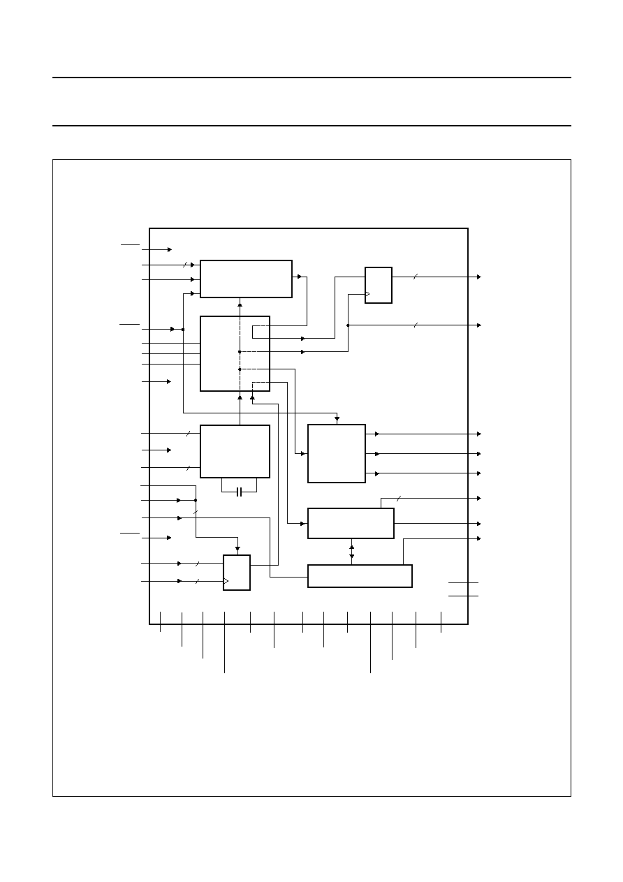
BLOCK DIAGRAM
handbook, full pagewidth
CLOCK
DIVIDER
BY 4 OR BY 8
CLOCK
SYNTHESIZER
RF
SWITCH
BOX
(1)
1:8 OR 1:4
SERIAL TO PARALLEL
8:1 OR 4:1
PARALLEL TO SERIAL
on-chip capacitor
RECEIVER
TZA3005H
TRANSMITTER
FRAME HEADER DETECT
D
D
LLEN
31
53 to 60
61
TXPCLK
TXPD0 to
TXPD7
8
2
2
2
8
2
2
REFSEL0 and
REFSEL1
REFCLK and
REFCLKQ
MRST
TEST1
MODE
BUSWIDTH
3, 4
2
RXSD and
RXSDQ
24, 25
2
RXSCLK and
RXSCLKQ
27, 28
48
10
TEST2
11
TEST3
13
49
SDTTL
22
SDPECL
23
OOF
33
15, 14
30
DLEN
32
17, 18
21, 20
62
63
64
36, 37, 39, 40,
41, 43 to 45
47
35
TXSD and
TXSDQ
TXSCLK and
TXSCLKQ
SYNCLKDIV
LOCKDET
RXPD0 to
RXPD7
19MHZO
RXPCLK
FP
VCC(TXCORE)
52
GNDTXCORE
51
MGS975
1
VCC(SYNOUT)
VCCD(SYN)
VCCA(SYN) VCC(TXOUT)
VCC(RXCORE)
VCC(RXOUT)
GNDRXOUT
DGNDSYN
AGNDSYN
GNDSYNOUT
GNDTXOUT
GNDRXCORE
2
5
8, 9
6
7
16
19
26
29
38, 46
GND
12
34, 42
Fig.1 Block diagram.
(1) Dashed lines represent normal operation mode.

2000 Feb 17
4
Philips Semiconductors
Product specification
SDH/SONET STM1/OC3 and STM4/OC12
transceiver
TZA3005H
PINNING
SYMBOL
PIN
TYPE
(1)
DESCRIPTION
V
CC(SYNOUT)
1
S
supply voltage (synthesizer output)
GND
SYNOUT
2
G
ground (synthesizer output)
REFSEL0
3
I
reference clock select input 0
REFSEL1
4
I
reference clock select input 1
DGND
SYN
5
G
digital ground (synthesizer)
V
CCD(SYN)
6
S
digital supply voltage (synthesizer)
V
CCA(SYN)
7
S
analog supply voltage (synthesizer)
AGND
SYN
8
G
analog ground (synthesizer)
AGND
SYN
9
G
analog ground (synthesizer)
TEST1
10
I
test and control input
TEST2
11
I
test and control input
GND
12
G
ground
TEST3
13
I
test and control input
REFCLKQ
14
I
inverted reference clock input
REFCLK
15
I
reference clock input
V
CC(TXOUT)
16
S
supply voltage (transmitter output)
TXSD
17
O
serial data output
TXSDQ
18
O
inverted serial data output
GND
TXOUT
19
G
ground (transmitter output)
TXSCLKQ
20
O
inverted serial clock output
TXSCLK
21
O
serial clock output
SDTTL
22
I
TTL signal detect input
SDPECL
23
I
PECL signal detect input
RXSD
24
I
serial data input
RXSDQ
25
I
inverted serial data input
V
CC(RXCORE)
26
S
supply voltage (receiver core)
RXSCLK
27
I
serial clock input
RXSCLKQ
28
I
inverted serial clock input
GND
RXCORE
29
G
ground (receiver core)
BUSWIDTH
30
I
4/8 bus width select input
LLEN
31
I
line loopback enable input (active LOW)
DLEN
32
I
diagnostic loopback enable input (active LOW)
OOF
33
I
out-of-frame enable input
GND
RXOUT
34
G
ground (receiver output)
FP
35
O
frame pulse output
RXPD0
36
O
parallel data output 0
RXPD1
37
O
parallel data output 1
V
CC(RXOUT)
38
S
supply voltage (receiver output)
RXPD2
39
O
parallel data output 2
RXPD3
40
O
parallel data output 3

2000 Feb 17
5
Philips Semiconductors
Product specification
SDH/SONET STM1/OC3 and STM4/OC12
transceiver
TZA3005H
Note
1. Pin type abbreviations: O = Output, I = Input, S = Supply, G = Ground.
RXPD4
41
O
parallel data output 4
GND
RXOUT
42
G
ground (receiver output)
RXPD5
43
O
parallel data output 5
RXPD6
44
O
parallel data output 6
RXPD7
45
O
parallel data output 7
V
CC(RXOUT)
46
S
supply voltage (receiver output)
RXPCLK
47
O
receive parallel clock output
MRST
48
I
master reset (active LOW)
MODE
49
I
serial data rate select STM1/STM4
ALTPIN
50
I
test and control input
GND
TXCORE
51
G
ground (transmitter core)
V
CC(TXCORE)
52
S
supply voltage (transmitter core)
TXPD0
53
I
parallel data input 0
TXPD1
54
I
parallel data input 1
TXPD2
55
I
parallel data input 2
TXPD3
56
I
parallel data input 3
TXPD4
57
I
parallel data input 4
TXPD5
58
I
parallel data input 5
TXPD6
59
I
parallel data input 6
TXPD7
60
I
parallel data input 7
TXPCLK
61
I
transmit parallel clock input
SYNCLKDIV
62
O
transmit byte/nibble clock output (synchronous)
LOCKDET
63
O
lock detect output
19MHZO
64
O
19 MHz reference clock output
SYMBOL
PIN
TYPE
(1)
DESCRIPTION