 | –≠–ª–µ–∫—Ç—Ä–æ–Ω–Ω—ã–π –∫–æ–º–ø–æ–Ω–µ–Ω—Ç: TZA3013B | –°–∫–∞—á–∞—Ç—å:  PDF PDF  ZIP ZIP |
Document Outline
- FEATURES
- APPLICATIONS
- GENERAL DESCRIPTION
- ORDERING INFORMATION
- BLOCK DIAGRAM
- PINNING
- FUNCTIONAL DESCRIPTION
- PIN diode bias voltage DREF
- AGC
- LIMITING VALUES
- HANDLING
- CHARACTERISTICS
- TYPICAL PERFORMANCE CHARACTERISTICS
- APPLICATION AND TEST INFORMATION
- BONDING PAD LOCATIONS
- Physical characteristics of the bare die
- DATA SHEET STATUS
- DEFINITIONS
- DISCLAIMERS
- BARE DIE DISCLAIMER

DATA SHEET
Product specification
Supersedes data of 2000 Jun 19
File under Integrated Circuits, IC19
2001 Feb 26
INTEGRATED CIRCUITS
TZA3013A; TZA3013B
SDH/SONET STM16/OC48
transimpedance amplifier

2001 Feb 26
2
Philips Semiconductors
Product specification
SDH/SONET STM16/OC48
transimpedance amplifier
TZA3013A; TZA3013B
FEATURES
∑
Low equivalent input noise, typically 8 pA/
Hz
∑
Wide dynamic range, typically 6
µ
A to 1.7 mA (p-p)
∑
Differential transimpedance of 4 k
∑
Bandwidth from DC to 1.9 GHz
∑
Differential outputs
∑
On-chip Automatic Gain Control (AGC)
∑
No external components required
∑
Single supply voltage 3.3 V
∑
Bias voltage for PIN diode
∑
Remains linear up to 1.7 mA (p-p) input current
(unclipped)
∑
Switched output polarity available (types A and B).
APPLICATIONS
∑
Digital fibre optic receiver in short, medium and long
haul optical telecommunications transmission systems
or in high speed data networks
∑
Wide-band RF gain block.
GENERAL DESCRIPTION
The TZA3013 is a transimpedance amplifier with AGC,
designed to be used in STM16/OC48 fibre-optic links.
It amplifies the current generated by a photo detector
(PIN diode or avalanche photodiode) and converts it to a
differential output voltage.
ORDERING INFORMATION
TYPE
NUMBER
PACKAGE
NAME
DESCRIPTION
VERSION
TZA3013AU
-
bare die in waffle pack carriers; die dimensions 0.810
◊
1.230 mm
-
TZA3013BU
-
bare die in waffle pack carriers; die dimensions 0.810
◊
1.230 mm
-
2001 Feb 26
3
Philips Semiconductors
Product specification
SDH/SONET STM16/OC48
transimpedance amplifier
TZA3013A; TZA3013B
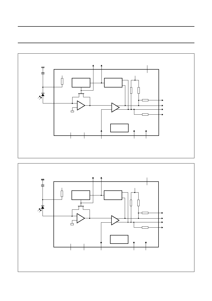
BLOCK DIAGRAM
handbook, full pagewidth
MGT099
2 k
2 k
50
50
3
7, 8
10
270
100 pF
TZA3013AU
GAIN
CONTROL
BIAS
SOURCE
INQ
low noise
amplifier
single-ended to
differential converter
PEAK
DETECTOR
9
15
1
2
DREF
IN
4
12
OUTSENSE
14
OUT
13
OUTQ
6
OUTQSENSE
5
TESTC
GNDA
GNDD
VCC
VCC
VCC
AGC
PILOT
11
TESTD
Fig.1 Block diagram of TZA3013AU (bare die only).
handbook, full pagewidth
MGU137
2 k
2 k
50
50
3
7, 8
10
270
100 pF
TZA3013BU
GAIN
CONTROL
BIAS
SOURCE
INQ
low noise
amplifier
single-ended to
differential converter
PEAK
DETECTOR
9
15
1
2
DREF
IN
4
12
OUTSENSE
5
OUT
6
OUTQ
13
OUTQSENSE
14
TESTC
GNDA
GNDD
VCC
VCC
VCC
AGC
PILOT
11
TESTD
Fig.2 Block diagram of TZA3013BU (bare die only).

2001 Feb 26
4
Philips Semiconductors
Product specification
SDH/SONET STM16/OC48
transimpedance amplifier
TZA3013A; TZA3013B
PINNING
Notes
1. DC bias voltage = 0.86 V.
2. This pad goes HIGH when current flows into pad IN.
SYMBOL
PAD
TZA3013AU
PAD
TZA3013BU
TYPE
DESCRIPTION
DREF
1
1
analog
output
bias voltage output for PIN diode; connect cathode of
PIN diode to this pad
IN
2
2
input
current input; anode of PIN diode should be connected to
this pad; note 1
INQ
3
3
input
decision level adjust input; note 1
AGC
4
4
analog
output
AGC voltage
OUTQSENSE
5
14
analog
output
data sense output for OUTQ; for test purposes
OUTQ
6
13
output
data output; compliment of OUT
GNDA
7
7
ground
analog ground
GNDA
8
8
ground
analog ground
TESTC
9
9
input
test input; not used in the application
GNDD
10
10
ground
digital ground
TESTD
11
11
input
test input; not used in the application
PILOT
12
12
analog
output
pilot tone detection current output
OUT
13
6
output
data output; compliment of OUTQ; note 2
OUTSENSE
14
5
analog
output
data sense output for OUT; for test purposes
V
CC
15
15
supply
supply voltage

2001 Feb 26
5
Philips Semiconductors
Product specification
SDH/SONET STM16/OC48
transimpedance amplifier
TZA3013A; TZA3013B
FUNCTIONAL DESCRIPTION
The TZA3013 is a transimpedance amplifier intended for
use in fibre optic links for signal recovery in STM16/OC48
applications. It amplifies the current generated by a photo
detector (PIN diode or avalanche photodiode) and
converts it to a differential output voltage.
The most important characteristics of the TZA3013 are
high receiver sensitivity and wide dynamic range. High
receiver sensitivity is achieved by minimizing
transimpedance amplifier noise.
The TZA3013 has a wide dynamic range to handle the
signal current generated by the PIN diode which can vary
from 6
µ
A to 1.7 mA (p-p). This is implemented by an AGC
loop which reduces the preamplifier feedback resistance
so that the amplifier remains linear over the whole input
range. The AGC loop hold capacitor is integrated on-chip,
so an external capacitor is not required.
A differential amplifier converts the output of the
preamplifier to a differential voltage. The data output circuit
is shown in Fig.3.
The logic level symbol definitions are shown in Fig.4.
handbook, full pagewidth
MGT102
2 k
2 k
16
OUTSENSE
VCC
OUTQSENSE
OUT
50
16
OUTQ
50
Fig.3 Data output circuit.
handbook, full pagewidth
MGR243
VOO
VO(max)
VOQH
VOH
VOQL
VOL
VO(min)
Vo(p-p)
VCC
Fig.4 Logic level symbol definitions for data outputs OUT and OUTQ.

2001 Feb 26
6
Philips Semiconductors
Product specification
SDH/SONET STM16/OC48
transimpedance amplifier
TZA3013A; TZA3013B
PIN diode bias voltage DREF
The performance of an optical receiver is largely
determined by the combined effect of the transimpedance
amplifier and the PIN diode. In particular, the method used
to connect the PIN diode to the input and the layout around
the input pad strongly influences the main parameters of a
transimpedance amplifier, such as sensitivity, bandwidth,
and PSRR. Sensitivity is most affected by the value of the
total capacitance at the input pad. Therefore, to obtain the
highest possible sensitivity requires the value of total
capacitance to be as low as possible by reducing the
capacitance of the PIN diode and the parasitics around the
input pad. To minimize parasitics, the PIN diode should be
placed as close as physically possible to the IC. The
capacitance of the PIN diode can be reduced by making
the value of reverse voltage across it as high as possible.
The PIN diode can be connected to the input in two ways.
Figure 5 shows the PIN diode connected between
pads DREF and IN.
Pad DREF provides an easy bias voltage for the
PIN diode. The voltage at DREF is derived from V
CC
by a
low-pass filter comprising internal resistor R1 and external
capacitor C2 which decouples any supply voltage noise.
The value of external capacitor C2 affects the value of
PSRR and should have a minimum value of 100 pF.
Increasing this value increases the value of PSRR.
For a supply voltage of 3.3 V, the reverse voltage across
the PIN diode is 2.438 V (3.3 V
-
0.862 V). It is preferable
to connect the cathode of the PIN diode to a voltage higher
than V
CC
if there is one available on the PCB, leaving
pad DREF unconnected. If a negative supply voltage is
available, the configuration shown in Fig.6 can be used.
It should be noted that in this configuration, the direction of
the signal current is reversed to that shown in Fig.5. It is
essential that the PIN diode bias voltage is correctly
filtered to achieve the highest possible level of sensitivity.
handbook, halfpage
R1
270
C2
100 pF
VCC
Ii
1
30
TZA3013
2
IN
DREF
MGU120
Fig.5
The PIN diode connected between the input
and pad DREF.
handbook, halfpage
MGT103
270
VCC
Ii
1
30
TZA3013
2
IN
DREF
negative supply
Fig.6
The PIN diode connected between the input
and a negative supply voltage.

2001 Feb 26
7
Philips Semiconductors
Product specification
SDH/SONET STM16/OC48
transimpedance amplifier
TZA3013A; TZA3013B
AGC
The TZA3013 transimpedance amplifier can handle input
currents from 6
µ
A to 1.7 mA which is equivalent to a
dynamic range of 49 dB. At low input currents, the
transimpedance must be high to obtain enough output
voltage, and the noise should be low enough to guarantee
a minimum bit error rate. At high input currents however,
the transimpedance should be low to avoid pulse width
distortion. To achieve the wide dynamic range requires the
gain of the amplifier to depend on the level of the input
signal. This is achieved in the TZA3013 by an AGC loop.
The AGC loop comprises a peak detector, a hold capacitor
and a gain control circuit. The peak detector detects the
amplitude of the signal and the hold capacitor stores it. The
hold capacitor voltage is compared to a threshold voltage
which corresponds to an input current of 50
µ
A (p-p). The
AGC is only active when the input signal level is larger than
the threshold level and is inactive when the input signal is
smaller than the threshold level.
When the AGC is inactive, the transimpedance is at its
maximum value of 4 k
differential. When the AGC is
active, the feedback resistor value of the transimpedance
amplifier is reduced, reducing its transimpedance, to keep
the output voltage constant. The transimpedance is
regulated from 4 k
at low currents (I
i
< 50
µ
A) to 80
at
high currents (I
i
= 1.7mA). The AGC allows the amplifier to
remain linear over the whole input current range compared
to other configurations which clip the large signals, such as
those using Schottky diodes, for example.
The top half of Fig.7 shows the output voltage at pads OUT
and OUTQ (V
OUT
and V
OUTQ
) as a function of DC input
current (I
I
) at a supply voltage of 3.3 V. The bottom half of
Fig.7 shows the difference between V
OUT
and V
OUTQ
. The
output voltage changes linearly up to an input current of
50
µ
A. At this point and above, the AGC becomes active
and tries to keep the differential output voltage constant,
which is about 220 mV for a large range input current of
<1.7 mA.
handbook, full pagewidth
0
300
200
100
MGT104
1
10
2
10
Ii (
µ
A)
Vo
(V)
Vo(dif)
(mV)
10
4
10
3
2.8
2.9
3.1
3.0
3.2
VCC = 3.3 V
VOUT
VOUTQ
Fig.7 AGC characteristics.
V
o(dif)
= V
OUT
-
V
OUTQ

2001 Feb 26
8
Philips Semiconductors
Product specification
SDH/SONET STM16/OC48
transimpedance amplifier
TZA3013A; TZA3013B
LIMITING VALUES
In accordance with the Absolute Maximum Rating System (IEC 60134).
HANDLING
Inputs and outputs are protected against electrostatic discharge in normal handling. However it is good practice to take
normal precautions appropriate to handling MOS devices (see
"Handling MOS devices").
CHARACTERISTICS
Typical values at T
j
= 25
∞
C and V
CC
= 3.3 V; minimum and maximum values are valid over the entire ambient
temperature range and supply range; all voltages are measured with respect to ground; unless otherwise specified.
SYMBOL
PARAMETER
MIN.
MAX.
UNIT
V
CC
supply voltage
-
0.5
+3.8
V
V
n
DC voltage
pads IN and INQ
-
0.5
+2.0
V
pads OUT and OUTQ
-
0.5
V
CC
+ 0.5
V
pads OUTSENSE and OUTQSENSE
-
0.5
V
CC
+ 0.5
V
pad PILOT
-
0.5
V
CC
+ 0.5
V
pad DREF
-
0.5
V
CC
+ 0.5
V
I
n
DC current
pads IN and INQ
-
4.0
+4.0
mA
pads OUT and OUTQ
-
10
+10
mA
pad PILOT
-
0.2
+0.2
mA
pad DREF
-
4.0
+4.0
mA
P
tot
total power dissipation
-
300
mW
T
stg
storage temperature
-
65
+150
∞
C
T
j
junction temperature
-
150
∞
C
T
amb
ambient temperature
-
40
+85
∞
C
SYMBOL
PARAMETER
CONDITIONS
MIN.
TYP.
MAX.
UNIT
V
CC
supply voltage
3.0
3.3
3.6
V
I
CC
supply current
AC-coupled; R
L
= 50
;
without input signal
-
26
38
mA
P
tot
total power dissipation
V
CC
= 3.3 V
-
85.8
134
mW
T
j
junction temperature
-
40
-
+125
∞
C
T
amb
ambient temperature
-
40
+25
+85
∞
C
R
tr
small-signal transresistance
of the receiver
measured differentially;
AC-coupled
R
L
=
3.6
7
10
k
R
L
= 50
1.8
3.5
5.0
k
f
-
3dB(h)
high frequency
-
3 dB point
C
i
= 0.5 pF
1.7
1.9
-
GHz
I
n(tot)(rms)
total integrated RMS noise
current over bandwidth
referenced to input;
f
i
= 1.8 GHz third-order
Bessel filter; note 1
-
425
-
nA

2001 Feb 26
9
Philips Semiconductors
Product specification
SDH/SONET STM16/OC48
transimpedance amplifier
TZA3013A; TZA3013B
Notes
1. Measurement performed with C
i
= 0.5 pF comprising 0.4 pF (photodiode) and 0.1 pF (allowed for PCB layout).
2. PSRR is defined as the ratio of change in input current (
I
i
) corresponding to change in supply voltage (
V
CC
):
For example, a 4 mV disturbance on V
CC
at 10 MHz will typically add an extra 120 nA to I
i
(photodiode output
current). The value of the external capacitor connected between pads DREF and GND has a significant effect on the
value of PSRR. The specification is valid with an external capacitor of 1 nF.
PSRR
power supply rejection ratio
measured differentially;
note 2
f
i
= 100 kHz to 100 MHz
-
38
-
µ
A/V
f
i
= 3 GHz
-
3.2
-
mA/V
Automatic gain control loop: AGC
t
att
AGC attack time
-
10
-
µ
s
t
decay
AGC decay time
-
10
-
µ
s
I
th(AGC)(p-p)
AGC threshold current
(peak-to-peak value)
referenced to input
-
50
-
µ
A
Bias voltage: DREF
R
DREF
resistance between DREF
and V
CC
tested at DC level
240
270
340
Inputs: IN and INQ
I
i(p-p)
input current
(peak-to-peak value)
-
1700
-
+1700
µ
A
V
I(bias)
input bias voltage
700
860
1100
mV
R
i
small-signal input
resistance
tested at 1 MHz;
I
i
< 20
µ
A (p-p)
-
53
-
Data outputs: OUT and OUTQ
V
o(cm)
common mode output
voltage
AC-coupled; R
L
= 50
V
CC
-
0.5 V
CC
-
0.25 V
CC
-
0.1
V
V
o(se)(p-p)
single-ended load output
voltage (peak-to-peak
value)
AC-coupled; R
L
= 50
;
I
i
= 100
µ
A (p-p)
45
110
200
mV
V
OO
differential output offset
voltage
-
100
0
+100
mV
R
o
output resistance
single-ended; DC tested
40
53
65
t
r
rise time
20% to 80%
-
200
-
ps
t
f
fall time
80% to 20%
-
200
-
ps
SYMBOL
PARAMETER
CONDITIONS
MIN.
TYP.
MAX.
UNIT
PSRR
I
i
V
CC
---------------
=

2001 Feb 26
10
Philips Semiconductors
Product specification
SDH/SONET STM16/OC48
transimpedance amplifier
TZA3013A; TZA3013B
TYPICAL PERFORMANCE CHARACTERISTICS
handbook, halfpage
-
40
0
(2)
(3)
(1)
40
Tj (
∞
C)
ICC
(mA)
160
120
33
21
31
29
80
27
25
23
MGT105
Fig.8
Supply current as a function of the junction
temperature.
(1) V
CC
= 3.6 V.
(2) V
CC
= 3.3 V.
(3) V
CC
= 3.0 V.
handbook, halfpage
3.0
3.2
ICC
(mA)
VCC (V)
3.4
3.6
31
29
25
23
21
27
MGT106
Fig.9
Supply current as a function of the supply
voltage.
T
j
= 25
∞
C.
handbook, halfpage
3.0
3.2
VI(bias)
(mV)
VCC (V)
3.4
3.6
866
862
860
858
864
MGT107
Fig.10 Input bias voltage as a function of the
supply voltage.
T
j
= 25
∞
C.
handbook, halfpage
-
40
0
40
VI(bias)
(mV)
160
120
965
725
925
885
80
845
805
765
MGT108
(3)
(1)
(2)
Tj (
∞
C)
Fig.11 Input bias voltage as a function of the
junction temperature.
(1) V
CC
= 3.6 V.
(2) V
CC
= 3.3 V.
(3) V
CC
= 3.0 V.

2001 Feb 26
11
Philips Semiconductors
Product specification
SDH/SONET STM16/OC48
transimpedance amplifier
TZA3013A; TZA3013B
handbook, halfpage
3.0
3.2
Vo(cm)
(mV)
VCC (V)
3.4
(1)
(2)
3.6
290
230
210
190
270
250
MGT109
Fig.12 Common mode output voltage as a function
of the supply voltage referenced to V
CC
.
T
j
= 25
∞
C.
(1) V
CC
-
V
OUT
.
(2) V
CC
-
V
OUTQ
.
handbook, halfpage
-
40
0
(2)
40
Vo(cm)
(mV)
160
120
340
180
80
300
260
220
MGT110
(1)
(3)
Tj (
∞
C)
Fig.13 Common mode output voltage as a function
of the junction temperature referenced to
V
CC
.
(1) V
CC
= 3.6 V.
(2) V
CC
= 3.3 V.
(3) V
CC
= 3.0 V.

2001 Feb 26
12
Philips Semiconductors
Product specification
SDH/SONET STM16/OC48
transimpedance amplifier
TZA3013A; TZA3013B
APPLICATION AND TEST INFORMATION
handbook, full pagewidth
MGT112
1
15
VCC
DREF
2
IN
GND
TZA3013A
13
OUT
6
OUTQ
R4
50
R3
50
Zo = 50
Zo = 50
1 nF
100
pF
680 nF
10
µ
H
VP
transmission
line
100 nF
100 nF
7, 8, 10
Fig.14 Application diagram.
handbook, full pagewidth
MGT113
330
R
60
Zo = 50
Zo = 50
Zo = 50
IN
GND
OUT
OUTQ
10 nF
VCC
100 nF
trigger
input
1
SAMPLING OSC
2
PORT 1
PORT 2
NETWORK ANALYZER
S-PARAMETER TEST SET
100 nF
TZA3013
PATTERN
GENERATOR
2
23
-
1 PRBS
DATA
2
23
-
1 PRBS CLOCK
Fig.15 Test circuit.
Total impedance of the test circuit = Z
T
and is calculated by the equation
where s
21
is the insertion loss of ports 1 and 2.
Typical values: R = 330
, Z
IN
= 73
.
Z
T
s
21
R
Z
IN
+
(
)
2
◊
◊
=

2001 Feb 26
13
Philips Semiconductors
Product specification
SDH/SONET STM16/OC48
transimpedance amplifier
TZA3013A; TZA3013B
BONDING PAD LOCATIONS
Note
1. All coordinates are referenced, in
µ
m, to the centre of the die.
SYMBOL
PAD TZA3013AU
PAD TZA3013BU
COORDINATES
(1)
x
y
DREF
1
1
-
440
+155
IN
2
2
-
440
+10
INQ
3
3
-
440
-
157
AGC
4
4
-
266
-
255
OUTQSENSE
5
-
-
40
-
255
-
14
-
40
+255
OUTQ
6
-
+116
-
255
-
13
+110
+255
GNDA
7
7
+256
-
255
GNDA
8
8
+398
-
255
TESTC
9
9
+448
-
79
GNDD
10
10
+448
+70
TESTD
11
11
+410
+255
PILOT
12
12
+260
+255
OUT
13
-
+110
+255
-
6
+116
-
255
OUTSENSE
14
-
-
40
+255
-
5
-
40
-
255
V
CC
15
15
-
266
+255

2001 Feb 26
14
Philips Semiconductors
Product specification
SDH/SONET STM16/OC48
transimpedance amplifier
TZA3013A; TZA3013B
handbook, halfpage
MGT101
GNDD
TESTC
DREF
IN
INQ
OUTSENSE
OUT
PILO
T
V
CC
AG
C
OUTQSENSE
OUTQ
GND
A
TESTD
GND
A
810
µ
m
10
9
1
2
3
TZA3013AU
4
5
6
7
8
15
14
13
12
11
x
y
0
0
1230
µ
m
Fig.16 Bonding pad locations of the TZA3013AU.
handbook, halfpage
GNDD
TESTC
DREF
IN
INQ
OUTQSENSE
OUTQ
PILO
T
V
CC
AG
C
OUTSENSE
OUT
GND
A
TESTD
GND
A
MGT167
810
µ
m
1230
µ
m
10
9
1
2
3
TZA3013BU
4
5
6
7
8
15
14
13
12
11
x
y
0
0
Fig.17 Bonding pad locations of the TZA3013BU.
Physical characteristics of the bare die
PARAMETER
VALUE
Glass passivation
0.3
µ
m PSG (PhosphoSilicate Glass) on top of 0.8
µ
m silicon nitride
Bonding pad dimension
minimum dimension of exposed metallization is 90
◊
90
µ
m (pad size = 100
◊
100
µ
m)
except pads 2 and 3 which have exposed metallization of 80
◊
80
µ
m
(pad size = 90
◊
90
µ
m)
Metallization
2.8
µ
m AlCu
Thickness
380
µ
m nominal
Size
0.810
◊
1.230 mm (0.996 mm
2
)
Backing
silicon; electrically connected to GND potential through substrate contacts
Attach temperature
<440
∞
C; recommended die attach is glue
Attach time
<15 s

2001 Feb 26
15
Philips Semiconductors
Product specification
SDH/SONET STM16/OC48
transimpedance amplifier
TZA3013A; TZA3013B
DATA SHEET STATUS
Note
1. Please consult the most recently issued data sheet before initiating or completing a design.
DATA SHEET STATUS
PRODUCT
STATUS
DEFINITIONS
(1)
Objective specification
Development
This data sheet contains the design target or goal specifications for
product development. Specification may change in any manner without
notice.
Preliminary specification
Qualification
This data sheet contains preliminary data, and supplementary data will be
published at a later date. Philips Semiconductors reserves the right to
make changes at any time without notice in order to improve design and
supply the best possible product.
Product specification
Production
This data sheet contains final specifications. Philips Semiconductors
reserves the right to make changes at any time without notice in order to
improve design and supply the best possible product.
DEFINITIONS
Short-form specification
The data in a short-form
specification is extracted from a full data sheet with the
same type number and title. For detailed information see
the relevant data sheet or data handbook.
Limiting values definition
Limiting values given are in
accordance with the Absolute Maximum Rating System
(IEC 60134). Stress above one or more of the limiting
values may cause permanent damage to the device.
These are stress ratings only and operation of the device
at these or at any other conditions above those given in the
Characteristics sections of the specification is not implied.
Exposure to limiting values for extended periods may
affect device reliability.
Application information
Applications that are
described herein for any of these products are for
illustrative purposes only. Philips Semiconductors make
no representation or warranty that such applications will be
suitable for the specified use without further testing or
modification.
DISCLAIMERS
Life support applications
These products are not
designed for use in life support appliances, devices, or
systems where malfunction of these products can
reasonably be expected to result in personal injury. Philips
Semiconductors customers using or selling these products
for use in such applications do so at their own risk and
agree to fully indemnify Philips Semiconductors for any
damages resulting from such application.
Right to make changes
Philips Semiconductors
reserves the right to make changes, without notice, in the
products, including circuits, standard cells, and/or
software, described or contained herein in order to
improve design and/or performance. Philips
Semiconductors assumes no responsibility or liability for
the use of any of these products, conveys no licence or title
under any patent, copyright, or mask work right to these
products, and makes no representations or warranties that
these products are free from patent, copyright, or mask
work right infringement, unless otherwise specified.
BARE DIE DISCLAIMER
All die are tested and are guaranteed to comply with all
data sheet limits up to the point of wafer sawing for a
period of ninety (90) days from the date of Philips' delivery.
If there are data sheet limits not guaranteed, these will be
separately indicated in the data sheet. There is no post
waffle pack testing performed on individual die. Although
the most modern processes are utilized for wafer sawing
and die pick and place into waffle pack carriers, Philips
Semiconductors has no control of third party procedures in
the handling, packing or assembly of the die. Accordingly,
Philips Semiconductors assumes no liability for device
functionality or performance of the die or systems after
handling, packing or assembly of the die. It is the
responsibility of the customer to test and qualify their
application in which the die is used.

© Philips Electronics N.V.
SCA
All rights are reserved. Reproduction in whole or in part is prohibited without the prior written consent of the copyright owner.
The information presented in this document does not form part of any quotation or contract, is believed to be accurate and reliable and may be changed
without notice. No liability will be accepted by the publisher for any consequence of its use. Publication thereof does not convey nor imply any license
under patent- or other industrial or intellectual property rights.
Internet: http://www.semiconductors.philips.com
2001
71
Philips Semiconductors ≠ a worldwide company
For all other countries apply to: Philips Semiconductors,
Marketing Communications, Building BE-p, P.O. Box 218, 5600 MD EINDHOVEN,
The Netherlands, Fax. +31 40 27 24825
Argentina: see South America
Australia: 3 Figtree Drive, HOMEBUSH, NSW 2140,
Tel. +61 2 9704 8141, Fax. +61 2 9704 8139
Austria: Computerstr. 6, A-1101 WIEN, P.O. Box 213,
Tel. +43 1 60 101 1248, Fax. +43 1 60 101 1210
Belarus: Hotel Minsk Business Center, Bld. 3, r. 1211, Volodarski Str. 6,
220050 MINSK, Tel. +375 172 20 0733, Fax. +375 172 20 0773
Belgium: see The Netherlands
Brazil: see South America
Bulgaria: Philips Bulgaria Ltd., Energoproject, 15th floor,
51 James Bourchier Blvd., 1407 SOFIA,
Tel. +359 2 68 9211, Fax. +359 2 68 9102
Canada: PHILIPS SEMICONDUCTORS/COMPONENTS,
Tel. +1 800 234 7381, Fax. +1 800 943 0087
China/Hong Kong: 501 Hong Kong Industrial Technology Centre,
72 Tat Chee Avenue, Kowloon Tong, HONG KONG,
Tel. +852 2319 7888, Fax. +852 2319 7700
Colombia: see South America
Czech Republic: see Austria
Denmark: Sydhavnsgade 23, 1780 COPENHAGEN V,
Tel. +45 33 29 3333, Fax. +45 33 29 3905
Finland: Sinikalliontie 3, FIN-02630 ESPOO,
Tel. +358 9 615 800, Fax. +358 9 6158 0920
France: 51 Rue Carnot, BP317, 92156 SURESNES Cedex,
Tel. +33 1 4099 6161, Fax. +33 1 4099 6427
Germany: Hammerbrookstraþe 69, D-20097 HAMBURG,
Tel. +49 40 2353 60, Fax. +49 40 2353 6300
Hungary: Philips Hungary Ltd., H-1119 Budapest, Fehervari ut 84/A,
Tel: +36 1 382 1700, Fax: +36 1 382 1800
India: Philips INDIA Ltd, Band Box Building, 2nd floor,
254-D, Dr. Annie Besant Road, Worli, MUMBAI 400 025,
Tel. +91 22 493 8541, Fax. +91 22 493 0966
Indonesia: PT Philips Development Corporation, Semiconductors Division,
Gedung Philips, Jl. Buncit Raya Kav.99-100, JAKARTA 12510,
Tel. +62 21 794 0040 ext. 2501, Fax. +62 21 794 0080
Ireland: Newstead, Clonskeagh, DUBLIN 14,
Tel. +353 1 7640 000, Fax. +353 1 7640 200
Israel: RAPAC Electronics, 7 Kehilat Saloniki St, PO Box 18053,
TEL AVIV 61180, Tel. +972 3 645 0444, Fax. +972 3 649 1007
Italy: PHILIPS SEMICONDUCTORS, Via Casati, 23 - 20052 MONZA (MI),
Tel. +39 039 203 6838, Fax +39 039 203 6800
Japan: Philips Bldg 13-37, Kohnan 2-chome, Minato-ku,
TOKYO 108-8507, Tel. +81 3 3740 5130, Fax. +81 3 3740 5057
Korea: Philips House, 260-199 Itaewon-dong, Yongsan-ku, SEOUL,
Tel. +82 2 709 1412, Fax. +82 2 709 1415
Malaysia: No. 76 Jalan Universiti, 46200 PETALING JAYA, SELANGOR,
Tel. +60 3 750 5214, Fax. +60 3 757 4880
Mexico: 5900 Gateway East, Suite 200, EL PASO, TEXAS 79905,
Tel. +9-5 800 234 7381, Fax +9-5 800 943 0087
Middle East: see Italy
Netherlands: Postbus 90050, 5600 PB EINDHOVEN, Bldg. VB,
Tel. +31 40 27 82785, Fax. +31 40 27 88399
New Zealand: 2 Wagener Place, C.P.O. Box 1041, AUCKLAND,
Tel. +64 9 849 4160, Fax. +64 9 849 7811
Norway: Box 1, Manglerud 0612, OSLO,
Tel. +47 22 74 8000, Fax. +47 22 74 8341
Pakistan: see Singapore
Philippines: Philips Semiconductors Philippines Inc.,
106 Valero St. Salcedo Village, P.O. Box 2108 MCC, MAKATI,
Metro MANILA, Tel. +63 2 816 6380, Fax. +63 2 817 3474
Poland: Al.Jerozolimskie 195 B, 02-222 WARSAW,
Tel. +48 22 5710 000, Fax. +48 22 5710 001
Portugal: see Spain
Romania: see Italy
Russia: Philips Russia, Ul. Usatcheva 35A, 119048 MOSCOW,
Tel. +7 095 755 6918, Fax. +7 095 755 6919
Singapore: Lorong 1, Toa Payoh, SINGAPORE 319762,
Tel. +65 350 2538, Fax. +65 251 6500
Slovakia: see Austria
Slovenia: see Italy
South Africa: S.A. PHILIPS Pty Ltd., 195-215 Main Road Martindale,
2092 JOHANNESBURG, P.O. Box 58088 Newville 2114,
Tel. +27 11 471 5401, Fax. +27 11 471 5398
South America: Al. Vicente Pinzon, 173, 6th floor,
04547-130 S√O PAULO, SP, Brazil,
Tel. +55 11 821 2333, Fax. +55 11 821 2382
Spain: Balmes 22, 08007 BARCELONA,
Tel. +34 93 301 6312, Fax. +34 93 301 4107
Sweden: Kottbygatan 7, Akalla, S-16485 STOCKHOLM,
Tel. +46 8 5985 2000, Fax. +46 8 5985 2745
Switzerland: Allmendstrasse 140, CH-8027 ZÐRICH,
Tel. +41 1 488 2741 Fax. +41 1 488 3263
Taiwan: Philips Semiconductors, 5F, No. 96, Chien Kuo N. Rd., Sec. 1,
TAIPEI, Taiwan Tel. +886 2 2134 2451, Fax. +886 2 2134 2874
Thailand: PHILIPS ELECTRONICS (THAILAND) Ltd.,
60/14 MOO 11, Bangna Trad Road KM. 3, Bagna, BANGKOK 10260,
Tel. +66 2 361 7910, Fax. +66 2 398 3447
Turkey: Yukari Dudullu, Org. San. Blg., 2.Cad. Nr. 28 81260 Umraniye,
ISTANBUL, Tel. +90 216 522 1500, Fax. +90 216 522 1813
Ukraine: PHILIPS UKRAINE, 4 Patrice Lumumba str., Building B, Floor 7,
252042 KIEV, Tel. +380 44 264 2776, Fax. +380 44 268 0461
United Kingdom: Philips Semiconductors Ltd., 276 Bath Road, Hayes,
MIDDLESEX UB3 5BX, Tel. +44 208 730 5000, Fax. +44 208 754 8421
United States: 811 East Arques Avenue, SUNNYVALE, CA 94088-3409,
Tel. +1 800 234 7381, Fax. +1 800 943 0087
Uruguay: see South America
Vietnam: see Singapore
Yugoslavia: PHILIPS, Trg N. Pasica 5/v, 11000 BEOGRAD,
Tel. +381 11 3341 299, Fax.+381 11 3342 553
Printed in The Netherlands
403510/300/02/pp
16
Date of release:
2001 Feb 26
Document order number:
9397 750 08038