
DATA SHEET
Product specification
Supersedes data of 2000 Feb 22
2002 Aug 13
INTEGRATED CIRCUITS
TZA3041AHL; TZA3041BHL;
TZA3041U
Gigabit Ethernet/Fibre Channel
laser drivers

2002 Aug 13
2
Philips Semiconductors
Product specification
Gigabit Ethernet/Fibre Channel laser
drivers
TZA3041AHL; TZA3041BHL;
TZA3041U
FEATURES
∑
1.2 Gbits/s data input, both Current Mode Logic (CML)
and Positive Emitter Coupled Logic (PECL) compatible;
maximum 800 mV (p-p)
∑
Adaptive laser output control with dual loop, stabilizing
optical 1 and 0 levels
∑
Optional external control of laser modulation and biasing
currents (non-adaptive)
∑
Automatic laser shutdown
∑
Few external components required
∑
Rise and fall times of 120 ps (typical value)
∑
Jitter <50 mUI (p-p)
∑
RF output current sinking capability of 60 mA
∑
Bias current sinking capability of 90 mA
∑
Power dissipation of 430 mW (typical value)
∑
Low cost LQFP32 5
◊
5 plastic package
∑
Single 5 V power supply.
TZA3041AHL
∑
Laser alarm output for signalling extremely low and high
bias current conditions.
TZA3041BHL
∑
Extra 1.2 Gbits/s loop mode input; both CML and PECL
compatible.
TZA3041U
∑
Bare die version with combined bias alarm and loop
mode functionality.
APPLICATIONS
∑
Gigabit Ethernet/Fibre Channel optical transmission
systems
∑
Gigabit Ethernet/Fibre Channel optical laser modules.
GENERAL DESCRIPTION
The TZA3041AHL, TZA3041BHL and TZA3041U are fully
integrated laser drivers for Gigabit Ethernet/Fibre Channel
(1.2 Gbits/s) systems, incorporating the RF path between
the data multiplexer and the laser diode. Since the dual
loop bias and modulation control circuits are integrated on
the IC, the external component count is low. Only
decoupling capacitors and adjustment resistors are
required.
The TZA3041AHL features an alarm function for signalling
extreme bias current conditions. The alarm low and high
threshold levels can be adjusted to suit the application
using only a resistor or a current Digital-to-Analog
Converter (DAC).
The TZA3041BHL is provided with an additional RF data
input to allow remote system testing (loop mode).
The TZA3041U is a bare die version for use in compact
laser module designs. The die contains 40 pads and
features the combined functionality of the TZA3041AHL
and the TZA3041BHL.
ORDERING INFORMATION
TYPE
NUMBER
PACKAGE
NAME
DESCRIPTION
VERSION
TZA3041AHL
LQFP32
plastic low profile quad flat package; 32 leads; body 5
◊
5
◊
1.4 mm
SOT401-1
TZA3041BHL
TZA3041U
-
bare die; 2000
◊
2000
◊
380
µ
m
-

2002 Aug 13
3
Philips Semiconductors
Product specification
Gigabit Ethernet/Fibre Channel laser
drivers
TZA3041AHL; TZA3041BHL;
TZA3041U
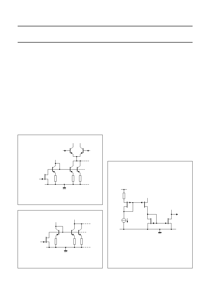
BLOCK DIAGRAM
handbook, full pagewidth
LASER
CONTROL
BLOCK
BAND GAP
REFERENCE
data input
(differential)
TZA3041AHL
CURRENT
SWITCH
ALARMHI
TZERO
2
DIN
MONIN
28
18
ALARMLO
21
5
TONE
4
ALARM
26
22
ONE
23
ZERO
13
LA
DINQ
29
12
LAQ
15
BIAS
6
BGAP
MBK874
ALS
31
VCC(B)
10
GND
1, 3, 8, 9,
11, 14, 16, 17
24, 25, 32
VCC(G)
7
VCC(R)
19, 20
27, 30
4
11
Fig.1 Block diagram of TZA3041AHL.
handbook, full pagewidth
MBK873
LASER
CONTROL
BLOCK
BAND GAP
REFERENCE
TZA3041BHL
CURRENT
SWITCH
MUX
TZERO
ALS
2
DLOOP
MONIN
19
31
VCC(B)
10
GND
1, 3, 8, 9,
11, 14, 16, 17
24, 25, 32
VCC(G)
7
ENL
26
5
TONE
4
22
ONE
23
ZERO
13
LA
DLOOPQ
20
DIN
28
DINQ
29
12
LAQ
15
BIAS
6
BGAP
VCC(R)
18, 21
27, 30
4
11
Fig.2 Block diagram of TZA3041BHL.

2002 Aug 13
4
Philips Semiconductors
Product specification
Gigabit Ethernet/Fibre Channel laser
drivers
TZA3041AHL; TZA3041BHL;
TZA3041U
PINNING
SYMBOL
PIN
PAD
DESCRIPTION
TZA3041AHL TZA3041BHL
TZA3041U
GND
1
1
1
ground
MONIN
2
2
2
monitor photodiode current input
GND
3
3
3
ground
IGM
-
-
4
not connected
TONE
4
4
5
connection for external capacitor used for setting
optical 1 control loop time constant (optional)
TZERO
5
5
6
connection for external capacitor used for setting
optical 0 control loop time constant (optional)
BGAP
6
6
7
connection for external band gap decoupling
capacitor
V
CC(G)
7
7
8
supply voltage (green domain); note 1
V
CC(G)
-
-
9
supply voltage (green domain); note 1
GND
8
8
10
ground
GND
9
9
11
ground
V
CC(B)
10
10
12
supply voltage (blue domain); note 2
V
CC(B)
-
-
13
supply voltage (blue domain); note 2
GND
11
11
14
ground
LAQ
12
12
15
laser modulation output inverted
LA
13
13
16
laser modulation output
GND
14
14
17
ground
BIAS
15
15
18
laser bias current output
GND
16
16
19
ground
GND
17
17
20
ground
GND
-
-
21
ground
ALARMHI
18
-
22
maximum bias current alarm reference level input
V
CC(R)
-
18
23
supply voltage (red domain); note 3
V
CC(R)
19
-
-
supply voltage (red domain); note 3
DLOOP
-
19
24
loop mode data input
V
CC(R)
20
-
-
supply voltage (red domain); note 3
DLOOPQ
-
20
25
loop mode data input inverted
V
CC(R)
-
-
26
supply voltage (red domain); note 3
ALARMLO
21
-
27
minimum bias current alarm reference level input
V
CC(R)
-
21
-
supply voltage (red domain); note 3
ONE
22
22
28
optical 1 reference level input
ZERO
23
23
29
optical 0 reference level input
GND
24
24
30
ground
GND
25
25
31
ground
ALARM
26
-
32
alarm output
ENL
-
26
33
loop mode enable input

2002 Aug 13
5
Philips Semiconductors
Product specification
Gigabit Ethernet/Fibre Channel laser
drivers
TZA3041AHL; TZA3041BHL;
TZA3041U
Notes
1. Supply voltage for the Monitor PhotoDiode (MPD) input current.
2. Supply voltage for the laser modulation outputs (LA, LAQ).
3. Supply voltage for the data inputs (DIN, DINQ), optical 1 and 0 reference level inputs (ONE, ZERO), and the bias
current alarm reference level inputs (ALARMHI, ALARMLO).
V
CC(R)
27
27
34
supply voltage (red domain); note 3
DIN
28
28
35
data input
DINQ
29
29
36
data input inverted
V
CC(R)
30
30
37
supply voltage (red domain); note 3
ALS
31
31
38
automatic laser shutdown input
GND
32
32
39
ground
GND
-
-
40
ground
SYMBOL
PIN
PAD
DESCRIPTION
TZA3041AHL TZA3041BHL
TZA3041U
handbook, full pagewidth
TZA3041AHL
MBK870
1
2
3
4
5
6
7
8
24
23
22
21
20
19
18
17
9
10
11
12
13
14
15
16
32
31
30
29
28
27
26
25
GND
MONIN
GND
TONE
TZERO
BGAP
VCC(G)
GND
GND
V
CC(B)
GND
LAQ
GND
BIAS
GND
LA
GND
ALARMHI
VCC(R)
ONE
ALARMLO
ZERO
VCC(R)
GND
GND
DIN
DINQ
V
CC(R)
ALS
GND
ALARM
V
CC(R)
Fig.3 Pin configuration of TZA3041AHL.

2002 Aug 13
6
Philips Semiconductors
Product specification
Gigabit Ethernet/Fibre Channel laser
drivers
TZA3041AHL; TZA3041BHL;
TZA3041U
handbook, full pagewidth
TZA3041BHL
MBK875
1
2
3
4
5
6
7
8
24
23
22
21
20
19
18
17
9
10
11
12
13
14
15
16
32
31
30
29
28
27
26
25
GND
MONIN
GND
TONE
TZERO
BGAP
VCC(G)
GND
GND
V
CC(B)
GND
LAQ
GND
BIAS
GND
LA
GND
VCC(R)
DLOOPQ
ONE
VCC(R)
ZERO
DLOOP
GND
GND
DIN
DINQ
V
CC(R)
ALS
GND
ENL
V
CC(R)
Fig.4 Pin configuration of TZA3041BHL.
FUNCTIONAL DESCRIPTION
The TZA3041AHL, TZA3041BHL and TZA3041U laser
drivers accept a 1.2 Gbits/s Non-Return to Zero (NRZ)
input data stream, and generate an output signal with
sufficient current to drive a solid state Fabry Perot (FP) or
Distributed FeedBack (DFB) laser. They also contain dual
loop control circuitry for stabilizing the true laser optical
power levels representing logic 1 and logic 0.
The input buffers present a high impedance to the data
stream on the differential inputs (pins DIN and DINQ);
see Fig.5. The input signal can be at a CML level of
approximately 200 mV (p-p) below the supply voltage, or
at a PECL level up to 800 mV (p-p). The inputs can be
configured to accept CML signals by connecting pins DIN
and DINQ to V
CC(R)
via external 50
pull-up resistors.
If PECL compatibility is required, the usual Thevenin
termination can be applied.
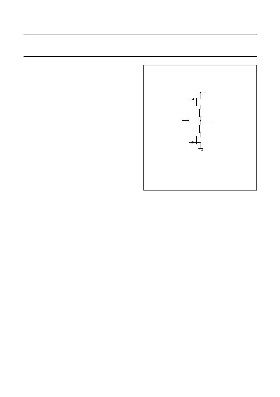
handbook, full pagewidth
MGS910
10 k
10 k
DINQ, DLOOPQ
DIN, DLOOP
100
GND
VCC(R)
100
Fig.5 DIN/DINQ and DLOOP/DLOOPQ inputs.
2002 Aug 13
7
Philips Semiconductors
Product specification
Gigabit Ethernet/Fibre Channel laser
drivers
TZA3041AHL; TZA3041BHL;
TZA3041U
For ECL signals (negative and referenced to ground), the
inputs should be AC-coupled to the signal source.
If AC-coupling is applied, a constant input signal (either
LOW or HIGH) will cause the device to be in an undefined
state. To avoid this, it is recommended to apply a slight
offset to the input stage. The applied offset must be higher
than the specified value in Chapter "Characteristics", but
much lower than the applied input voltage swing.
The RF path is fully differential and contains a differential
preamplifier and a main amplifier. The main amplifier is
able to operate at the large peak currents required at the
output laser driver stage and is insensitive to supply
voltage variations. The output signal from the main
amplifier drives a current switch which supplies a
guaranteed maximum modulation current of 60 mA to
pins LA and LAQ (see Fig.6). The BIAS pin outputs a
guaranteed maximum DC bias current of up to 90 mA for
adjusting the optical laser output to a level above its light
emitting threshold (see Fig.7).
Automatic laser control
A laser with a Monitor PhotoDiode (MPD) is required for
the laser control circuit (see application diagrams
Figs 18 and 19).
The MPD current is proportional to the laser emission and
is applied to pin MONIN. The MPD current range is
100 to 1000
µ
A (p-p). The input buffer is optimized to cope
with an MPD capacitance of up to 50 pF. To prevent the
input buffer from oscillating if the MPD capacitance is low,
the capacitance should be increased to the minimum value
specified in Chapter "Characteristics", by connecting a
capacitor between pin MONIN and V
CC(G)
.
DC reference currents are applied to pins ONE and ZERO
to set the MPD reference levels for laser HIGH and laser
LOW respectively. This is adequately achieved by using
resistors to connect V
CC(R)
to pins ONE and ZERO
(see Fig.8), however, current DACs can also be used. The
voltages on pins ONE and ZERO are held at a constant
level of 1.5 V below V
CC(R)
. The reference current applied
to pin ONE is internally multiplied by 16 and the reference
current flowing into pin ZERO is internally multiplied by 4.
The accuracy of the V
CC(R)
-
1.5 V voltage at pins ONE
and ZERO is described in Section "Accuracy of voltage on
inputs: ONE, ZERO, ALARMLO, ALARMHI".
handbook, halfpage
MGS906
GND
LA
LAQ
ALS
TR
TRn
Fig.6 LA and LAQ outputs.
handbook, halfpage
MGS907
GND
BIAS
ALS
TR
TRn
Fig.7 Laser driver bias current output circuit.
handbook, halfpage
MGS908
VCC(R)
GND
ONE, ZERO, ALARMLO, ALARMHI
50
µ
A
30 k
Fig.8
ONE, ZERO, ALARMLO and ALARMHI
inputs.

2002 Aug 13
8
Philips Semiconductors
Product specification
Gigabit Ethernet/Fibre Channel laser
drivers
TZA3041AHL; TZA3041BHL;
TZA3041U
The reference current and the resistor for the optical 1
modulation current control loop is calculated using the
following formulae:
(1)
(2)
The reference current and resistor for the optical 0 bias
current control loop is calculated using the following
formulae:
(3)
(4)
In these formulae, I
MPD(ONE)
and I
MPD(ZERO)
represent the
MPD current during an optical 1 and an optical 0 period,
respectively.
E
XAMPLE
A laser operates at optical output power levels of 0.3 mW
for laser HIGH and 0.03 mW for laser LOW (extinction ratio
of 10 dB). Suppose the corresponding MPD currents for
this particular laser are 260 and 30
µ
A, respectively.
In this example, the reference current flowing into
pin ONE is:
This current can be set using a current source or simply by
a resistor of the appropriate value connected between
pin ONE and V
CC(R)
.
In this example, the resistor is:
In this example, the reference current at pin ZERO is:
and can be set using a resistor:
It should be noted that the MPD current is stabilized rather
than the actual laser optical output power. Any deviations
between optical output power and MPD current, known as
`tracking errors', cannot be corrected.
Designing the modulation and bias current control
loop
The optical 1 and 0 current control loop time constants are
determined by on-chip capacitances. If the resulting time
constants are found to be too small in a specific
application, they can be increased by connecting a
capacitor between pins TZERO and TONE.
The optical 1 modulation current control loop time
constant (
) and bandwidth (B) can be estimated using the
following formulae:
(5)
(6)
The optical 0 bias current control loop time constant and
bandwidth can be estimated using the following formulae:
(7)
(8)
The term
LASER
(dimensionless) in the above formulae is
the product of the following two terms:
∑
EO
is the electro-optical efficiency which accounts for
the steepness of the laser slope characteristic. It defines
the rate at which the optical output power increases with
modulation current, and is measured in W/A.
∑
R is the MPD responsivity. It determines the amount of
MPD current for a given value of optical output power,
and is measured in A/W.
E
XAMPLE
A laser with an MPD has the following specifications:
P
O
= 1 mW, I
th
= 25 mA,
EO
= 30 mW/A, R = 500 mA/W.
The term I
th
is the required threshold current to switch on
the laser. If the laser operates just above the threshold
level, it may be assumed that
EO
near the optical 0 level
is 50% of
EO
near the optical 1 level, due to the slope
decreasing near the threshold level.
I
ref ONE
(
)
1
16
------
I
MPD(ONE)
◊
=
A
[ ]
R
ONE
1.5
I
ONE
-----------
24
I
MPD(ONE)
------------------------
=
=
[ ]
I
ref ZERO
(
)
1
4
---
I
MPD(ZERO)
◊
=
A
[ ]
R
ZERO
1.5
I
ZERO
--------------
6
I
MPD(ZERO)
---------------------------
=
=
[ ]
I
ref ONE
(
)
1
16
------
260
10
◊
6
≠
◊
16.25
µ
A
=
=
R
ONE
1.5
16.25
10
6
≠
◊
---------------------------------
92.3 k
=
=
I
ref ZERO
(
)
1
4
---
30
10
6
≠
◊
◊
7.5
µ
A
=
=
R
ZERO
1.5
7.5
10
6
≠
◊
--------------------------
200 k
=
=
ONE
40
10
12
≠
C
TONE
+
◊
(
)
80
10
3
◊
LASER
----------------------
◊
=
s
[ ]
B
ONE
1
2
ONE
◊
--------------------------
=
Hz
[
]
B
ONE
LASER
2
40
10
12
≠
◊
C
TONE
+
(
)
◊
80
◊
10
3
◊
-------------------------------------------------------------------------------------------------
Hz
[
]
=
ZERO
40
10
12
≠
C
TZERO
+
◊
(
)
50
10
3
◊
LASER
----------------------
◊
=
s
[ ]
B
ZERO
1
2
ZERO
◊
----------------------------
=
Hz
[
]
B
ZERO
LASER
2
40
10
12
≠
C
TZERO
+
◊
(
)
◊
50
◊
10
3
◊
----------------------------------------------------------------------------------------------------
Hz
[
]
=

2002 Aug 13
9
Philips Semiconductors
Product specification
Gigabit Ethernet/Fibre Channel laser
drivers
TZA3041AHL; TZA3041BHL;
TZA3041U
In this example, the resulting bandwidth for the optical 1
modulation current control loop, without an external
capacitor, is:
The resulting bandwidth for the optical 0 bias current
control loop, without an external capacitor, is:
It is not necessary to add additional capacitance with this
type of laser.
Control loop data pattern and bit rate dependency
The constants in equations (1) and (3) are valid when the
data pattern frequently contains a sufficient number of
`constant zeroes' and `constant ones'. A single control loop
time period (
ONE
and
ZERO
) must contain ones and zeros
for at least approximately 6 ns. When using the IC in
1.2 Gbits/s applications, the optical extinction ratio will be
slightly higher when compared with slower line rates.
Therefore, it is important to use the actual data patterns
and bit rate of the final application circuit for adjusting the
optical levels.
The laser driver peak detectors are able to track MPD
output current overshoot and undershoot conditions.
Unfortunately, these conditions affect the ability of the IC
to correctly interpret the high and low level MPD current.
In particular, the occurrence of undershoot can have a
markedly adverse effect on the interpretation of the low
level MPD current.
Additional bias by modulation `off' current
Although during operation, the full modulation current
switches between outputs LA and LAQ, a small amount of
modulation current continues to flow through the inactive
pin.
For example, when the laser, whose cathode is connected
to LA, is in the `dark' part of its operating cycle (logic 0),
some of the modulation `off' current flows through LA while
most of the current flows through LAQ. This value
I
o(mod)(off)
is effectively added to the bias current and is
subtracted from the modulation current. Fortunately, the
value correlates closely with the magnitude of the
modulation current. Therefore, applications requiring low
bias and low modulation are less affected. Figure 9 shows
the modulation `off' current as a function of the modulation
`on' current.
Monitoring the bias and modulation current
Although not recommended, the bias and modulation
currents generated by the laser driver can be monitored by
measuring the voltages on pins TZERO and TONE,
respectively (see Fig.10). The relationship between these
voltages and the corresponding currents are given as
transconductance values and are specified in
Chapter "Characteristics". The voltages on pins TZERO
and TONE range from 1.4 to 3.4 V. Any connection to
these pins should have a very high impedance value. It is
mandatory to use a CMOS buffer or an amplifier with an
input impedance higher than 100 G
and with an
extremely low input leakage current (pA).
B
ONE
30
10
3
≠
◊
500
◊
10
3
≠
◊
2
40
◊
10
12
≠
◊
80
◊
10
3
◊
---------------------------------------------------------------------
750 Hz
=
B
ZERO
0.5
30
◊
10
3
≠
◊
500
◊
10
3
≠
◊
2
40
◊
10
12
≠
◊
50
◊
10
3
◊
-------------------------------------------------------------------------
600 Hz
=
handbook, halfpage
0
20
40
60
3
1
0
2
MGS902
Io(mod)(on) (mA)
(2)
(1)
Io(mod)(off)
(mA)
Fig.9 I
o(mod)(off)
as a function of I
o(mod)(on)
.
(1) Worst case operation (T
j
= 125
∞
C, V
CC
= 5.5 V
and worst case parameter processes).
(2) Typical operation.

2002 Aug 13
10
Philips Semiconductors
Product specification
Gigabit Ethernet/Fibre Channel laser
drivers
TZA3041AHL; TZA3041BHL;
TZA3041U
Automatic laser shut-down and laser slow start
The laser modulation and bias currents can be rapidly
switched off when a HIGH level (CMOS) is applied to
pin ALS. This function allows the circuit to be shut-down in
the event of an optical system malfunction. A 25 k
pull-down resistor defaults pin ALS to the non active state
(see Fig.11).
When a LOW level is applied to pin ALS, the modulation
and bias currents slowly increase to the desired values at
the typical time constants of
ONE
and
ZERO
, respectively.
This can be used to slow-start the laser.
Manual laser override
The automatic laser control function can be overridden by
connecting voltage sources to pins TZERO and TONE to
take direct control of the current sources for bias and
modulation respectively. The control voltages should
range from 1.4 to 3.4 V to swing the modulation current
over the range 1 to 60 mA and the bias current over the
range 1 to 90 mA. These current ranges are guaranteed.
Due to the tolerance range in the manufacturing process,
some devices may have higher current values than those
specified, as shown in Figs 12 and 13. Both figures show
that temperature changes cause a slight tilting of the linear
characteristic around an input voltage of 2.4 V.
Consequently, the manually controlled current level is
most insensitive to temperature variations at around this
value. Bias and modulation currents in excess of the
specified range are not supported and should be avoided.
Currents into or out of pins TZERO and TONE in excess of
10
µ
A must be avoided to prevent damage to the circuit.
handbook, halfpage
MGS905
GND
40 pF
<
1 nA
LINEAR VOLTAGE TO
CURRENT CONVERTER
TZERO, TONE
2.4 V
<
1 nA
Fig.10 TZERO and TONE internal configuration.
handbook, halfpage
MGS911
25 k
VCC(R)
100
GND
ALS
100
Fig.11 ALS input.

2002 Aug 13
11
Philips Semiconductors
Product specification
Gigabit Ethernet/Fibre Channel laser
drivers
TZA3041AHL; TZA3041BHL;
TZA3041U
handbook, full pagewidth
3.9
160
120
40
0
1.4
1.9
3.4
80
2.9
2.4
MGS904
Io(mod)
(mA)
VTONE (V)
(3)
(4)
(1)
(5)
specified range
(2)
Fig.12 Modulation current with variation in T
j
and tolerance range in the manufacturing process.
(1) T
j
= 25
∞
C (device with characteristics at upper limit of manufacturing tolerance range).
(2) T
j
= 25
∞
C (typical device).
(3) T
j
=
-
40
∞
C (typical device).
(4) T
j
= 125
∞
C (typical device).
(5) T
j
= 25
∞
C (device with characteristics at lower limit of manufacturing tolerance range).

2002 Aug 13
12
Philips Semiconductors
Product specification
Gigabit Ethernet/Fibre Channel laser
drivers
TZA3041AHL; TZA3041BHL;
TZA3041U
handbook, full pagewidth
3.9
160
120
40
0
1.4
1.9
3.4
80
2.9
2.4
MGS903
IO(BIAS)
(mA)
VTZERO (V)
(2)
(3)
(4)
(5)
(1)
specified range
Fig.13 Bias current with variation in T
j
and tolerance range in the manufacturing process.
(1) T
j
= 25
∞
C (device with characteristics at upper limit of manufacturing tolerance range).
(2) T
j
= 25
∞
C (typical device).
(3) T
j
=
-
40
∞
C (typical device).
(4) T
j
= 125
∞
C (typical device).
(5) T
j
= 25
∞
C (device with characteristics at lower limit of manufacturing tolerance range).
2002 Aug 13
13
Philips Semiconductors
Product specification
Gigabit Ethernet/Fibre Channel laser
drivers
TZA3041AHL; TZA3041BHL;
TZA3041U
Bias alarm for TZA3041AHL
The bias current alarm circuit detects whenever the bias
current is outside a predefined range, and generates a
flag. This feature can detect excessive bias current due to
laser ageing or laser malfunctioning. The current applied
to pin ALARMHI should be the maximum permitted bias
current value attenuated by a ratio of 1:1500. The current
applied to pin ALARMLO should be the minimum
permitted bias current value attenuated by a ratio of 1:300.
Like the reference currents for the laser current control
loop, the alarm reference currents can be set by
connecting external resistors between V
CC(R)
and
pins ALARMHI and ALARMLO (see Fig.8). The resistor
values can be calculated using the following formulae:
(9)
(10)
Example: The following reference currents are required to
limit the bias current range from 6 to 90 mA:
and
The corresponding resistor values are:
and
If the alarm condition is true, the voltage on pin ALARM
(see Fig.14) goes to a HIGH level (CMOS). This signal
could be used, for example, to drive pin ALS to disable the
laser driver; the signal to pin ALS has to be latched to
prevent oscillation.
A hysteresis of approximately 10% is applied to both alarm
functions. The attenuation ratios of 1:300 and 1:1500 are
valid if the bias current rises above the reference current
levels. If the bias current decreases, the ratios are 10%
lower.
Accuracy of voltage on inputs: ONE, ZERO,
ALARMLO, ALARMHI
It is important to consider the accuracy of the 1.5 V level
with respect to V
CC(R)
on pins ONE and ZERO if resistors
are used to set the reference currents. Although this value
is independent of V
CC(R)
, deviations from 1.5 V can be
caused by:
∑
Input current: At T
j
= 25
∞
C, the voltage between pin and
V
CC
varies from 1.58 V at an input current of 6
µ
A, down
to 1.45 V at 65
µ
A and 1.41 V at 100
µ
A. The range
between 65
µ
A and 100
µ
A is only specified for
ALARMLO. In the application, the input current is
virtually fixed, so this variation has little effect.
∑
Variation in batch and individual device characteristics,
not exceeding
±
2% from the nominal product: This
variation can be compensated for where devices in the
application are individually trimmed.
∑
Temperature: The variation in T
j
is shown in Fig.15.
At 30
µ
A (middle of the specified range) the total
variation in T
j
is <1%, at 65
µ
A it is <2% and at 6
µ
A it is
<3%.
R
ALARMHI
1.5
1500
◊
I
O BIAS
(
)
max
(
)
---------------------------------
=
[ ]
R
ALARMLO
1.5
300
◊
I
O BIAS
(
)
min
(
)
--------------------------------
=
[ ]
I
ALARMLO
6
10
3
≠
◊
300
---------------------
20
µ
A
=
=
I
ALARMHI
90
10
3
≠
◊
1500
------------------------
60
µ
A
=
=
R
ALARMHI
1.5
1500
◊
90
10
3
≠
◊
----------------------------
25 k
=
=
R
ALARMLO
1.5
300
◊
6
10
3
≠
◊
------------------------
75 k
=
=
handbook, halfpage
MGS909
20
43
VCC(R)
GND
ALARM
Fig.14 ALARM output.

2002 Aug 13
14
Philips Semiconductors
Product specification
Gigabit Ethernet/Fibre Channel laser
drivers
TZA3041AHL; TZA3041BHL;
TZA3041U
handbook, full pagewidth
150
-
1.65
-
1.55
-
1.45
-
1.60
-
1.50
-
1.40
-
1.35
-
50
-
40
125
0
100
50
MGS901
Vref
(1)
(V)
Tj (
∞
C)
(2)
(3)
(4)
(3)
(4)
(2)
(3)
(4)
Iref =
6
µ
A
Iref =
30
µ
A
Iref =
65
µ
A
(2)
Fig.15 V
ref
on pins ONE, ZERO, ALARMLO and ALARMHI with variation in T
j
and I
ref
.
(1) Referenced to V
CC(R)
.
(2) Upper limit of manufacturing tolerance range.
(3) Nominal product.
(4) Lower limit of manufacturing tolerance range.

2002 Aug 13
15
Philips Semiconductors
Product specification
Gigabit Ethernet/Fibre Channel laser
drivers
TZA3041AHL; TZA3041BHL;
TZA3041U
Loop mode for TZA3041BHL
The loop mode allows the total system application to be
tested. It allows for uninhibited optical transmission
through the fibre front-end (from the MPD through the
transimpedance stage and the data and clock recovery
unit, to the laser driver and via the laser back to the fibre).
Note that the optical receiver used in conjunction with the
TZA3041BHL must have a loop mode output in order to
complete the test loop.
The loop mode is selected by a HIGH level on pin ENL.
By default, pin ENL is pulled to a LOW level by a 25 k
pull-down resistor (see Fig.16).
Power supply connections
Refer to application diagrams Figs 18 and 19. Three
separate supply domains (labelled V
CC(G)
, V
CC(B)
, and
V
CC(R)
) provide isolation between the MPD current input,
the high-current outputs, and the PECL or CML inputs.
Each supply domain should be connected to a central V
CC
via separate filters as shown in Figs 18 and 19. All supply
pins must be connected. The voltage supply levels
should be equal to, and in accordance with, the values
specified in Chapter "Characteristics".
To maximize power supply isolation, the cathode of the
MPD should be connected to V
CC(G)
and the anode of the
laser diode should be connected to V
CC(B)
. It is
recommended that the laser diode anode is also
connected to a separate decoupling capacitor C9.
Generally, the inverted laser modulation output (pin LAQ)
is not used. To correctly balance the output stage, an
equalization network (Z1) with an impedance comparable
to the laser diode is connected between pin LAQ and
V
CC(B)
.
All external components should be surface mounted
devices, preferably of size 0603 or smaller.
The components must be mounted as close to the IC as
possible.
It is especially recommended to mount the following
components very close to the IC:
∑
Power supply decoupling capacitors C2, C3 and C4
∑
Input matching network on pins DIN, DINQ, DLOOP and
DLOOPQ
∑
Capacitor C5 on pin MONIN
∑
Output matching network Z1 at the unused output
∑
The laser.
Bare die ground
In addition to the separate V
CC
domains, the bare die
contains three corresponding ground (GND) domains.
Isolation between the GND domains is limited due to the
finite substrate conductance.
Mount the die preferably on a large and highly conductive
grounded die pad. All GND pads must be bonded to the
die pad. The external ground is thus ideally combined with
the die ground to avoid ground bounce problems.
Layout recommendations
Layout recommendations for the TZA3041AHL and
TZA3041BHL can be found in application note
"AN98090
Fiber optic transceiverboard STM1/4/8, OC3,12,24,
FC/GE".
handbook, halfpage
MGS912
25 k
VCC(R)
GND
ENL
600
Fig.16 ENL input.

2002 Aug 13
16
Philips Semiconductors
Product specification
Gigabit Ethernet/Fibre Channel laser
drivers
TZA3041AHL; TZA3041BHL;
TZA3041U
LIMITING VALUES
In accordance with the Absolute Maximum Rating System (IEC 60134).
THERMAL CHARACTERISTICS
SYMBOL
PARAMETER
MIN.
MAX.
UNIT
V
CC
supply voltage
-
0.5
+6
V
V
n
DC voltage on
pin MONIN
1.3
V
CC
+ 0.5
V
pins TONE and TZERO
-
0.5
V
CC
+ 0.5
V
pin BGAP
-
0.5
+3.2
V
pin BIAS
-
0.5
V
CC
+ 0.5
V
pins LA and LAQ
1.3
V
CC
+ 0.5
V
pin ALS
-
0.5
V
CC
+ 0.5
V
pins ONE and ZERO
-
0.5
V
CC
+ 0.5
V
pins DIN and DINQ
-
0.5
V
CC
+ 0.5
V
pin ALARM (TZA3041AHL)
-
0.5
V
CC
+ 0.5
V
pins ALARMHI and ALARMLO (TZA3041AHL)
-
0.5
V
CC
+ 0.5
V
pins DLOOP and DLOOPQ (TZA3041BHL)
-
0.5
V
CC
+ 0.5
V
pin ENL (TZA3041BHL)
-
0.5
V
CC
+ 0.5
V
I
n
DC current on
pin MONIN
-
0.5
+2.5
mA
pins TONE and TZERO
-
0.5
+0.5
mA
pin BGAP
-
2.0
+2.5
mA
pin BIAS
-
0.5
+200
mA
pins LA and LAQ
-
0.5
+100
mA
pin ALS
-
0.5
+0.5
mA
pins ONE and ZERO
-
0.5
+0.5
mA
pins DIN and DINQ
-
0.5
+0.5
mA
pin ALARM (TZA3041AHL)
-
0.5
+10
mA
pins ALARMHI and ALARMLO (TZA3041AHL)
-
0.5
+0.5
mA
pins DLOOP and DLOOPQ (TZA3041BHL)
-
0.5
+0.5
mA
pin ENL (TZA3041BHL)
-
0.5
+0.5
mA
T
amb
ambient temperature
-
40
+85
∞
C
T
j
junction temperature
-
40
+125
∞
C
T
stg
storage temperature
-
65
+150
∞
C
SYMBOL
PARAMETER
VALUE
UNIT
R
th(j-s)
thermal resistance from junction to solder point
15
K/W
R
th(j-c)
thermal resistance from junction to case
23
K/W

2002 Aug 13
17
Philips Semiconductors
Product specification
Gigabit Ethernet/Fibre Channel laser
drivers
TZA3041AHL; TZA3041BHL;
TZA3041U
CHARACTERISTICS
V
CC
= 4.5 to 5.5 V; T
amb
=
-
40 to +85
∞
C; all voltages measured with respect to GND.
SYMBOL
PARAMETER
CONDITIONS
MIN.
TYP.
MAX.
UNIT
Supplies
V
CC
supply voltage
4.5
5.0
5.5
V
I
CC(R)
supply current (R)
-
4
10
mA
I
CC(G)
supply current (G)
12
18
26
mA
I
CC(B)
supply current (B)
ALS LOW; note 1
20
41
65
mA
ALS HIGH
-
3
5
mA
I
CC(tot)
total supply current
ALS LOW; note 1
32
63
101
mA
ALS HIGH
12
25
41
mA
P
tot
total power dissipation
ALS LOW; note 2
145
430
925
mW
ALS HIGH; note 2
50
125
225
mW
Data inputs: pins DIN and DINQ (and pins DLOOP and DLOOPQ on TZA3041BHL); see Fig.17
V
i(p-p)
input voltage
(peak-to-peak value)
single-ended
100
250
800
mV
V
IO
input offset voltage
-
25
-
+25
mV
V
I(min)
minimum input voltage
V
CC(R)
-
2
-
-
V
V
I(max)
maximum input voltage
-
-
V
CC(R)
+ 0.25 V
Z
i
input impedance
for low frequencies;
single-ended
7
10
13
k
CMOS inputs: pin ALS (and pin ENL on TZA3041BHL)
V
IL
LOW-level input voltage
-
-
2
V
V
IH
HIGH-level input voltage
3
-
-
V
R
pd(ALS)
internal pull-down
resistance on pin ALS
21
25.5
30
k
R
pd(ENL)
internal pull-down
resistance on pin ENL
15
25
35
k
CMOS output: pin ALARM (on TZA3041AHL)
V
OL
LOW-level output voltage
I
OH
=
-
200
µ
A
0
-
0.2
V
V
OH
HIGH-level output voltage
I
OH
= 200
µ
A
V
CC
-
0.2
-
V
CC
V
Monitor photodiode input: pin MONIN
V
I
DC input voltage
1.2
1.8
2.4
V
I
MPD
monitor photodiode
current
laser optical 0
24
-
260
µ
A
laser optical 1
96
-
1040
µ
A
C
MPD
monitor photodiode
capacitance
note 3
30
-
50
pF

2002 Aug 13
18
Philips Semiconductors
Product specification
Gigabit Ethernet/Fibre Channel laser
drivers
TZA3041AHL; TZA3041BHL;
TZA3041U
Control loop reference current inputs: pins ONE and ZERO
I
ref(ONE)
reference current on
pin ONE
note 4
6
-
65
µ
A
V
ref(ONE)
reference voltage on
pin ONE
referenced to V
CC(R)
;
note 5
-
-
1.5
-
V
(ONE)
attenuation ratio of I
ref(ONE)
to I
MPD(ONE)
note 6
-
16
-
-
I
ref(ZERO)
reference current on
pin ZERO
note 4
6
-
65
µ
A
V
ref(ZERO)
reference voltage on
pin ZERO
referenced to V
CC(R)
;
note 5
-
-
1.5
-
V
(ZERO)
attenuation ratio of
I
ref(ZERO)
to I
MPD(ZERO)
note 6
-
4
-
-
Control loop time constants: pins TONE and TZERO
V
TONE
voltage on pin TONE
floating output
1.4
-
3.4
V
g
m(TONE)
transconductance of
pin TONE
note 7
60
95
130
mA/V
V
TZERO
voltage on pin TZERO
floating output
1.4
-
3.4
V
g
m(TZERO)
transconductance of
pin TZERO
note 8
100
145
190
mA/V
Laser modulation current outputs: pins LA and LAQ
I
o(mod)(on)
modulation output current
(active pin)
note 9
2.5
-
60
mA
I
o(mod)(off)
modulation output current
(inactive pin)
I
o(mod)(on)
= 30mA
-
-
0.5
mA
I
o(mod)(on)
= 60mA
-
-
2.8
mA
I
o(mod)(ALS)
output current during laser
shutdown
-
-
10
µ
A
V
O
output voltage
2
-
5
V
t
r
current rise time
note 10
-
120
200
ps
t
f
current fall time
note 10
-
120
200
ps
J
o(p-p)
intrinsic electrical output
jitter (peak-to-peak value)
note 11
-
-
50
mUI
Laser bias current output: pin BIAS
I
O(BIAS)
bias output current
note 12
2.8
-
90
mA
I
O(BIAS)(ALS)
output current during laser
shutdown
-
-
10
µ
A
t
res(off)
response time after laser
shutdown
I
O(BIAS)
= 90 mA; note 13
-
-
1
µ
s
V
O(BIAS)
bias output voltage
1
-
5
V
SYMBOL
PARAMETER
CONDITIONS
MIN.
TYP.
MAX.
UNIT

2002 Aug 13
19
Philips Semiconductors
Product specification
Gigabit Ethernet/Fibre Channel laser
drivers
TZA3041AHL; TZA3041BHL;
TZA3041U
Notes
1. Supply current:
a) The values do not include the modulation and bias currents through pins LA, LAQ and BIAS.
b) Minimum value refers to V
TONE
= 1.4 V at I
o(mod)(min)
and V
TZERO
= 1.4 V at I
O(BIAS)(min)
.
c) Maximum value refers to V
TONE
= 3.4 V at I
o(mod)(max)
and V
TZERO
= 3.4 V at I
O(BIAS)(max)
.
d) A first order estimate of the typical value of I
CC(tot)
as a function of T
j
, I
o(mod)
, and I
O(BIAS)
is:
I
CC(tot)
=
2. Power dissipation:
a) The value for P
tot
includes the modulation and bias currents through pins LA, LAQ and BIAS.
b) The minimum value for P
tot
is the on-chip dissipation when V
TONE
= 1.4 V at I
o(mod)(min)
, V
LA
= V
LAQ
= 2 V,
V
TZERO
= 1.4 V at I
O(BIAS)(min)
, V
O(BIAS)
= 1 V, and parameter processes are at a minimum.
c) The maximum value for P
tot
is the on-chip dissipation when V
TONE
= 3.4 V at I
o(mod)(max)
, V
LA
= V
LAQ
= 2 V,
V
TZERO
= 3.4 V at I
O(BIAS)(max)
, V
O(BIAS)
= 1 V, and parameter processes are at a maximum.
d) P
tot
= I
CC(tot)
◊
V
CC
+ I
O(BIAS)
◊
V
O(BIAS)
+ I
LA
◊
V
LA
with I
o(mod)(on)
flowing through pin LA.
3. The minimum value of the capacitance on pin MONIN is required to prevent instability.
4. The reference currents can be set by connecting external resistors between V
CC
and pins ONE and ZERO
(see Section "Automatic laser control"). The corresponding MPD current range for optical 1 is from 96 to 1040
µ
A.
The MPD current range for optical 0 is from 24 to 260
µ
A.
5. See Section "Accuracy of voltage on inputs: ONE, ZERO, ALARMLO, ALARMHI".
6. See Section "Automatic laser control".
7. The specified transconductance is the ratio between the modulation current on pins LA or LAQ and the voltage on
pin TONE, under small signal conditions.
Alarm reference current inputs: pins ALARMHI and ALARMLO (TZA3041AHL)
I
ref(ALARMLO)
reference current on
pin ALARMLO
note 14
6
-
100
µ
A
V
ref(ALARMLO)
reference voltage on
pin ALARMLO
referenced to V
CC(R)
-
-
1.5
-
V
(ALARMLO)
attenuation ratio of
I
ref(ALARMLO)
to I
O(BIAS)(min)
note 15
200
315
400
I
O(BIAS)(min)(hys)
minimum bias current
detection hysteresis
7.5
10
15
%
I
ref(ALARMHI)
reference current on
pin ALARMHI
note 14
6
-
65
µ
A
V
ref(ALARMHI)
reference voltage on
pin ALARMHI
referenced to V
CC(R)
-
-
1.5
-
V
(ALARMHI)
attenuation ratio of
I
ref(ALARMHI)
to I
O(BIAS)(max)
note 15
1300
1600
1800
I
O(BIAS)(max)(hys)
maximum bias current
detection hysteresis
7.5
10
15
%
Reference voltage output: pin BGAP
V
O
output voltage
1.165
1.20
1.235
µ
A
SYMBOL
PARAMETER
CONDITIONS
MIN.
TYP.
MAX.
UNIT
55.6 mA
0.0015
+
I
O BIAS
(
)
mA
[
]
I
o mod
(
)
on
(
)
mA
[
]
◊
◊
1
0.026
T
j
∞
C
[
]
25
-----------------
◊
≠
◊

2002 Aug 13
20
Philips Semiconductors
Product specification
Gigabit Ethernet/Fibre Channel laser
drivers
TZA3041AHL; TZA3041BHL;
TZA3041U
8. The specified transconductance is the ratio between the bias current on pin BIAS and the voltage on pin TZERO,
under small signal conditions.
9. These are the guaranteed values; the lowest attainable output current will always be lower than 2.5 mA, and the
highest output current will always be higher than 60 mA.
10. The voltage rise and fall times (20% to 80%) can have larger values due to capacitive effects. Specifications are
guaranteed by design and characterization. Each device is tested at full operating speed to guarantee RF
functionality.
11. Measured according to IEEE 802.3z and ANSI X3.230. The electrically generated (current) jitter is assumed to be
less than 50% of the optical output jitter. The specification is guaranteed by design.
12. These are the guaranteed values; the lowest output current will always be less than 2.8 mA and the highest output
current will always be more than 90 mA.
13. The response time is defined as the delay between the onset of the ramp on pin ALS (at 10% of the HIGH level) and
the extinction of the bias current (at 10% of the original value).
14. The reference currents can be set by connecting a resistor between pin ALARMLO and V
CC(R)
and between
pin ALARMHI and V
CC(R)
; for detailed information, see Section "Bias alarm for TZA3041AHL". The corresponding
low-bias threshold range is 1.8 to 19.5 mA. The high-bias threshold range is 9 to 97.5 mA.
15. See Section "Bias alarm for TZA3041AHL".
handbook, full pagewidth
MGK274
VIO
VI(max)
VI(min)
Vi(p-p)
VCC(R)
Fig.17 Logic level symbol definitions for data inputs.

2002 Aug 13
21
Philips Semiconductors
Product specification
Gigabit Ethernet/Fibre Channel laser
drivers
TZA3041AHL; TZA3041BHL;
TZA3041U
APPLICATION INFORMATION
handbook, full pagewidth
MBK877
R5
18
TZA3041AHL
VCC(R)
TONE
MONIN
11
C6
(3)
TZERO
C7
(4)
BGAP
22 nF
C8
2
4
5
6
1, 3, 8, 9, 11,
14, 16, 17,
24, 25, 32
15
13
12
GND
BIAS
LA
LAQ
19, 20,
27, 30
VCC(B)
VCC(G)
ALS
31
7
10
DINQ
29
DIN
28
ALARM
R1
(5)
R2
(5)
R3
(6)
R4
(6)
26
23
22
data inputs
normal mode
(CML/PECL compatible)
21
18
ALARMHI
laser
C9
MPD
ALARMLO
Z1
(7)
C5
(2)
L1
4
ONE
ZERO
C2
22 nF
VCC
C1
1
µ
F
C3
22 nF
C4
22 nF
(1)
(1)
(1)
Fig.18 Application diagram with the TZA3041AHL configured for 1.2 Gbits/s (Gigabit Ethernet/Fibre Channel).
(1) Ferrite bead e.g. Murata BLM31A601S.
(2) C5 is required to meet the minimum capacitance value on pin MONIN (optional, see Section "Automatic laser control").
(3) C6 enhances modulation control loop time constant (optional).
(4) C7 enhances bias control loop time constant (optional).
(5) R1 and R2 are used for setting optical 0 and optical 1 reference currents (see Section "Automatic laser control").
(6) R3 and R4 are used for setting minimum and maximum bias currents (see Section "Bias alarm for TZA3041AHL").
(7) Z1 is required for balancing the output stage (see Section "Power supply connections").

2002 Aug 13
22
Philips Semiconductors
Product specification
Gigabit Ethernet/Fibre Channel laser
drivers
TZA3041AHL; TZA3041BHL;
TZA3041U
handbook, full pagewidth
MBK876
R3
18
TZA3041BHL
VCC(R)
TONE
MONIN
11
C6
(3)
TZERO
C7
(4)
BGAP
22 nF
C8
2
4
5
6
1, 3, 8, 9, 11,
14, 16, 17,
24, 25, 32
15
13
12
GND
BIAS
LA
LAQ
18, 21,
27, 30
VCC(B)
VCC(G)
ALS
31
7
10
DINQ
29
DIN
28
ENL
R1
(5)
R2
(5)
26
23
22
data inputs
normal mode
(CML/PECL compatible)
20
19
laser
C9
MPD
Z1
(6)
C5
(2)
L1
4
ONE
ZERO
C2
22 nF
(1)
VCC
C1
1
µ
F
C3
22 nF
C4
22 nF
loop mode inputs
(CML/PECL
compatible)
DLOOP
DLOOPQ
(1)
(1)
Fig.19 Application diagram with the TZA3041BHL configured for 1.2 Gbits/s (Gigabit Ethernet/Fibre Channel).
(1) Ferrite bead e.g. Murata BLM31A601S.
(2) C5 is required to meet the minimum capacitance value on pin MONIN (optional, see Section "Automatic laser control").
(3) C6 enhances modulation control loop time constant (optional).
(4) C7 enhances bias control loop time constant (optional).
(5) R1 and R2 are used for setting optical 0 and optical 1 reference currents (see Section "Automatic laser control").
(6) Z1 is required for balancing the output stage (see Section "Power supply connections").

2002 Aug 13
23
Philips Semiconductors
Product specification
Gigabit Ethernet/Fibre Channel laser
drivers
TZA3041AHL; TZA3041BHL;
TZA3041U
BONDING PAD LOCATIONS
Note
1. All x and y coordinates represent the position of the
centre of the pad in
µ
m with respect to the centre of the
die (see Fig.20).
SYMBOL
PAD
COORDINATES
(1)
x
y
GND
1
-
664
-
910
MONIN
2
-
524
-
910
GND
3
-
367
-
910
IGM
4
-
227
-
910
TONE
5
-
70
-
910
TZERO
6
+87
-
910
BGAP
7
+244
-
910
V
CC(G)
8
+384
-
910
V
CC(G)
9
+524
-
910
GND
10
+664
-
910
GND
11
+910
-
630
V
CC(B)
12
+910
-
490
V
CC(B)
13
+910
-
350
GND
14
+910
-
210
LAQ
15
+910
-
70
LA
16
+910
+70
GND
17
+910
+210
BIAS
18
+910
+350
GND
19
+910
+490
GND
20
+910
+630
GND
21
+681
+910
ALARMHI
22
+541
+910
V
CC(R)
23
+384
+910
DLOOP
24
+227
+910
DLOOPQ
25
+87
+910
V
CC(R)
26
-
70
+910
ALARMLO
27
-
210
+910
ONE
28
-
367
+910
ZERO
29
-
524
+910
GND
30
-
681
+910
GND
31
-
910
+681
ALARM
32
-
910
+541
ENL
33
-
910
+384
V
CC(R)
34
-
910
+227
DIN
35
-
910
+70
DINQ
36
-
910
-
70
V
CC(R)
37
-
910
-
227
ALS
38
-
910
-
367
GND
39
-
910
-
551
GND
40
-
910
-
664
SYMBOL
PAD
COORDINATES
(1)
x
y

2002 Aug 13
24
Philips Semiconductors
Product specification
Gigabit Ethernet/Fibre Channel laser
drivers
TZA3041AHL; TZA3041BHL;
TZA3041U
handbook, full pagewidth
MBK871
2 mm
(1)
0
0
TZA3041U
2 mm
(1)
TONE
IGM
GND
MONIN
GND
GND
V
CC(G)
V
CC(G)
BGAP
TZERO
ALARMLO
ZERO
GND
ONE
LAQ
VCC(B)
VCC(B)
GND
ALS
GND
GND
LA
GND
BIAS
GND
GND
GND
ENL
ALARM
GND
VCC(R)
DINQ
DIN
VCC(R)
GND
ALARMHI
V
CC(R)
DLOOP
DLOOPQ
V
CC(R)
x
y
1
2
5
6
7
8
9
10
11
12
13
14
15
16
17
18
19
20
21
22
23
24
25
26
27
28
29
30
3
40
39
38
37
36
35
34
33
32
31
4
Fig.20 Bonding pad locations of TZA3041U.
(1) Typical value.
Table 1
Physical characteristics of bare die
PARAMETER
VALUE
Glass passivation
2.1
µ
m PSG (PhosphoSilicate Glass) on top of 0.7
µ
m silicon nitride
Bonding pad dimension
minimum dimension of exposed metallization is 90
◊
90
µ
m (pad size = 100
◊
100
µ
m)
Metallization
1.2
µ
m AlCu (1% Cu)
Thickness
380
µ
m nominal
Size
2.000
◊
2.000 mm (4.000 mm
2
)
Backing
silicon; electrically connected to GND potential through substrate contacts
Attach temperature
<430
∞
C; glue is recommended for attaching die
Attach time
<15 s

2002 Aug 13
25
Philips Semiconductors
Product specification
Gigabit Ethernet/Fibre Channel laser
drivers
TZA3041AHL; TZA3041BHL;
TZA3041U
PACKAGE OUTLINE
0.2
UNIT
A
max.
A
1
A
2
A
3
b
p
c
E
(1)
e
H
E
L
L
p
Z
y
w
v
REFERENCES
OUTLINE
VERSION
EUROPEAN
PROJECTION
ISSUE DATE
IEC
JEDEC
EIAJ
mm
1.60
0.15
0.05
1.5
1.3
0.25
0.27
0.17
0.18
0.12
5.1
4.9
0.5
7.15
6.85
1.0
0.95
0.55
7
0
o
o
0.12
0.1
DIMENSIONS (mm are the original dimensions)
Note
1. Plastic or metal protrusions of 0.25 mm maximum per side are not included.
0.75
0.45
SOT401-1
136E01
MS-026
99-12-27
00-01-19
D
(1)
(1)
(1)
5.1
4.9
H
D
7.15
6.85
E
Z
0.95
0.55
D
b
p
e
E
B
8
D
H
b
p
E
H
v
M
B
D
ZD
A
Z E
e
v
M
A
X
1
32
25
24
17
16
9
A
1
A
L
p
detail X
L
(A )
3
A
2
y
w
M
w
M
0
2.5
5 mm
scale
LQFP32: plastic low profile quad flat package; 32 leads; body 5 x 5 x 1.4 mm
SOT401-1
c
pin 1 index

2002 Aug 13
26
Philips Semiconductors
Product specification
Gigabit Ethernet/Fibre Channel laser
drivers
TZA3041AHL; TZA3041BHL;
TZA3041U
SOLDERING
Introduction to soldering surface mount packages
This text gives a very brief insight to a complex technology.
A more in-depth account of soldering ICs can be found in
our
"Data Handbook IC26; Integrated Circuit Packages"
(document order number 9398 652 90011).
There is no soldering method that is ideal for all surface
mount IC packages. Wave soldering can still be used for
certain surface mount ICs, but it is not suitable for fine pitch
SMDs. In these situations reflow soldering is
recommended.
Reflow soldering
Reflow soldering requires solder paste (a suspension of
fine solder particles, flux and binding agent) to be applied
to the printed-circuit board by screen printing, stencilling or
pressure-syringe dispensing before package placement.
Several methods exist for reflowing; for example,
convection or convection/infrared heating in a conveyor
type oven. Throughput times (preheating, soldering and
cooling) vary between 100 and 200 seconds depending
on heating method.
Typical reflow peak temperatures range from
215 to 250
∞
C. The top-surface temperature of the
packages should preferable be kept below 220
∞
C for
thick/large packages, and below 235
∞
C for small/thin
packages.
Wave soldering
Conventional single wave soldering is not recommended
for surface mount devices (SMDs) or printed-circuit boards
with a high component density, as solder bridging and
non-wetting can present major problems.
To overcome these problems the double-wave soldering
method was specifically developed.
If wave soldering is used the following conditions must be
observed for optimal results:
∑
Use a double-wave soldering method comprising a
turbulent wave with high upward pressure followed by a
smooth laminar wave.
∑
For packages with leads on two sides and a pitch (e):
≠ larger than or equal to 1.27 mm, the footprint
longitudinal axis is preferred to be parallel to the
transport direction of the printed-circuit board;
≠ smaller than 1.27 mm, the footprint longitudinal axis
must be parallel to the transport direction of the
printed-circuit board.
The footprint must incorporate solder thieves at the
downstream end.
∑
For packages with leads on four sides, the footprint must
be placed at a 45
∞
angle to the transport direction of the
printed-circuit board. The footprint must incorporate
solder thieves downstream and at the side corners.
During placement and before soldering, the package must
be fixed with a droplet of adhesive. The adhesive can be
applied by screen printing, pin transfer or syringe
dispensing. The package can be soldered after the
adhesive is cured.
Typical dwell time is 4 seconds at 250
∞
C.
A mildly-activated flux will eliminate the need for removal
of corrosive residues in most applications.
Manual soldering
Fix the component by first soldering two
diagonally-opposite end leads. Use a low voltage (24 V or
less) soldering iron applied to the flat part of the lead.
Contact time must be limited to 10 seconds at up to
300
∞
C.
When using a dedicated tool, all other leads can be
soldered in one operation within 2 to 5 seconds between
270 and 320
∞
C.

2002 Aug 13
27
Philips Semiconductors
Product specification
Gigabit Ethernet/Fibre Channel laser
drivers
TZA3041AHL; TZA3041BHL;
TZA3041U
Suitability of surface mount IC packages for wave and reflow soldering methods
Notes
1. For more detailed information on the BGA packages refer to the
"(LF)BGA Application Note" (AN01026); order a copy
from your Philips Semiconductors sales office.
2. All surface mount (SMD) packages are moisture sensitive. Depending upon the moisture content, the maximum
temperature (with respect to time) and body size of the package, there is a risk that internal or external package
cracks may occur due to vaporization of the moisture in them (the so called popcorn effect). For details, refer to the
Drypack information in the
"Data Handbook IC26; Integrated Circuit Packages; Section: Packing Methods".
3. These packages are not suitable for wave soldering. On versions with the heatsink on the bottom side, the solder
cannot penetrate between the printed-circuit board and the heatsink. On versions with the heatsink on the top side,
the solder might be deposited on the heatsink surface.
4. If wave soldering is considered, then the package must be placed at a 45
∞
angle to the solder wave direction.
The package footprint must incorporate solder thieves downstream and at the side corners.
5. Wave soldering is suitable for LQFP, TQFP and QFP packages with a pitch (e) larger than 0.8 mm; it is definitely not
suitable for packages with a pitch (e) equal to or smaller than 0.65 mm.
6. Wave soldering is suitable for SSOP and TSSOP packages with a pitch (e) equal to or larger than 0.65 mm; it is
definitely not suitable for packages with a pitch (e) equal to or smaller than 0.5 mm.
PACKAGE
(1)
SOLDERING METHOD
WAVE
REFLOW
(2)
BGA, LBGA, LFBGA, SQFP, TFBGA, VFBGA
not suitable
suitable
HBCC, HBGA, HLQFP, HSQFP, HSOP, HTQFP, HTSSOP, HVQFN,
HVSON, SMS
not suitable
(3)
suitable
PLCC
(4)
, SO, SOJ
suitable
suitable
LQFP, QFP, TQFP
not recommended
(4)(5)
suitable
SSOP, TSSOP, VSO
not recommended
(6)
suitable

2002 Aug 13
28
Philips Semiconductors
Product specification
Gigabit Ethernet/Fibre Channel laser
drivers
TZA3041AHL; TZA3041BHL;
TZA3041U
DATA SHEET STATUS
Notes
1. Please consult the most recently issued data sheet before initiating or completing a design.
2. The product status of the device(s) described in this data sheet may have changed since this data sheet was
published. The latest information is available on the Internet at URL http://www.semiconductors.philips.com.
DATA SHEET STATUS
(1)
PRODUCT
STATUS
(2)
DEFINITIONS
Objective data
Development
This data sheet contains data from the objective specification for product
development. Philips Semiconductors reserves the right to change the
specification in any manner without notice.
Preliminary data
Qualification
This data sheet contains data from the preliminary specification.
Supplementary data will be published at a later date. Philips
Semiconductors reserves the right to change the specification without
notice, in order to improve the design and supply the best possible
product.
Product data
Production
This data sheet contains data from the product specification. Philips
Semiconductors reserves the right to make changes at any time in order
to improve the design, manufacturing and supply. Changes will be
communicated according to the Customer Product/Process Change
Notification (CPCN) procedure SNW-SQ-650A.
DEFINITIONS
Short-form specification
The data in a short-form
specification is extracted from a full data sheet with the
same type number and title. For detailed information see
the relevant data sheet or data handbook.
Limiting values definition
Limiting values given are in
accordance with the Absolute Maximum Rating System
(IEC 60134). Stress above one or more of the limiting
values may cause permanent damage to the device.
These are stress ratings only and operation of the device
at these or at any other conditions above those given in the
Characteristics sections of the specification is not implied.
Exposure to limiting values for extended periods may
affect device reliability.
Application information
Applications that are
described herein for any of these products are for
illustrative purposes only. Philips Semiconductors make
no representation or warranty that such applications will be
suitable for the specified use without further testing or
modification.
DISCLAIMERS
Life support applications
These products are not
designed for use in life support appliances, devices, or
systems where malfunction of these products can
reasonably be expected to result in personal injury. Philips
Semiconductors customers using or selling these products
for use in such applications do so at their own risk and
agree to fully indemnify Philips Semiconductors for any
damages resulting from such application.
Right to make changes
Philips Semiconductors
reserves the right to make changes, without notice, in the
products, including circuits, standard cells, and/or
software, described or contained herein in order to
improve design and/or performance. Philips
Semiconductors assumes no responsibility or liability for
the use of any of these products, conveys no licence or title
under any patent, copyright, or mask work right to these
products, and makes no representations or warranties that
these products are free from patent, copyright, or mask
work right infringement, unless otherwise specified.
Bare die
All die are tested and are guaranteed to
comply with all data sheet limits up to the point of wafer
sawing for a period of ninety (90) days from the date of
Philips' delivery. If there are data sheet limits not
guaranteed, these will be separately indicated in the data
sheet. There are no post packing tests performed on
individual die or wafer. Philips Semiconductors has no
control of third party procedures in the sawing, handling,
packing or assembly of the die. Accordingly, Philips
Semiconductors assumes no liability for device
functionality or performance of the die or systems after
third party sawing, handling, packing or assembly of the
die. It is the responsibility of the customer to test and
qualify their application in which the die is used.

2002 Aug 13
29
Philips Semiconductors
Product specification
Gigabit Ethernet/Fibre Channel laser
drivers
TZA3041AHL; TZA3041BHL;
TZA3041U
NOTES

2002 Aug 13
30
Philips Semiconductors
Product specification
Gigabit Ethernet/Fibre Channel laser
drivers
TZA3041AHL; TZA3041BHL;
TZA3041U
NOTES

2002 Aug 13
31
Philips Semiconductors
Product specification
Gigabit Ethernet/Fibre Channel laser
drivers
TZA3041AHL; TZA3041BHL;
TZA3041U
NOTES

© Koninklijke Philips Electronics N.V. 2002
SCA74
All rights are reserved. Reproduction in whole or in part is prohibited without the prior written consent of the copyright owner.
The information presented in this document does not form part of any quotation or contract, is believed to be accurate and reliable and may be changed
without notice. No liability will be accepted by the publisher for any consequence of its use. Publication thereof does not convey nor imply any license
under patent- or other industrial or intellectual property rights.
Philips Semiconductors ≠ a worldwide company
Contact information
For additional information please visit http://www.semiconductors.philips.com.
Fax: +31 40 27 24825
For sales offices addresses send e-mail to: sales.addresses@www.semiconductors.philips.com.
Printed in The Netherlands
403510/04/pp
32
Date of release:
2002 Aug 13
Document order number:
9397 750 09949