
DATA SHEET
Product specification
Supersedes data of 1999 Mar 16
File under Integrated Circuits, IC19
1999 Nov 03
INTEGRATED CIRCUITS
TZA3044; TZA3044B
SDH/SONET STM4/OC12 and
1.25 Gbits/s Gigabit Ethernet
postamplifiers

1999 Nov 03
2
Philips Semiconductors
Product specification
SDH/SONET STM4/OC12 and
1.25 Gbits/s Gigabit Ethernet postamplifiers
TZA3044; TZA3044B
FEATURES
∑
Pin compatible with the NE/SA5224 and NE/SA5225 but
with extended power supply range and less external
component count
∑
Wideband operation from 1.0 kHz to 1.25 GHz typical
∑
Applicable in 622 Mbits/s SDH/SONET receivers and
1.25 Gbits/s Gigabit Ethernet receivers
∑
Single supply voltage from 3.0 to 5.5 V
∑
Positive Emitter Coupled Logic (PECL) compatible data
outputs
∑
Positive Emitter Coupled Logic (PECL) compatible
status outputs (TTL compatible status outputs for the
TZA3044B)
∑
Programmable input signal level detection to be
adjusted using a single external resistor
∑
On-chip DC offset compensation without external
capacitor.
APPLICATIONS
∑
Digital fibre optic receiver for SDH/SONET STM4/OC12
and Gigabit Ethernet applications
∑
Wideband RF gain block.
GENERAL DESCRIPTION
The TZA3044 is a high gain limiting amplifier that is
designed to process signals from fibre optic preamplifiers
like the TZA3043 and TZA3023. It is pin compatible with
the NE/SA5224 and NE/SA5225 but with extended power
supply range, and needs less external components.
Capable of operating up to 1.25 Gbits/s, the chip has input
signal level detection with a user-programmable threshold.
The data and level detection status outputs are differential
outputs for optimum noise margin and ease of use.
The TZA3044B has the same functionality as the
TZA3044, but with TTL compatible status outputs
(pins ST and STQ), and TTL compatible JAM input.
ORDERING INFORMATION
TYPE
NUMBER
PACKAGE
NAME
DESCRIPTION
VERSION
TZA3044T
SO16
plastic small outline package; 16 leads; body width 3.9 mm
SOT109-1
TZA3044TT
TSSOP16
plastic thin shrink small outline package; 16 leads; body width 4.4 mm
SOT403-1
TZA3044U
-
bare die in waffle pack carriers; die dimensions 1.55
◊
1.55 mm
-
TZA3044BT
SO16
plastic small outline package; 16 leads; body width 3.9 mm
SOT109-1
TZA3044BTT
TSSOP16
plastic thin shrink small outline package; 16 leads; body width 4.4 mm
SOT403-1
TZA3044BU
-
bare die in waffle pack carriers; die dimensions 1.55
◊
1.55 mm
-

1999 Nov 03
3
Philips Semiconductors
Product specification
SDH/SONET STM4/OC12 and
1.25 Gbits/s Gigabit Ethernet postamplifiers
TZA3044; TZA3044B
BLOCK DIAGRAM
Fig.1 Block diagram.
The numbers in brackets refer to the pad numbers of the bare die version.
handbook, full pagewidth
MGR240
(3, 4, 6, 9)
3
15 (29)
(17) 9
16 (30)
(1, 14)
1
(11, 12)
6
(13)
7
2
(2, 10, 15, 21, 26)
(19, 20, 22, 25)
11
(27, 28)
14
25 k
DC-OFFSET
COMPENSATION
RECTIFIER
A1
A2
A3
A4
BAND GAP
REFERENCE
1 k
TZA3044
SUB
TEST
AGND
VCCA
CF
STQ
(18) 10
ST
(16) 8
JAM
(23) 12
DOUTQ
(24) 13
DOUT
DGND
VCCD
Vref
RSET
5 (8)
DINQ
4 (7)
DIN
Fig.2
Pin configuration of TZA3044T and
TZA3044BT.
handbook, halfpage
TZA3044T
TZA3044BT
MGR241
1
2
3
4
5
6
7
8
16
15
14
13
12
11
10
9
SUB
TEST
AGND
DIN
DINQ
VCCA
CF
JAM
STQ
ST
DGND
DOUTQ
DOUT
VCCD
Vref
RSET
Fig.3
Pin configuration of TZA3044TT and
TZA3044BTT.
handbook, halfpage
TZA3044TT
TZA3044BTT
MBK998
1
2
3
4
5
6
7
8
16
15
14
13
12
11
10
9
SUB
TEST
AGND
DIN
DINQ
VCCA
CF
JAM
STQ
ST
DGND
DOUTQ
DOUT
VCCD
Vref
RSET

1999 Nov 03
4
Philips Semiconductors
Product specification
SDH/SONET STM4/OC12 and
1.25 Gbits/s Gigabit Ethernet postamplifiers
TZA3044; TZA3044B
PINNING
Note
1. Pin type abbreviations: O = Output, I = Input, S = power Supply and A = Analog function.
SYMBOL
PIN
TZA3044T
TZA3044TT
PAD
TZA3044U
TYPE
(1)
DESCRIPTION
SUB
1
1, 14
S
substrate pin; must be at the same potential as pin AGND
TEST
2
2, 10, 15,
21, 26
-
for test purpose only; to be left open in the application
AGND
3
3, 4, 6, 9
S
analog ground; must be at the same potential as pin DGND
DIN
4
7
I
differential input; complementary to pin DINQ; DC bias level is set
internally at approximately 2.1 V
DINQ
5
8
I
differential input; complementary to pin DIN; DC bias level is set
internally at approximately 2.1 V
V
CCA
6
11, 12
S
analog supply voltage; must be at the same potential as pin V
CCD
CF
7
13
A
input for connection of capacitor to set time constant of level
detector input filter (optional); the capacitor should be connected
between V
CCA
and pin CF
JAM
8
16
I
PECL-compatible input (TTL compatible for the TZA3044B);
controls the output buffers pins DOUT and DOUTQ; when a LOW
signal is applied, the outputs will follow the input signal; when a
HIGH signal is applied, the output buffers will latch into LOW and
HIGH states respectively; when not connected, pin JAM is actively
pulled LOW
STQ
9
17
O
PECL-compatible status output of the input signal level detector
(TTL compatible for the TZA3044B); when the input signal is below
the user-programmed threshold level, this output is HIGH;
complementary to pin ST
ST
10
18
O
PECL-compatible status output of the input signal level detector
(TTL compatible for the TZA3044B); when the input signal is below
the user-programmed threshold level, this output is LOW;
complementary to pin STQ
DGND
11
19, 20, 22,
25
S
digital ground; must be at the same potential as pin AGND
DOUTQ
12
23
O
PECL-compatible differential output; forced into a HIGH condition
when pin JAM is HIGH; complementary to pin DOUT
DOUT
13
24
O
PECL-compatible differential output; forced into a LOW condition
when pin JAM is HIGH; complementary to pin DOUTQ
V
CCD
14
27, 28
S
digital supply voltage; must be at the same potential as V
CCA
V
ref
15
29
O
band gap reference voltage; typical value is 1.2 V; internal series
resistor of 1 k
RSET
16
30
A
input signal level detector programming; nominal DC voltage is
V
CCA
-
1.5 V; threshold level is set by connecting an external
resistor between V
CCA
and pin RSET or by forcing a current into
pin RSET; default value for this resistor is 180 k
which
corresponds with approximately 4 mV (p-p) differential input signal
n.c.
-
5, 31, 32
-
not connected

1999 Nov 03
5
Philips Semiconductors
Product specification
SDH/SONET STM4/OC12 and
1.25 Gbits/s Gigabit Ethernet postamplifiers
TZA3044; TZA3044B
FUNCTIONAL DESCRIPTION
The TZA3044 accepts up to 1.25 Gbits/s data streams,
with amplitudes from 2 mV (p-p) up to 1.5 V (p-p)
single-ended. The input signal will be amplified and limited
to differential PECL output levels (see Fig.1).
The input buffer A1 presents an impedance of
approximately 4.5 k
to the data stream on the inputs DIN
and DINQ. The input can be used both single-ended and
differential, but differential operation is preferred for better
performance.
Because of the high gain of the postamplifier, a very small
offset voltage would shift the decision level in such a way
that the input sensitivity decreases drastically. Therefore a
DC offset compensation circuit is implemented in the
TZA3044, which keeps the input of buffer A3 at its toggle
point in the absence of any input signal.
An input signal level detection is implemented to check if
the input signal is above the user-programmed level.
The outcome of this test is available at the PECL
outputs ST and STQ (TTL for the TZA3044B). This flag
can also be used to prevent the PECL outputs DOUT and
DOUTQ from reacting to noise in the absence of a valid
input signal, by connecting pin STQ to pin JAM. This
guarantees that data will only be transmitted when the
input signal-to-noise ratio is sufficient for low bit error rate
system operation.
PECL logic
The logic level symbol definitions for PECL are shown in
Fig.4.
Input biasing
The inputs, pins DIN and DINQ, are DC biased at
approximately 2.1 V by an internal reference generator
(see Fig.5). The TZA3044 can be DC coupled, but AC
coupling is preferred. In case of DC coupling, the driving
source must operate within the allowable input signal
range (1.3 V to V
CCA
). Also a DC offset voltage of more
than a few millivolts should be avoided, since the internal
DC offset compensation circuit has a limited correction
range.
If AC coupling is used to remove any DC compatibility
requirement, the coupling capacitors must be large
enough to pass the lowest input frequency of interest.
For example, 1 nF coupling capacitors react with the
internal 4.5 k
input bias resistors to yield a lower
-
3 dB
frequency of 35 kHz. This then sets a limit on the
maximum number of consecutive pulses that can be
sensed accurately at the system data rate. Capacitor
tolerance and resistor variation must be included for an
accurate calculation.
DC-offset compensation
A control loop connected between the inputs of buffer A3
and amplifier A1 (see Fig.1) will keep the input of buffer A3
at its toggle point in the absence of any input signal.
Because of the active offset compensation which is
integrated in the TZA3044, no external capacitor is
required. The loop time constant determines the lower
cut-off frequency of the amplifier chain, which is set at
approximately 850 Hz.
Input signal level detection
The TZA3044 allows for user-programmable input signal
level detection and can automatically disable the switching
of the PECL outputs if the input signal is below a set
threshold. This prevents the outputs from reacting to noise
in the absence of a valid input signal, and insures that data
will only be transmitted when the signal-to-noise ratio of
the input signal is sufficient for low bit-error-rate system
operation. Complementary PECL (TTL for the TZA3044B)
flags (pins ST and STQ) indicate whether the input signal
is above or below the programmed threshold level.
The input signal is amplified and rectified before being
compared to a programmable threshold reference. A filter
is included to prevent noise spikes from triggering the level
detector. This filter has a nominal 1
µ
s time constant and
additional filtering can be achieved by using an external
capacitor between V
CCA
and pin CF (the internal driving
impedance nominally is 25 k
). The resultant signal is
then compared to a threshold current through pin RSET.
This current can be set by connecting an external resistor
between V
CCA
and pin RSET, or by forcing a current into
pin RSET (see Fig.6).

1999 Nov 03
6
Philips Semiconductors
Product specification
SDH/SONET STM4/OC12 and
1.25 Gbits/s Gigabit Ethernet postamplifiers
TZA3044; TZA3044B
The relationship between the threshold current and the
detected input voltage is approximately:
(1)
In the formulas (1) and (3), the voltage on
pins DIN and DINQ is measured as peak-to-peak value.
Since the voltage on pin RSET is held constant at 1.5 V
below V
CCA
, the current flowing into this pin will be:
(2)
Combining these two formulas results in a general formula
to calculate R
ADJ
for a given input signal level detection:
(3)
Example: Detection should occur if the differential voltage
of the input signals drops below 4 mV (p-p). In this case, a
reference current of 0.0018
◊
0.004 = 7.2
µ
A should flow
into pin RSET. This can be set using a current source or
simply by connecting a resistor of the appropriate value.
The resistor must be connected between V
CCA
and
pin RSET. In this example the value would be:
The hysteresis is fixed internally at 3 dB electrical. In the
example of above, a differential level below 4 mV (p-p) of
the input signal will drive pin ST to LOW, and an input
signal level above 5.7 mV (p-p) will drive pin ST to HIGH.
A function is provided to automatically disable the signal
transmission when the chip senses that the input signal is
below the programmed threshold level. This function can
be put into operation by connecting pin JAM with pin STQ.
When the input signal is below the programmed threshold
level, the data outputs are then forced to a predetermined
state (pin DOUT = LOW and pin DOUTQ = HIGH).
Response time of the input signal level detection circuit is
determined by the time constant of the input capacitors,
together with the filter time constant (1
µ
s internal plus the
additional capacitor at pin CF). For SDH/SONET
applications couple capacitors of 1.5 nF are
recommended, leading to a high-pass frequency of
approximately 30 kHz and a maximum assert time of
30
µ
s.
Dissipation
Since the thermal resistance from junction to ambient
R
th(j-a)
of the TSSOP package is higher than the thermal
resistance of the SO package (see Chapter "Thermal
characteristics"), the dissipation should be considered
when using the TZA3044TT version.
The formula to calculate the worst case die temperature is:
(4)
where
T
j
= junction temperature
T
amb
= ambient temperature
R
th(j-a)
= thermal resistance from junction to ambient
P
max
= maximum power dissipation.
For the TZA3044T (SO package), the worst case die
temperature T
j
= 85 + 115
◊
0.3 = 119.5
∞
C which is below
the maximum operating temperature.
For the TZA3044TT (TSSOP package), the worst case die
temperature T
j
= 85 + 150
◊
0.3 = 130
∞
C which is higher
than the maximum operating temperature, and therefore
strongly discouraged. It is recommended to lower the
thermal resistance from junction to ambient, e.g. by means
of a dedicated board layout.
However, if the ambient temperature is limited to 75
∞
C or
the power supply is limited to 3.3
±
0.3 V, the junction
temperature will stay below the maximum value without
further precautions.
Output circuits
The output circuit of ST and STQ is given in Fig.7.
The output circuit of DOUT and DOUTQ is given in Fig.8.
Some PECL termination schemes are given in Fig.9.
I
RSET
0.0018
V
DIN
V
DINQ
≠
(
)
A
[ ]
◊
=
I
RSET
1.5
R
ADJ
------------- A
[ ]
=
R
ADJ
830
V
DIN
V
DINQ
≠
(
)
--------------------------------------
[ ]
=
R
ADJ
830
0.004
---------------
207.5 k
=
=
T
j
T
amb
R
th j
a
≠
(
)
P
◊
max
+
=

1999 Nov 03
7
Philips Semiconductors
Product specification
SDH/SONET STM4/OC12 and
1.25 Gbits/s Gigabit Ethernet postamplifiers
TZA3044; TZA3044B
handbook, halfpage
MGS812
(1)
(2)
VOL(min)
VOL(max)
VOH(min)
VOH(max)
VCC
GND
Fig.4 Logic level symbol definitions for PECL.
(1) Output signal on pin DOUT or pin ST; complementary to output signal (2).
(2) Output signal on pin DOUTQ or pin STQ; complementary to output signal (1)
Fig.5 Data input circuit DIN and DINQ.
MGR958
handbook, halfpage
1 mA
2.1 V
DINQ
4.5 k
DIN
VCC
4.5 k

1999 Nov 03
8
Philips Semiconductors
Product specification
SDH/SONET STM4/OC12 and
1.25 Gbits/s Gigabit Ethernet postamplifiers
TZA3044; TZA3044B
handbook, halfpage
MGS815
RSET
IRSET
RADJ
VCCA
TZA3044
VRSET
Fig.6 Level detect input circuit RSET.
V
RSET
= V
CCA
-
1.5 V
handbook, full pagewidth
10 k
ST
VCC
VCC
VLOW
VHIGH
MGS816
ST
Fig.7 Output circuit ST and STQ for the TZA3044 (left) and TZA3044B (right).
Output STQ is complementary to output ST.
Fig.8 PECL output circuit DOUT and DOUTQ.
handbook, halfpage
MGR247
105
105
VCC
DOUTQ
DOUT
0.5 mA
9 mA
0.5 mA

1999 Nov 03
9
Philips Semiconductors
Product specification
SDH/SONET STM4/OC12 and
1.25 Gbits/s Gigabit Ethernet postamplifiers
TZA3044; TZA3044B
Fig.9 PECL output termination schemes.
handbook, full pagewidth
VOQ
VO
VIQ
VI
R1 = 50
R1 = 50
Zo = 50
VCC
-
2 V
MGR248
handbook, full pagewidth
VOQ
VO
VIQ
VI
Zo = 50
GND
VCC = 3.3 V
MGR249
R1 = 127
R2 = 82.5
R1 = 127
R2 = 82.5
handbook, full pagewidth
VOQ
VO
VIQ
VI
R1 = 83.3
R2 = 125
R1 = 83.3
R2 = 125
Zo = 50
GND
VCC = 5.0 V
MGR250

1999 Nov 03
10
Philips Semiconductors
Product specification
SDH/SONET STM4/OC12 and
1.25 Gbits/s Gigabit Ethernet postamplifiers
TZA3044; TZA3044B
LIMITING VALUES
In accordance with the Absolute Maximum Rating System (IEC 134).
Note
1. For the TZA3044B the minimum value is
-
0.5 V for ST and STQ outputs.
HANDLING
This device is ESD sensitive and should be handled with care. Precautions should be taken to avoid damage through
electrostatic discharge. This is particularly important during assembly and handling of the bare die. Additional safety can
be obtained by bonding the V
CC
and GND pads first, the remaining pads may then be bonded to their external
connections in any order.
THERMAL CHARACTERISTICS
Note
1. Thermal resistance from junction to ambient is determined with the IC soldered on a standard single-sided
57
◊
57
◊
1.6 mm FR4 epoxy printed-circuit board with 35
µ
m thick copper traces. The measurements are performed
in still air.
SYMBOL
PARAMETER
CONDITIONS
MIN.
MAX.
UNIT
V
CC
supply voltage
-
0.5
+6
V
V
n
DC voltage
pins DIN, DINQ, CF, JAM and RSET
-
0.5
V
CC
+ 0.5
V
pins ST, STQ, DOUT and DOUTQ
note 1
V
CC
-
2
V
CC
+ 0.5
V
pin V
ref
-
0.5
+3.2
V
I
n
DC current
pins DIN, DINQ, CF and JAM
-
1
+1
mA
pins ST, STQ, DOUT and DOUTQ
-
25
+10
mA
pin V
ref
-
2
+2.5
mA
pin RSET
-
2
+2
mA
P
tot
total power dissipation
-
300
mW
T
stg
storage temperature
-
65
+150
∞
C
T
j
junction temperature
-
150
∞
C
T
amb
ambient temperature
-
40
+85
∞
C
SYMBOL
PARAMETER
CONDITIONS
VALUE
UNIT
R
th(j-a)
thermal resistance from junction to ambient
note 1
SO16 package
115
K/W
TSSOP16 package
150
K/W

1999 Nov 03
11
Philips Semiconductors
Product specification
SDH/SONET STM4/OC12 and
1.25 Gbits/s Gigabit Ethernet postamplifiers
TZA3044; TZA3044B
CHARACTERISTICS
For typical values T
amb
= 25
∞
C and V
CC
= 3.3 V; minimum and maximum values are valid over the entire ambient
temperature range and supply voltage range; all voltages are measured with respect to ground; unless otherwise
specified.
SYMBOL
PARAMETER
CONDITIONS
MIN.
TYP.
MAX.
UNIT
Supply
V
CC
supply voltage
3
3.3
5.5
V
I
CCD
digital supply current
notes 1 and 2
-
18
31
mA
I
CCA
analog supply current
note 2
-
15
24
mA
P
tot
total power dissipation
notes 1 and 2
-
110
300
mW
T
j
junction temperature
-
40
-
+125
∞
C
T
amb
ambient temperature
-
40
+25
+85
∞
C
Input signal pins DIN and DINQ
V
i(se)(p-p)
single-ended input signal
voltage (peak-to-peak)
note 3
0.002
-
1.5
V
V
i(dif)(p-p)
differential input signal
voltage (peak-to-peak)
note 3
0.004
-
3.0
V
V
I
absolute input signal voltage
1.3
2.1
V
CCA
V
V
IO(eq)
equivalent input signal offset
voltage
-
-
50
µ
V
V
IO(cor)
input offset voltage correction
note 4; positive
-
3
-
mV
note 4; negative
-
-
3
-
mV
R
i
input resistance
single-ended
2.9
4.5
7.6
k
C
i
input capacitance
single-ended; note 5
-
-
2.5
pF
V
n(i)(rms)
equivalent input RMS noise
voltage
notes 5 and 6
-
100
145
µ
V
Input signal level detect pin RSET
I
RSET
reference current
notes 5 and 7
5
-
60
µ
A
V
RSET
reference voltage
referred to V
CCA
V
CCA
-
1.65
V
CCA
-
1.5
V
CCA
-
1.4
V
V
th(p-p)
threshold adjusting range
(single-ended, peak-to-peak)
V
i
= 1.25 Gbits/s PRBS
2
7
-
1 sequence; note 5
2
-
12
mV
hys
hysteresis
electrically measured
2
3
6
dB
R
F
filter resistance
14
25
41
k
t
F
filter time constant
CF = 0; note 5
0.5
1.0
2.0
µ
s
PECL output pins DOUT and DOUTQ
V
OL
LOW-level output voltage
note 8
V
CC
-
1.84
-
V
CC
-
1.6
V
V
OH
HIGH-level output voltage
note 8
V
CC
-
1.1
-
V
CC
-
0.9
V
t
r
rise time
20% to 80%; note 5
-
200
250
ps
t
f
fall time
80% to 20%; note 5
-
200
250
ps
t
PWD
pulse width distortion
note 5
-
-
30
ps
f
-
3dB(l)
low frequency
-
3 dB point
-
0.85
1.5
kHz
f
-
3dB(h)
high frequency
-
3 dB point
note 9
-
1000
-
MHz

1999 Nov 03
12
Philips Semiconductors
Product specification
SDH/SONET STM4/OC12 and
1.25 Gbits/s Gigabit Ethernet postamplifiers
TZA3044; TZA3044B
Notes
1. PECL outputs (pins DOUT, DOUTQ, ST and STQ) are not connected.
2. Maximum currents are specified at T
j
= 125
∞
C, V
CC
= 5.5 V and worst case processing.
3. 2 mV (p-p) single-ended is the minimum input signal to achieve full clipping of the output signal. Typical an input
signal of 0.8 mV (p-p) single-ended results in a Bit Error Rate (BER) of less than 10
-
10
.
4. If the input is DC coupled, the preceding amplifier's output offset voltage should not exceed these limits, in order to
avoid malfunctioning of the DC offset compensation circuit.
5. Specifications guaranteed by design and characterisation. Each device is tested at full operating speed to guarantee
RF functionality.
6.
7. The reference current can be set by connecting a resistor between V
CCA
and pin RSET. The corresponding input
signal level detect range is from 2 to 12 mV (p-p) single-ended. See Section "Input signal level detection" for detailed
information.
8. R
L
= 50
connected to a level of V
CC
-
2 V (see Fig.9).
9. Large signal response of TZA3044T and TZA3044TT show very little deviation, although the small signal frequency
response of the TZA3044TT is more flat and shows a larger bandwidth.
10. Internal pull-down resistor of 500 k
to DGND.
11. Internal series resistor of 1 k
.
PECL output pins ST and STQ (TZA3044)
V
OL
LOW-level output voltage
note 8
V
CC
-
1.84
-
V
CC
-
1.6
V
V
OH
HIGH-level output voltage
note 8
V
CC
-
1.1
-
V
CC
-
0.9
V
C
L
load capacitance
R
L
=
-
-
20
pF
R
L
= 1 k
-
-
100
pF
R
L
= 50
-
-
1000
pF
TTL output pins ST and STQ (TZA3044B)
V
OL
LOW-level output voltage
I
OL
= 4 mA
-
-
0.4
V
V
OH
HIGH-level output voltage
I
OH
=
-
400
µ
A
2.4
-
-
V
PECL input pin JAM (TZA3044)
V
IL
LOW-level input voltage
-
-
V
CC
-
1.49
V
V
IH
HIGH-level input voltage
V
CC
-
1.165
-
-
V
I
I(JAM)
JAM input current
note 10
-
20
-
+20
µ
A
TTL input pin JAM (TZA3044B)
V
IL
LOW-level input voltage
-
-
0.8
V
V
IH
HIGH-level input voltage
2.0
-
-
V
I
I(JAM)
JAM input current
note 10
-
20
-
+20
µ
A
Reference voltage output pin V
ref
V
ref
reference voltage
note 11
1.165
1.20
1.235
V
SYMBOL
PARAMETER
CONDITIONS
MIN.
TYP.
MAX.
UNIT
Input RMS noise
total output RMS noise
low frequency gain
------------------------------------------------------------
=

1999 Nov 03
13
Philips Semiconductors
Product specification
SDH/SONET STM4/OC12 and
1.25 Gbits/s Gigabit Ethernet postamplifiers
TZA3044; TZA3044B
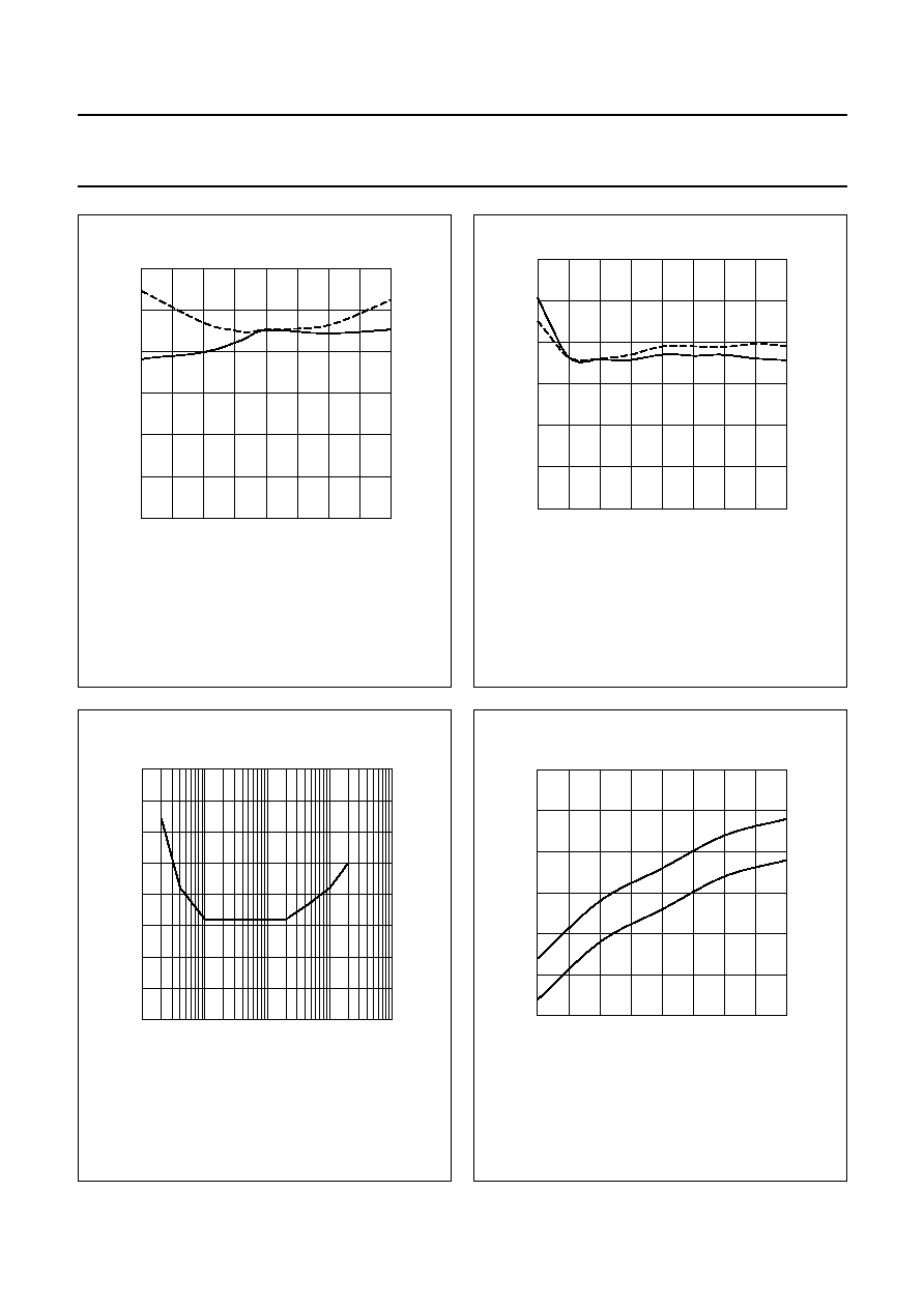
TYPICAL PERFORMANCE CHARACTERISTICS
Fig.10 Total power supply current as function of
junction temperature.
PECL outputs not connected
(1) V
CC
= 5.5 V.
(2) V
CC
= 3.0 V.
handbook, halfpage
-
40
0
40
120
50
20
10
40
MGR959
30
80
ICC
(mA)
Tj (
∞
C)
(2)
(1)
Fig.11 Differential output voltage as function of
junction temperature.
handbook, halfpage
1.40
1.16
1.32
1.36
MGR960
-
40
0
40
120
80
Tj (
∞
C)
1.28
1.24
1.20
Vo(dif)
(V)
V
o(dif)
= V
DOUT
-
V
DOUTQ
.
Fig.12 Differential output voltage as function of
differential input voltage.
handbook, halfpage
1
1.1
1.2
1.3
1.4
MGR961
10
-
3
10
-
2
10
-
1
1
10
Vi(dif)(p-p) (V)
Vo(dif)
(V)
V
o(dif)
= V
DOUT
-
V
DOUTQ
.
Fig.13 Differential output rise time and fall time as
function of differential input voltage.
handbook, halfpage
100
140
180
220
260
MGR962
t
(ps)
10
-
3
10
-
2
10
-
1
1
10
t r
t f
Vi(dif)(p-p) (V)

1999 Nov 03
14
Philips Semiconductors
Product specification
SDH/SONET STM4/OC12 and
1.25 Gbits/s Gigabit Ethernet postamplifiers
TZA3044; TZA3044B
Fig.14 Differential output rise time and fall time as
function of junction temperature.
handbook, halfpage
-
40
0
40
120
300
100
0
200
MGR963
80
t
(ps)
Tj (
∞
C)
t r
t f
Fig.15 Status detect level as function of I
RSET
.
V
i(dif)
= V
DIN
-
V
DINQ
.
(1) Input high threshold for 1 0 1 0 pattern (pin ST = HIGH).
(2) Input high threshold for 2
7
-
1 PRBS pattern (pin ST = HIGH).
(3) Input low threshold for 1 0 1 0 pattern (pin ST = LOW).
(4) Input low threshold for 2
7
-
1 PRBS pattern (pin ST = LOW).
handbook, halfpage
5
15
25
45
20
10
0
40
MGR964
50
30
35
IRSET (
µ
A)
(1)
(2)
(4)
(3)
Vi(dif)
(mV)
Fig.16 Status detect level as function of junction
temperature.
handbook, halfpage
-
40
0
40
120
20
10
0
30
MGR965
40
80
Tj (
∞
C)
Vi(dif)
(mV)
(1)
(2)
(3)
(4)
V
i(dif)
= V
DIN
-
V
DINQ
.
(1) Input high threshold for 1 0 1 0 pattern (pin ST = HIGH).
(2) Input high threshold for 2
7
-
1 PRBS pattern (pin ST = HIGH).
(3) Input low threshold for 1 0 1 0 pattern (pin ST = LOW).
(4) Input low threshold for 2
7
-
1 PRBS pattern (pin ST = LOW).
Fig.17 Status detect hysteresis as function of
I
RSET
.
(1) 1 0 1 0 pattern.
(2) 2
7
-
1 PRBS pattern.
handbook, halfpage
6
2
0
4
MGR966
5
15
25
45
35
IRSET (
µ
A)
hys
(dB)
(2)
(1)
1999 Nov 03
15
Philips Semiconductors
Product specification
SDH/SONET STM4/OC12 and
1.25 Gbits/s Gigabit Ethernet postamplifiers
TZA3044; TZA3044B
Fig.18 Status detect hysteresis as function of
junction temperature.
handbook, halfpage
-
40
0
40
120
4
2
1
3
MGR967
80
hys
(dB)
Tj (
∞
C)
(2)
(1)
(1) I
RSET
= 45
µ
A.
(2) I
RSET
= 10
µ
A.
Fig.19 Status detect ratio as function of I
RSET
.
where V
i(dif)
= input low threshold (pin ST = LOW).
(1) 2
7
-
1 PRBS pattern.
(2) 1 0 1 0 pattern.
Ratio
I
RSET
V
i dif
(
)
--------------
=
handbook, halfpage
0.003
0.001
0
0.002
MGR968
5
15
25
45
35
IRSET (
µ
A)
Ratio
(A/V)
(2)
(1)
Fig.20 Pulse Width Distortion (t
PWD
) as function of
differential input voltage.
handbook, halfpage
0
10
20
30
40
MGR969
10
-
3
10
-
2
10
-
1
1
10
tPWD
(ns)
Vi(dif)(p-p) (V)
Fig.21 V
RSET
as function of junction temperature.
handbook, halfpage
-
40
0
40
120
1.555
1.535
1.525
1.545
MGR970
80
Tj (
∞
C)
(2)
(1)
VRSET
(V)
V
RSET
= V
CCA
-
1.5 V.
(1) V
CC
= 5.5 V.
(2) V
CC
= 3.0 V.

1999 Nov 03
16
Philips Semiconductors
Product specification
SDH/SONET STM4/OC12 and
1.25 Gbits/s Gigabit Ethernet postamplifiers
TZA3044; TZA3044B
Fig.22 Differential output waveform with 4 mV differential input voltage.
handbook, full pagewidth
MGR956
200 mV/div
Fig.23 Differential output waveform with 2 V differential input voltage.
handbook, full pagewidth
MGR957
200 mV/div

1999 Nov 03
17
Philips Semiconductors
Product specification
SDH/SONET STM4/OC12 and
1.25 Gbits/s Gigabit Ethernet postamplifiers
TZA3044; TZA3044B
APPLICATION INFORMATION
Fig.24 Application diagram.
The numbers in brackets refer to the pad numbers of the bare die version.
handbook, full pagewidth
MGR251
(23) 12
DOUTQ
(24) 13
DOUT
1 k
50
50
1.5 nF
1.5 nF
100 nF
180 k
TZA3044
(1, 14)
1
(19, 20, 22, 25)
11
SUB
(16)
8
JAM
(17)
9
STQ
(18)
10
ST
(3, 4, 6, 9)
3
AGND
VCC
6
(11, 12)
VCCA
16
(30)
RSET
7
(13)
CF
15
(29)
Vref
14
(27, 28)
VCCD
DGND
data out
data in
level detect
status
VCC
-
2 V
5 (8)
DINQ
4 (7)
DIN
100 nF

1999
Nov
03
18
Philips Semiconductors
Product specification
SDH/SONET STM4/OC12 and
1.25 Gbits/s Gigabit Ether
net postamplifiers
TZA3044; TZA3044B
This text is here in white to force landscape pages to be rotated correctly when browsing through the pdf in the Acrobat reader.This text is here in
_
white to force landscape pages to be rotated correctly when browsing through the pdf in the Acrobat reader.This text is here inThis text is here in
white to force landscape pages to be rotated correctly when browsing through the pdf in the Acrobat reader. white to force landscape pages to be ...
g
ewidth
MGR252
(23) 12
DOUTQ
6
OUT
7
OUTQ
(24) 13
DOUT
1 k
50
50
1.5 nF
1.5 nF
100 nF
4 pF
1
µ
F
noise filter:
1-pole, 800 MHz
100
61 k
TZA3043T
TZA3044
(1, 14)
1
(19, 20, 22, 25)
11
SUB
(16)
8
JAM
(17)
9
STQ
(18)
10
ST
(3, 4, 6, 9)
3
AGND
8
VCC
VCC
6
(11, 12)
VCCA
16
(30)
RSET
7
(13)
CF
15
(29)
Vref
14
(27, 28)
VCCD
DGND
data out
level detect
status
VCC
-
2 V
5 (8)
DINQ
4 (7)
DIN
3
1
22 nF
680 nF
100 nF
(1)
(1)
(1)
2
GND
4
GND
5
GND
IPhoto
DREF
Fig.25 Gigabit Ethernet receiver using the TZA3043T and TZA3044.
(1) Ferrite bead e.g. Murata BLM10A700S.
The numbers in brackets refer to the pad numbers of the bare die version.

1999
Nov
03
19
Philips Semiconductors
Product specification
SDH/SONET STM4/OC12 and
1.25 Gbits/s Gigabit Ether
net postamplifiers
TZA3044; TZA3044B
This text is here in white to force landscape pages to be rotated correctly when browsing through the pdf in the Acrobat reader.This text is here in
_
white to force landscape pages to be rotated correctly when browsing through the pdf in the Acrobat reader.This text is here inThis text is here in
white to force landscape pages to be rotated correctly when browsing through the pdf in the Acrobat reader. white to force landscape pages to be ...
n
dbook, full pagewidth
MBK999
(23) 12
DOUTQ
6
OUT
7
OUTQ
(24) 13
DOUT
1 k
50
50
1.5 nF
1.5 nF
100 nF
8 pF
noise filter:
1-pole, 400 MHz
100
61 k
TZA3023T
TZA3044
(1, 14)
1
(19, 20, 22, 25)
11
SUB
(16)
8
JAM
(17)
9
STQ
(18)
10
ST
(3, 4, 6, 9)
3
AGND
8
VCC
VCC
6
(11, 12)
VCCA
16
(30)
RSET
7
(13)
CF
15
(29)
Vref
14
(27, 28)
VCCD
DGND
data out
level detect
status
VCC
-
2 V
5 (8)
DINQ
4 (7)
DIN
3
IPhoto
1
DREF
680 nF
100 nF
7.5
pF
1.1
pF
16.4 nH
16.4 nH
optional noise filter:
3-pole, 470 MHz Bessel
(1)
(1)
(1)
2
GND
4
GND
5
GND
Fig.26 STM4/OC12 receiver using the TZA3023T and TZA3044.
(1) Ferrite bead e.g. Murata BLM10A700S.
The numbers in brackets refer to the pad numbers of the bare die version.

1999 Nov 03
20
Philips Semiconductors
Product specification
SDH/SONET STM4/OC12 and
1.25 Gbits/s Gigabit Ethernet postamplifiers
TZA3044; TZA3044B
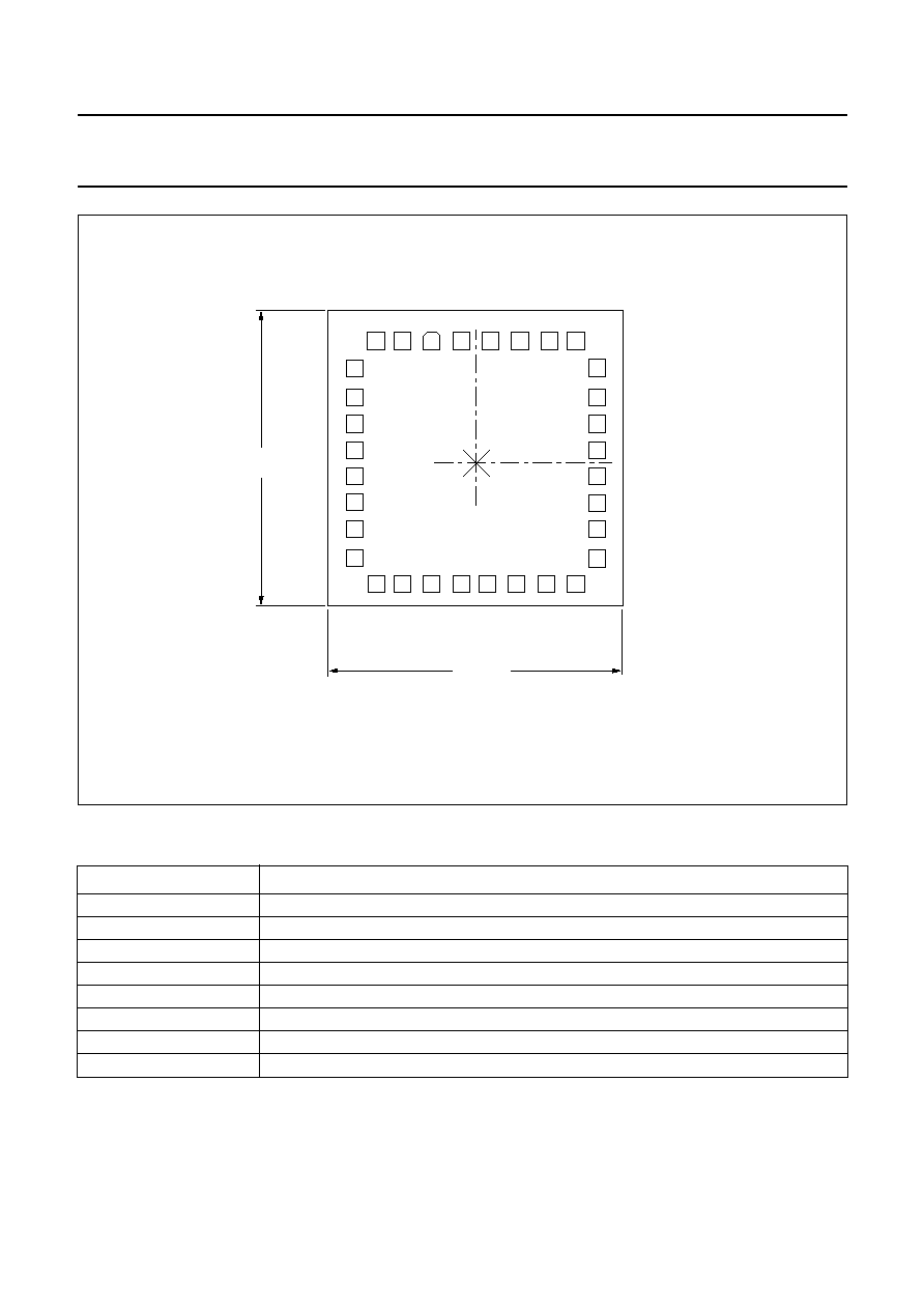
BONDING PADS
Note
1. The x and y coordinates represent the position of the
centre of the pad with respect to the centre of the die
(see Fig.27).
SYMBOL
PAD
COORDINATES
(1)
X
Y
SUB
1
-
235.7
+647.8
TEST
2
-
392.8
+647.8
AGND
3
-
532.8
+647.8
AGND
4
-
647.8
+507.1
n.c.
5
-
647.8
+350.0
AGND
6
-
647.8
+210.0
DIN
7
-
647.8
+70.0
DINQ
8
-
647.8
-
70.0
AGND
9
-
647.8
-
210.0
TEST
10
-
647.8
-
350.0
V
CCA
11
-
647.8
-
507.1
V
CCA
12
-
532.8
-
647.8
CF
13
-
392.8
-
647.8
SUB
14
-
235.7
-
647.8
TEST
15
-
78.6
-
647.8
JAM
16
+61.4
-
647.8
STQ
17
+218.5
-
647.8
ST
18
+375.6
-
647.8
DGND
19
+532.7
-
647.8
DGND
20
+647.8
-
507.1
TEST
21
+647.8
-
350.0
DGND
22
+647.8
-
210.0
DOUTQ
23
+647.8
-
70.0
DOUT
24
+647.8
+70.0
DGND
25
+647.8
+210.0
TEST
26
+647.8
+350.0
V
CCD
27
+647.8
+507.1
V
CCD
28
+532.7
+647.8
V
ref
29
+392.7
+647.8
RSET
30
+235.6
+647.8
n.c.
31
+78.5
+647.8
n.c.
32
-
78.6
+647.8
1999 Nov 03
21
Philips Semiconductors
Product specification
SDH/SONET STM4/OC12 and
1.25 Gbits/s Gigabit Ethernet postamplifiers
TZA3044; TZA3044B
Physical characteristics of bare die
PARAMETER
VALUE
Glass passivation
2.1
µ
m PSG (PhosphoSilicate Glass) on top of 0.65
µ
m oxynitride
Bonding pad dimension
minimum dimension of exposed metallization is 90
◊
90
µ
m (pad size = 100
◊
100
µ
m)
Metallization
1.22
µ
m W/AlCu/TiW
Thickness
380
µ
m nominal
Size
1.55
◊
1.55 mm (2.4 mm
2
)
Backing
silicon; electrically connected to GND potential through substrate contacts
Attache temperature
<440
∞
C; recommended die attache is glue
Attache time
<15 s
Fig.27 Bonding pad locations of TZA3044U and TZA3044BU.
handbook, full pagewidth
AGND
4
VCCD
27
TEST
26
DGND
25
DOUT
24
DOUTQ
23
DGND
22
TEST
21
DGND
20
AGND
6
DIN
7
DINQ
8
AGND
9
TEST
10
VCCA
11
n.c.
5
TZA3044U
TZA3044BU
12
V
CCA
3
A
GND
2
TEST
1
SUB
32
n.c.
31
n.c.
30
RSET
29
V
ref
28
V
CCD
13
CF
14
SUB
15
TEST
16
JA
M
17
STQ
18
ST
19
DGND
MGR242
1.55
(1)
mm
1.55
(1)
mm
x
y
0
0
(1) Typical value.

1999 Nov 03
22
Philips Semiconductors
Product specification
SDH/SONET STM4/OC12 and
1.25 Gbits/s Gigabit Ethernet postamplifiers
TZA3044; TZA3044B
PACKAGE OUTLINES
X
w
M
A
A
1
A
2
b
p
D
H
E
L
p
Q
detail X
E
Z
e
c
L
v
M
A
(A )
3
A
8
9
1
16
y
pin 1 index
UNIT
A
max.
A
1
A
2
A
3
b
p
c
D
(1)
E
(1)
(1)
e
H
E
L
L
p
Q
Z
y
w
v
REFERENCES
OUTLINE
VERSION
EUROPEAN
PROJECTION
ISSUE DATE
IEC
JEDEC
EIAJ
mm
inches
1.75
0.25
0.10
1.45
1.25
0.25
0.49
0.36
0.25
0.19
10.0
9.8
4.0
3.8
1.27
6.2
5.8
0.7
0.6
0.7
0.3
8
0
o
o
0.25
0.1
DIMENSIONS (inch dimensions are derived from the original mm dimensions)
Note
1. Plastic or metal protrusions of 0.15 mm maximum per side are not included.
1.0
0.4
SOT109-1
95-01-23
97-05-22
076E07S
MS-012AC
0.069
0.010
0.004
0.057
0.049
0.01
0.019
0.014
0.0100
0.0075
0.39
0.38
0.16
0.15
0.050
1.05
0.041
0.244
0.228
0.028
0.020
0.028
0.012
0.01
0.25
0.01
0.004
0.039
0.016
0
2.5
5 mm
scale
SO16: plastic small outline package; 16 leads; body width 3.9 mm
SOT109-1
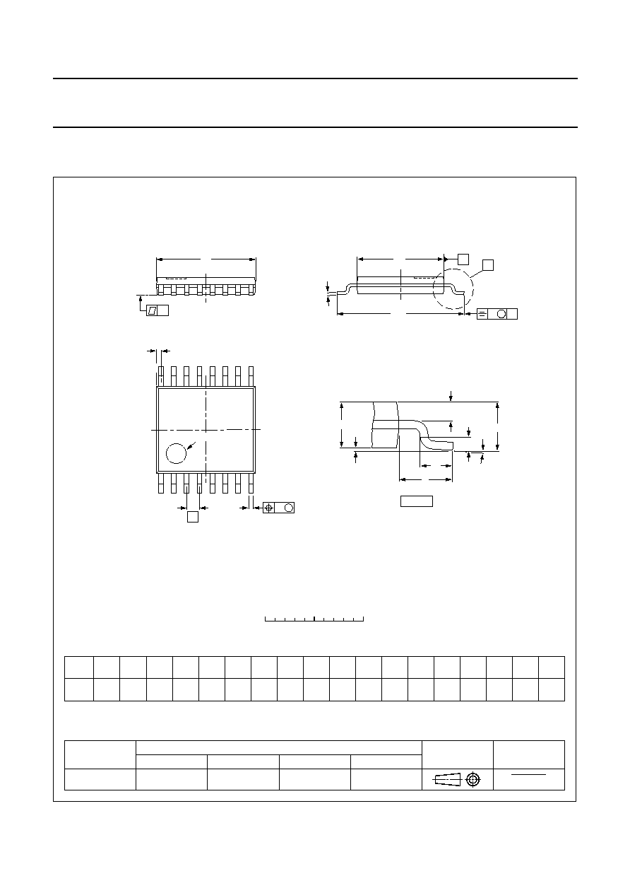
1999 Nov 03
23
Philips Semiconductors
Product specification
SDH/SONET STM4/OC12 and
1.25 Gbits/s Gigabit Ethernet postamplifiers
TZA3044; TZA3044B
UNIT
A
1
A
2
A
3
b
p
c
D
(1)
E
(2)
(1)
e
H
E
L
L
p
Q
Z
y
w
v
REFERENCES
OUTLINE
VERSION
EUROPEAN
PROJECTION
ISSUE DATE
IEC
JEDEC
EIAJ
mm
0.15
0.05
0.95
0.80
0.30
0.19
0.2
0.1
5.1
4.9
4.5
4.3
0.65
6.6
6.2
0.4
0.3
0.40
0.06
8
0
o
o
0.13
0.1
0.2
1.0
DIMENSIONS (mm are the original dimensions)
Notes
1. Plastic or metal protrusions of 0.15 mm maximum per side are not included.
2. Plastic interlead protrusions of 0.25 mm maximum per side are not included.
0.75
0.50
SOT403-1
MO-153
94-07-12
95-04-04
w
M
b
p
D
Z
e
0.25
1
8
16
9
A
A
1
A
2
L
p
Q
detail X
L
(A )
3
H
E
E
c
v
M
A
X
A
y
0
2.5
5 mm
scale
TSSOP16: plastic thin shrink small outline package; 16 leads; body width 4.4 mm
SOT403-1
A
max.
1.10
pin 1 index

1999 Nov 03
24
Philips Semiconductors
Product specification
SDH/SONET STM4/OC12 and
1.25 Gbits/s Gigabit Ethernet postamplifiers
TZA3044; TZA3044B
SOLDERING
Introduction to soldering surface mount packages
This text gives a very brief insight to a complex technology.
A more in-depth account of soldering ICs can be found in
our
"Data Handbook IC26; Integrated Circuit Packages"
(document order number 9398 652 90011).
There is no soldering method that is ideal for all surface
mount IC packages. Wave soldering is not always suitable
for surface mount ICs, or for printed-circuit boards with
high population densities. In these situations reflow
soldering is often used.
Reflow soldering
Reflow soldering requires solder paste (a suspension of
fine solder particles, flux and binding agent) to be applied
to the printed-circuit board by screen printing, stencilling or
pressure-syringe dispensing before package placement.
Several methods exist for reflowing; for example,
infrared/convection heating in a conveyor type oven.
Throughput times (preheating, soldering and cooling) vary
between 100 and 200 seconds depending on heating
method.
Typical reflow peak temperatures range from
215 to 250
∞
C. The top-surface temperature of the
packages should preferable be kept below 230
∞
C.
Wave soldering
Conventional single wave soldering is not recommended
for surface mount devices (SMDs) or printed-circuit boards
with a high component density, as solder bridging and
non-wetting can present major problems.
To overcome these problems the double-wave soldering
method was specifically developed.
If wave soldering is used the following conditions must be
observed for optimal results:
∑
Use a double-wave soldering method comprising a
turbulent wave with high upward pressure followed by a
smooth laminar wave.
∑
For packages with leads on two sides and a pitch (e):
≠ larger than or equal to 1.27 mm, the footprint
longitudinal axis is preferred to be parallel to the
transport direction of the printed-circuit board;
≠ smaller than 1.27 mm, the footprint longitudinal axis
must be parallel to the transport direction of the
printed-circuit board.
The footprint must incorporate solder thieves at the
downstream end.
∑
For packages with leads on four sides, the footprint must
be placed at a 45
∞
angle to the transport direction of the
printed-circuit board. The footprint must incorporate
solder thieves downstream and at the side corners.
During placement and before soldering, the package must
be fixed with a droplet of adhesive. The adhesive can be
applied by screen printing, pin transfer or syringe
dispensing. The package can be soldered after the
adhesive is cured.
Typical dwell time is 4 seconds at 250
∞
C.
A mildly-activated flux will eliminate the need for removal
of corrosive residues in most applications.
Manual soldering
Fix the component by first soldering two
diagonally-opposite end leads. Use a low voltage (24 V or
less) soldering iron applied to the flat part of the lead.
Contact time must be limited to 10 seconds at up to
300
∞
C.
When using a dedicated tool, all other leads can be
soldered in one operation within 2 to 5 seconds between
270 and 320
∞
C.

1999 Nov 03
25
Philips Semiconductors
Product specification
SDH/SONET STM4/OC12 and
1.25 Gbits/s Gigabit Ethernet postamplifiers
TZA3044; TZA3044B
Suitability of surface mount IC packages for wave and reflow soldering methods
Notes
1. All surface mount (SMD) packages are moisture sensitive. Depending upon the moisture content, the maximum
temperature (with respect to time) and body size of the package, there is a risk that internal or external package
cracks may occur due to vaporization of the moisture in them (the so called popcorn effect). For details, refer to the
Drypack information in the
"Data Handbook IC26; Integrated Circuit Packages; Section: Packing Methods".
2. These packages are not suitable for wave soldering as a solder joint between the printed-circuit board and heatsink
(at bottom version) can not be achieved, and as solder may stick to the heatsink (on top version).
3. If wave soldering is considered, then the package must be placed at a 45
∞
angle to the solder wave direction.
The package footprint must incorporate solder thieves downstream and at the side corners.
4. Wave soldering is only suitable for LQFP, TQFP and QFP packages with a pitch (e) equal to or larger than 0.8 mm;
it is definitely not suitable for packages with a pitch (e) equal to or smaller than 0.65 mm.
5. Wave soldering is only suitable for SSOP and TSSOP packages with a pitch (e) equal to or larger than 0.65 mm; it is
definitely not suitable for packages with a pitch (e) equal to or smaller than 0.5 mm.
PACKAGE
SOLDERING METHOD
WAVE
REFLOW
(1)
BGA, SQFP
not suitable
suitable
HLQFP, HSQFP, HSOP, HTSSOP, SMS
not suitable
(2)
suitable
PLCC
(3)
, SO, SOJ
suitable
suitable
LQFP, QFP, TQFP
not recommended
(3)(4)
suitable
SSOP, TSSOP, VSO
not recommended
(5)
suitable

1999 Nov 03
26
Philips Semiconductors
Product specification
SDH/SONET STM4/OC12 and
1.25 Gbits/s Gigabit Ethernet postamplifiers
TZA3044; TZA3044B
DEFINITIONS
LIFE SUPPORT APPLICATIONS
These products are not designed for use in life support appliances, devices, or systems where malfunction of these
products can reasonably be expected to result in personal injury. Philips customers using or selling these products for
use in such applications do so at their own risk and agree to fully indemnify Philips for any damages resulting from such
improper use or sale.
BARE DIE DISCLAIMER
All die are tested and are guaranteed to comply with all data sheet limits up to the point of wafer sawing for a period of
ninety (90) days from the date of Philips' delivery. If there are data sheet limits not guaranteed, these will be separately
indicated in the data sheet. There is no post waffle pack testing performed on individual die. Although the most modern
processes are utilized for wafer sawing and die pick and place into waffle pack carriers, Philips Semiconductors has no
control of third party procedures in the handling, packing or assembly of the die. Accordingly, Philips Semiconductors
assumes no liability for device functionality or performance of the die or systems after handling, packing or assembly of
the die. It is the responsibility of the customer to test and qualify their application in which the die is used.
Data sheet status
Objective specification
This data sheet contains target or goal specifications for product development.
Preliminary specification
This data sheet contains preliminary data; supplementary data may be published later.
Product specification
This data sheet contains final product specifications.
Limiting values
Limiting values given are in accordance with the Absolute Maximum Rating System (IEC 134). Stress above one or
more of the limiting values may cause permanent damage to the device. These are stress ratings only and operation
of the device at these or at any other conditions above those given in the Characteristics sections of the specification
is not implied. Exposure to limiting values for extended periods may affect device reliability.
Application information
Where application information is given, it is advisory and does not form part of the specification.

1999 Nov 03
27
Philips Semiconductors
Product specification
SDH/SONET STM4/OC12 and
1.25 Gbits/s Gigabit Ethernet postamplifiers
TZA3044; TZA3044B
NOTES

© Philips Electronics N.V.
SCA
All rights are reserved. Reproduction in whole or in part is prohibited without the prior written consent of the copyright owner.
The information presented in this document does not form part of any quotation or contract, is believed to be accurate and reliable and may be changed
without notice. No liability will be accepted by the publisher for any consequence of its use. Publication thereof does not convey nor imply any license
under patent- or other industrial or intellectual property rights.
Internet: http://www.semiconductors.philips.com
1999
68
Philips Semiconductors ≠ a worldwide company
For all other countries apply to: Philips Semiconductors,
International Marketing & Sales Communications, Building BE-p, P.O. Box 218,
5600 MD EINDHOVEN, The Netherlands, Fax. +31 40 27 24825
Argentina: see South America
Australia: 3 Figtree Drive, HOMEBUSH, NSW 2140,
Tel. +61 2 9704 8141, Fax. +61 2 9704 8139
Austria: Computerstr. 6, A-1101 WIEN, P.O. Box 213,
Tel. +43 1 60 101 1248, Fax. +43 1 60 101 1210
Belarus: Hotel Minsk Business Center, Bld. 3, r. 1211, Volodarski Str. 6,
220050 MINSK, Tel. +375 172 20 0733, Fax. +375 172 20 0773
Belgium: see The Netherlands
Brazil: see South America
Bulgaria: Philips Bulgaria Ltd., Energoproject, 15th floor,
51 James Bourchier Blvd., 1407 SOFIA,
Tel. +359 2 68 9211, Fax. +359 2 68 9102
Canada: PHILIPS SEMICONDUCTORS/COMPONENTS,
Tel. +1 800 234 7381, Fax. +1 800 943 0087
China/Hong Kong: 501 Hong Kong Industrial Technology Centre,
72 Tat Chee Avenue, Kowloon Tong, HONG KONG,
Tel. +852 2319 7888, Fax. +852 2319 7700
Colombia: see South America
Czech Republic: see Austria
Denmark: Sydhavnsgade 23, 1780 COPENHAGEN V,
Tel. +45 33 29 3333, Fax. +45 33 29 3905
Finland: Sinikalliontie 3, FIN-02630 ESPOO,
Tel. +358 9 615 800, Fax. +358 9 6158 0920
France: 51 Rue Carnot, BP317, 92156 SURESNES Cedex,
Tel. +33 1 4099 6161, Fax. +33 1 4099 6427
Germany: Hammerbrookstraþe 69, D-20097 HAMBURG,
Tel. +49 40 2353 60, Fax. +49 40 2353 6300
Hungary: see Austria
India: Philips INDIA Ltd, Band Box Building, 2nd floor,
254-D, Dr. Annie Besant Road, Worli, MUMBAI 400 025,
Tel. +91 22 493 8541, Fax. +91 22 493 0966
Indonesia: PT Philips Development Corporation, Semiconductors Division,
Gedung Philips, Jl. Buncit Raya Kav.99-100, JAKARTA 12510,
Tel. +62 21 794 0040 ext. 2501, Fax. +62 21 794 0080
Ireland: Newstead, Clonskeagh, DUBLIN 14,
Tel. +353 1 7640 000, Fax. +353 1 7640 200
Israel: RAPAC Electronics, 7 Kehilat Saloniki St, PO Box 18053,
TEL AVIV 61180, Tel. +972 3 645 0444, Fax. +972 3 649 1007
Italy: PHILIPS SEMICONDUCTORS, Via Casati, 23 - 20052 MONZA (MI),
Tel. +39 039 203 6838, Fax +39 039 203 6800
Japan: Philips Bldg 13-37, Kohnan 2-chome, Minato-ku,
TOKYO 108-8507, Tel. +81 3 3740 5130, Fax. +81 3 3740 5057
Korea: Philips House, 260-199 Itaewon-dong, Yongsan-ku, SEOUL,
Tel. +82 2 709 1412, Fax. +82 2 709 1415
Malaysia: No. 76 Jalan Universiti, 46200 PETALING JAYA, SELANGOR,
Tel. +60 3 750 5214, Fax. +60 3 757 4880
Mexico: 5900 Gateway East, Suite 200, EL PASO, TEXAS 79905,
Tel. +9-5 800 234 7381, Fax +9-5 800 943 0087
Middle East: see Italy
Netherlands: Postbus 90050, 5600 PB EINDHOVEN, Bldg. VB,
Tel. +31 40 27 82785, Fax. +31 40 27 88399
New Zealand: 2 Wagener Place, C.P.O. Box 1041, AUCKLAND,
Tel. +64 9 849 4160, Fax. +64 9 849 7811
Norway: Box 1, Manglerud 0612, OSLO,
Tel. +47 22 74 8000, Fax. +47 22 74 8341
Pakistan: see Singapore
Philippines: Philips Semiconductors Philippines Inc.,
106 Valero St. Salcedo Village, P.O. Box 2108 MCC, MAKATI,
Metro MANILA, Tel. +63 2 816 6380, Fax. +63 2 817 3474
Poland: Al.Jerozolimskie 195 B, 02-222 WARSAW,
Tel. +48 22 5710 000, Fax. +48 22 5710 001
Portugal: see Spain
Romania: see Italy
Russia: Philips Russia, Ul. Usatcheva 35A, 119048 MOSCOW,
Tel. +7 095 755 6918, Fax. +7 095 755 6919
Singapore: Lorong 1, Toa Payoh, SINGAPORE 319762,
Tel. +65 350 2538, Fax. +65 251 6500
Slovakia: see Austria
Slovenia: see Italy
South Africa: S.A. PHILIPS Pty Ltd., 195-215 Main Road Martindale,
2092 JOHANNESBURG, P.O. Box 58088 Newville 2114,
Tel. +27 11 471 5401, Fax. +27 11 471 5398
South America: Al. Vicente Pinzon, 173, 6th floor,
04547-130 S√O PAULO, SP, Brazil,
Tel. +55 11 821 2333, Fax. +55 11 821 2382
Spain: Balmes 22, 08007 BARCELONA,
Tel. +34 93 301 6312, Fax. +34 93 301 4107
Sweden: Kottbygatan 7, Akalla, S-16485 STOCKHOLM,
Tel. +46 8 5985 2000, Fax. +46 8 5985 2745
Switzerland: Allmendstrasse 140, CH-8027 ZÐRICH,
Tel. +41 1 488 2741 Fax. +41 1 488 3263
Taiwan: Philips Semiconductors, 6F, No. 96, Chien Kuo N. Rd., Sec. 1,
TAIPEI, Taiwan Tel. +886 2 2134 2886, Fax. +886 2 2134 2874
Thailand: PHILIPS ELECTRONICS (THAILAND) Ltd.,
209/2 Sanpavuth-Bangna Road Prakanong, BANGKOK 10260,
Tel. +66 2 745 4090, Fax. +66 2 398 0793
Turkey: Yukari Dudullu, Org. San. Blg., 2.Cad. Nr. 28 81260 Umraniye,
ISTANBUL, Tel. +90 216 522 1500, Fax. +90 216 522 1813
Ukraine: PHILIPS UKRAINE, 4 Patrice Lumumba str., Building B, Floor 7,
252042 KIEV, Tel. +380 44 264 2776, Fax. +380 44 268 0461
United Kingdom: Philips Semiconductors Ltd., 276 Bath Road, Hayes,
MIDDLESEX UB3 5BX, Tel. +44 208 730 5000, Fax. +44 208 754 8421
United States: 811 East Arques Avenue, SUNNYVALE, CA 94088-3409,
Tel. +1 800 234 7381, Fax. +1 800 943 0087
Uruguay: see South America
Vietnam: see Singapore
Yugoslavia: PHILIPS, Trg N. Pasica 5/v, 11000 BEOGRAD,
Tel. +381 11 62 5344, Fax.+381 11 63 5777
Printed in The Netherlands
465012/100/03/pp
28
Date of release:
1999 Nov 03
Document order number:
9397 750 06335