 | –≠–ª–µ–∫—Ç—Ä–æ–Ω–Ω—ã–π –∫–æ–º–ø–æ–Ω–µ–Ω—Ç: UAA2068G | –°–∫–∞—á–∞—Ç—å:  PDF PDF  ZIP ZIP |

DATA SHEET
Product specification
Supersedes data of 1998 Jan 07
File under Integrated Circuits, IC17
1998 Nov 19
INTEGRATED CIRCUITS
UAA2068G
Transmit chain and synthesizer with
integrated VCO for DECT

1998 Nov 19
2
Philips Semiconductors
Product specification
Transmit chain and synthesizer with
integrated VCO for DECT
UAA2068G
FEATURES
∑
Economical integrated solution for frequency generation
in DECT cordless telephones
∑
Integrated low phase noise 950 MHz VCO with
frequency doubler
∑
Local Oscillator (LO) drive (
-
14 dBm) for RF mixer
circuit
∑
Dedicated DECT PLL synthesizer
∑
3-line serial interface bus
∑
3 dBm output preamplifier with an integrated switch
∑
Low current consumption from 3 V supply
∑
Compatible with Philips Semiconductors ABC baseband
chip (PCD509x series).
APPLICATIONS
∑
1880 to 1920 MHz DECT cordless telephones.
GENERAL DESCRIPTION
The UAA2068G BiCMOS device integrates a 950 MHz
VCO, a frequency doubler, main and reference dividers
and a phase comparator, to implement a phase-locked
loop for DECT channel frequencies. The 1.9 GHz signal is
buffered and switched, in TX mode, to drive the transmit
power amplifier (CGY20xx series) or, in RX mode, to be
used as an LO signal for the receiver mixer IC (UAA2078).
The synthesizer's main divider is driven by the frequency
doubler output in the range from 1880 to 1920 MHz and
programmed via a 3-wire serial bus.
The reference divider ratio is fixed at 8. Outputs of the
main and reference dividers drive a phase comparator
where a charge pump produces phase error current pulses
for integration in an external loop filter. Only a passive loop
filter is necessary. The charge-pump current (phase
comparator gain) is set by an external resistor at pin R
SET
.
The VCO is powered from an internally regulated voltage
source and includes internal varicap diodes. Its tuning
range is wider than the required band to allow for
production spreads. In a TDMA system such as DECT, the
VCO and the synthesizer are switched on one slot before
the required one to lock the VCO to the required channel
frequency. Just before the required slot, the synthesizer is
switched off, allowing open-loop modulation of the VCO
during transmission. When opening the loop, the
frequency pulling (due to switching off the synthesizer) can
be maintained within the DECT specification.
The device is designed to operate from 3 NiCd cells in
pocket phones, with low current and nominal 3.6 V
supplies. Separate power and ground pins are provided to
the different parts of the circuit. The ground leads should
be short-circuited externally to prevent large currents
flowing across the die and thus causing damage.
All supply pins (V
CC
) must also be at the same potential,
except V
CC(CP)
which can be equal to or greater than the
other supply pins (e.g. V
CC
= 3 V and V
CC(CP)
= 5 V for
wider VCO control voltage range).
ORDERING INFORMATION
TYPE NUMBER
PACKAGE
NAME
DESCRIPTION
VERSION
UAA2068G
LQFP32
plastic low profile quad flat package; 32 leads; body 5
◊
5
◊
1.4 mm
SOT401-1
1998 Nov 19
3
Philips Semiconductors
Product specification
Transmit chain and synthesizer with
integrated VCO for DECT
UAA2068G
QUICK REFERENCE DATA
V
CC
= 3.6 V; V
CC(CP)
= 3.6 V; T
amb
= 25
∞
C; unless otherwise specified. Characteristics for which only a typical value is
given are not tested.
SYMBOL
PARAMETER
CONDITIONS
MIN.
TYP.
MAX.
UNIT
V
CC
general supply voltage
3.0
3.6
5.2
V
V
CC(CP)
charge-pump supply voltage
V
CC(CP)
V
CC
3.0
3.6
5.2
V
I
CC(SYA)
+
I
CC(SYD)
synthesizer supply current
S_EN = 1
-
9.5
14
mA
I
CC(VCO)
+
I
CC(BUF)
VCO and buffer parts supply current
VCO_ON = 1
-
9.5
14
mA
I
CC(DBL)
doubler supply current
in RX mode
-
14.4
19
mA
in TX mode
-
10
14
mA
I
CC(AMP)
TX preamplifier supply current
in RX mode
-
0
50
µ
A
in TX mode
-
24
32
mA
I
CC(pd)
total supply current in power-down mode
-
5
50
µ
A
f
o(RF)
RF output frequency
1880
-
1920
MHz
f
xtal
crystal reference input frequency
-
13.824
-
MHz
f
PC
phase comparator frequency
-
1728
-
kHz
T
amb
operating ambient temperature
-
10
-
+60
∞
C

1998 Nov 19
4
Philips Semiconductors
Product specification
Transmit chain and synthesizer with
integrated VCO for DECT
UAA2068G
BLOCK DIAGRAM
Fig.1 Block diagram.
handbook, full pagewidth
MGK383
RF
SWITCH
DOUBLER
3-LINE BUS
PHASE
COMPARATOR
CHARGE
PUMP
MAIN DIVIDER
REFERENCE DIVIDER
PREAMP
T_EN
LO
BUFFER
BUFFER
UAA2068G
VCO
CPGND
CP
VCO_ON
VCC(AMP)
VMOD
VCOA
VREG
VCGND
VCOB
VTUNE
VCOGND
VCC(CP)
RSET
RSET
VCC(DBL)
VCC(VCO)
VCC(DBL)
DBLGND
VCC(BUF)
L
L
SYDGND
XTAL
VCC(SYD)
VCC(SYA)
SYAGND
R_OFF
AMPGND
TXB
30
15
11
16
17
24
21
20
23
18
25
22
32
5
2
13
12
27
28
29
26
1
31
4
3
6
10
7
19
14
9
8
TXA
CLK
DATA
S_EN
LOA
LOB

1998 Nov 19
5
Philips Semiconductors
Product specification
Transmit chain and synthesizer with
integrated VCO for DECT
UAA2068G
PINNING
Notes
1. Pins 19 and 22 are internally short-circuited.
2. Use with S_PWR on ABC baseband chip.
3. Use with R_PWR on ABC baseband chip.
SYMBOL
PIN
DESCRIPTION
DATA
1
3-wire programming bus data input
V
CC(SYD)
2
synthesizer CMOS divider positive supply voltage
SYDGND
3
synthesizer CMOS divider ground
XTAL
4
reference frequency input
V
CC(SYA)
5
synthesizer prescaler positive supply voltage
SYAGND
6
synthesizer prescaler ground
CPGND
7
charge-pump ground
CP
8
charge-pump output signal
V
CC(CP)
9
charge-pump positive supply voltage
R
SET
10
charge-pump current setting input
V
CC(DBL)
11
doubler positive supply voltage
LOA
12
local oscillator output A
LOB
13
local oscillator output B
DBLGND
14
doubler ground
T_EN
15
transmit enable signal input
V
CC(BUF)
16
VCO isolation buffer positive supply voltage
V
CC(VCO)
17
VCO positive supply voltage
V
MOD
18
transmit modulation input
VCOGND
19
VCO ground; note 1
VCOA
20
VCO inductor connection A
VCOB
21
VCO inductor connection B
VCGND
22
internal varicap ground; note 1
V
TUNE
23
VCO tuning input
V
REG
24
VCO regulator output
VCO_ON
25
VCO power on control input; note 2
R_OFF
26
power on control for RX LO buffer/TX preamplifier; note 3
AMPGND
27
transmit amplifier ground
TXB
28
transmit amplifier output B
TXA
29
transmit amplifier output A
V
CC(AMP)
30
transmit amplifier positive supply voltage
CLK
31
3-wire programming bus clock input
S_EN
32
synthesizer enable signal input

1998 Nov 19
6
Philips Semiconductors
Product specification
Transmit chain and synthesizer with
integrated VCO for DECT
UAA2068G
Fig.2 Pin configuration.
handbook, full pagewidth
UAA2068G
MGK382
1
2
3
4
5
6
7
8
24
23
22
21
20
19
18
17
9
10
11
12
13
14
15
16
32
31
30
29
28
27
26
25
DATA
VCC(SYD)
SYDGND
XTAL
VCC(SYA)
SYAGND
CPGND
CP
VCO_ON
R_OFF
AMPGND
TXB
TXA
V
CC(AMP)
CLK
S_EN
VCC(VCO)
VMOD
VCOA
VREG
VCGND
VCOB
VTUNE
VCOGND
V
CC(CP)
R
SET
V
CC(DBL)
LOA
DBLGND
T_EN
V
CC(BUF)
LOB
FUNCTIONAL DESCRIPTION
Transmit chain
VCO,
BUFFER AND FREQUENCY DOUBLER
The VCO operates at a nominal centre frequency of
950 MHz. It is fully integrated apart from two inductors
which complete the resonator network. This VCO operates
from an on-chip regulated power supply (V
REG
), which
minimizes frequency disturbances due to variations in
supply voltage. The buffered VCO signal is fed into a
frequency doubler. The large difference between the
transmitted and VCO frequencies reduces
transmitter-oscillator coupling problems.
The output of the doubler is used to drive the synthesizer
main divider and can also be switched to either the TX
preamplifier or the RX LO output buffer. The high isolation
obtained from the VCO buffer and the frequency doubler
ensures very small frequency changes when turning on
the TX preamplifier or the RX LO output buffer. In TX
mode, the oscillator can be directly modulated with GMSK
filtered data at pin V
MOD
.
RF
SWITCH
The RF switch passes the doubled VCO signal to either
the TX preamplifier (when T_EN is HIGH) or to the RX LO
buffer (when T_EN is LOW). In TX mode, the difference in
the RF power levels, observed at the TX output when
T_EN is switched from LOW-to-HIGH, is typically 40 dB.
TX
PREAMPLIFIER
The TX preamplifier amplifies the RF signal up to a level of
3 dBm which is suitable for use with Philips
Semiconductors DECT power amplifiers such as the
CGY20xx series. It is powered-up when both R_OFF and
VCO_ON are HIGH.
RX LO
BUFFER
The RX LO buffer outputs the frequency doubled VCO
signal at a level of
-
14 dBm. This signal can then be used
as the local oscillator drive for the receive mixers of
devices such as the UAA2078. The buffer is powered-up
when R_OFF is LOW and VCO_ON is HIGH.

1998 Nov 19
7
Philips Semiconductors
Product specification
Transmit chain and synthesizer with
integrated VCO for DECT
UAA2068G
Synthesizer
M
AIN DIVIDER
The main divider is clocked by the RF signal from the
internal frequency doubler. The divider operates at
frequencies from 1880 to 1920 MHz. It consists of a
bipolar prescaler followed by a CMOS counter. Any main
divider ratio from 1024 to 1151 inclusive can be
programmed.
R
EFERENCE DIVIDER
The reference divider is clocked by the signal at pin XTAL.
The circuit operates with levels from 50 to 500 mV (RMS)
at a frequency of 13.824 MHz, with a fixed divider ratio
of 8.
P
HASE COMPARATOR
The phase comparator is driven by the output of the main
and reference dividers. It produces current pulses at
pin CP. The pulse duration is equal to the difference in
time of arrival of the edges from the two dividers. If the
main divider edge arrives first, CP sinks current. If the
reference divider edge arrives first, CP sources current.
The DC value of the charge-pump current is nominally ten
times the current drawn by the external resistor connected
to pin R
SET
. Additional circuitry is included to ensure that
the gain of the phase detector remains linear even for
small phase errors.
The charge pump has a separate supply, V
CC(CP)
, which
helps to reduce the interference on the charge-pump
output from other parts of the circuit. V
CC(CP)
can be higher
than the other supply voltages if a wider range on the VCO
input is required. The V
CC(CP)
voltage must not be less
than that on other V
CC
pins.
Serial programming bus
A simple 3-line unidirectional serial bus is used to program
the circuit. These 3 lines are data (DATA), clock (CLK) and
enable (S_EN). The data sent to the device is loaded in
bursts framed by S_EN. Programming clock edges and
their appropriate data bits are ignored until S_EN goes
active LOW. The programmed information is read directly
by the main divider when S_EN returns HIGH. During
synthesizer operation, S_EN should be kept HIGH.
In normal operating mode, only the last 8 bits serially
clocked into the device are retained within the register.
Additional leading bits are ignored, and no check is made
on the number of clock pulses. The data format is shown
in Table 2. The first bit entered is b7, the last bit is b0.
For the divider ratio, the first bit (b6) entered is the most
significant (MSB).
S_EN must be LOW to capture new programming data.
S_EN must be HIGH to switch on the synthesizer.
Operating modes
The synthesizer is on when the input signal S_EN is HIGH,
and off when S_EN is LOW. When turned on, the dividers
and phase detector are synchronized to avoid a random
initial phase error. When turned off, the phase detector is
synchronized with the dividers to avoid interrupting a
charge-pump pulse.
The VCO is on when the input signal VCO_ON is HIGH.
The polarity of VCO_ON is chosen for compatibility with
output S_PWR at the ABC chip. When turned on, it needs
some time (typically 30
µ
s) to reach its steady state.
The TX preamplifier is on when both R_OFF and VCO_ON
are HIGH. The polarity of R_OFF is chosen for
compatibility with output R_PWR at the ABC chip. When
turned on, it needs some time (typically 10
µ
s) to reach its
steady state. In transmit mode, the timing of the R_OFF
LOW-to-HIGH transition can be chosen such that the TX
preamplifier is turned on while the synthesizer loop
remains closed thus avoiding frequency pulling of the
VCO. In the receive mode, depending on the exact timing
of R_OFF compared to VCO_ON, the TX preamplifier can
be switched on at the beginning of the previous slot, but is
switched off when the R_OFF goes LOW; this occurs
when the synthesizer loop is closed. The LO output
amplifier is turned on when R_OFF is LOW and VCO_ON
is HIGH.
The UAA2068G has a very low current consumption in
power-down mode.

1998 Nov 19
8
Philips Semiconductors
Product specification
Transmit chain and synthesizer with
integrated VCO for DECT
UAA2068G
Table 1
Mode control; note 1
Notes
1. X = don't care.
2. PLL blocks are the main divider, reference divider, phase detector and charge pump.
3. A reference signal is needed on pin XTAL for correct operation.
BLOCK STATUS
VCO_ON
R_OFF
T_EN
S_EN
VCO, buffer, doubler, RF switch, TX preamplifier and LO buffer
powered-down
0
X
X
X
VCO, buffer, doubler, RF switch and TX preamplifier powered-up
1
1
1
X
LO buffer powered-down
Nominal RF signal at TX output
VCO, buffer, doubler, RF switch and TX preamplifier powered-up
1
1
0
X
LO buffer powered-down
No RF signal output
VCO, buffer, doubler, RF switch and LO buffer powered-up
1
0
0
X
TX preamplifier powered-down
Nominal RF signal at LO buffer output
VCO, buffer, doubler, RF switch and LO buffer powered-up
1
0
1
X
TX preamplifier powered-down
No RF signal output
To power-down PLL blocks; notes 2 and 3
1
X
X
0
To power-up PLL blocks; notes 2 and 3
1
X
X
1
All blocks in power-down state; notes 2 and 3
0
X
X
0
New PLL division ratio is loaded and the PLL blocks are powered-up
on the rising edge of S_EN; note 3
1
X
X
0 to 1
1998 Nov 19
9
Philips Semiconductors
Product specification
Transmit chain and synthesizer with
integrated VCO for DECT
UAA2068G
Table 2
Bit allocation; notes 1 and 2
Notes
1. X = don't care.
2. In normal operation, only 8 bits are programmed into the register.
3. For normal operation, b15 to b8 do not need to be programmed.
4. The validation bit (b7) must be programmed with zero for normal operation.
5. Bit b6 is the MSB of the main divider coefficient.
6. The main divider ratio is equal to 1024 plus the programmed value (see Table 3).
Table 3
Main divider programming
LIMITING VALUES
In accordance with the Absolute Maximum Rating System (IEC 134).
Note
1. Pins short-circuited internally must be short-circuited externally.
HANDLING
Inputs and outputs are protected against electrostatic discharge in normal handling. However, to be totally safe, it is
desirable to take normal precautions appropriate to handling MOS devices.
FIRST
IN
REGISTER BIT ALLOCATION
LAST
IN
DATA FIELD
b15
(3)
b14
(3)
b13
(3)
b12
(3)
b11
(3)
b10
(3)
b9
(3)
b8
(3)
b7
(4)
b6
(5)
b5
b4
b3
b2
b1
b0
X
X
X
X
X
X
X
X
0
main divider programming
(6)
b6
b5
b4
b3
b2
b1
b0
MAIN DIVIDER
RATIO
SYNTHESIZED
FREQUENCY (MHz)
Binary equivalent of n
1024 + n
1.728
◊
(1024 + n)
1
0
0
0
0
0
1
1089
1881.792
1
0
0
1
0
1
0
1098
1897.344
SYMBOL
PARAMETER
CONDITIONS
MIN.
MAX.
UNIT
V
CC
supply voltage
-
0.3
+5.5
V
V
CC(CP)
charge-pump supply voltage
-
0.3
+5.5
V
V
CC(CP)
-
V
CC
difference in voltage between V
CC(CP)
and V
CC
-
0.3
+5.5
V
GND
difference in ground supply voltage applied
between all ground pins
note 1
-
0.3
V
P
tot
total power dissipation
-
275
mW
T
stg
storage temperature
-
55
+125
∞
C
T
amb
operating ambient temperature
-
10
+60
∞
C
T
j
junction temperature
-
150
∞
C

1998 Nov 19
10
Philips Semiconductors
Product specification
Transmit chain and synthesizer with
integrated VCO for DECT
UAA2068G
THERMAL CHARACTERISTICS
CHARACTERISTICS
V
CC
= 3.6 V; V
CC(CP)
= 3.6 V; T
amb
= 25
∞
C; unless otherwise specified. Characteristics for which only a typical value is
given are not tested.
SYMBOL
PARAMETER
CONDITIONS
VALUE
UNIT
R
th(j-a)
thermal resistance from junction to ambient
in free air
100
K/W
SYMBOL
PARAMETER
CONDITIONS
MIN.
TYP.
MAX.
UNIT
Supplies
V
CC
supply voltage
3
3.6
5.2
V
V
CC(CP)
charge-pump supply voltage
V
CC(CP)
V
CC
3
3.6
5.2
V
I
CC(SYA)
+
I
CC(SYD)
synthesizer supply current
S_EN = 1
-
9.5
14
mA
I
CC(VCO)
+
I
CC(BUF)
VCO and buffer parts supply
current
VCO_ON = 1
-
9.5
14
mA
I
CC(DBL)
doubler supply current
in RX mode
-
14.4
19
mA
in TX mode
-
10
14
mA
I
CC(AMP)
TX preamplifier supply current
in RX mode
-
0
50
µ
A
in TX mode
-
24
32
mA
I
CC(pd)
total supply current in
power-down mode
-
5
50
µ
A
Synthesizer main divider
f
RF
RF frequency
1880
-
1920
MHz
R
m
main divider ratio
1024
-
1151
Synthesizer reference divider input
f
xtal
crystal reference input frequency
-
13.824
-
MHz
V
xtal(rms)
sinusoidal input signal level
(RMS value)
50
-
500
mV
R
ref
reference division ratio
-
8
-
R
i
input resistance (real part of the
input impedance)
f
xtal
= 13.824 MHz
-
4.5
-
k
C
i
input capacitance (imaginary
part of the input impedance)
-
2.5
-
pF
Phase detector
f
PC
phase comparator frequency
-
1728
-
kHz
Charge-pump output
I
o(cp)
charge-pump output current
V
CP
=
1
/
2
V
CC
;
R
SET
= 8.2 k
-
1.5
-
mA
I
o(cp)(err)
charge-pump output current error note 1
-
25
-
+25
%
I
match
sink-to-source current matching
V
CP
=
1
/
2
V
CC
-
±
5
-
%
I
L(cp)
charge-pump-off leakage current
V
CP
=
1
/
2
V
CC
-
1
0
+1
nA
1998 Nov 19
11
Philips Semiconductors
Product specification
Transmit chain and synthesizer with
integrated VCO for DECT
UAA2068G
Charge-pump current setting resistor input; pin R
SET
R
SET
external resistor connected
between pin R
SET
and ground
5.6
-
12
k
V
SET
regulated voltage at pin R
SET
-
1.2
-
V
VCO
f
VCO
oscillator frequency
over full temperature
range; note 2
940
-
960
MHz
G
VCO
tuning input VCO gain
-
45
-
MHz/V
G
MOD
modulation input VCO gain
-
1
-
MHz/V
Switch part
FTLO
TXoff
isolation between LO and TX
outputs when TX preamplifier is
off (RX mode)
f = 1890 MHz; note 2
-
-
50
-
dB
FTLO
TXon
isolation due to the switch when
TX preamplifier is on (TX mode)
f = 1890 MHz; note 2
-
-
40
-
dB
TX preamplifier and LO buffer parts
P
o(TX)
TX preamplifier output power
over full temperature
range; note 2
0
3
7
dBm
f
o(TX)
output frequency on TX
preamplifier or LO buffer
1880
-
1920
MHz
R
o(TX)
TX preamplifier output resistance
(real part of the parallel output
impedance)
balanced
-
150
-
C
o(TX)
TX preamplifier output
capacitance (imaginary part of
the parallel output impedance)
balanced
-
0.5
-
pF
FTVCO
TX
VCO frequency feedthrough at
the TX output
referenced to the f
o(TX)
level; note 2
-
-
41
-
36
dBc
CNR
25
carrier-to-noise ratio at TX output
carrier offset
f = 25 kHz
-
-
75
-
dBc/Hz
CNR
4686
carrier-to-noise ratio at TX output
carrier offset
f = 4686 kHz
-
-
135
-
132
dBc/Hz
f
o(offset)
total frequency shift due to
note 2
-
-
±
15
kHz
200 mV V
CC
change
disabling the synthesizer
measured 20
µ
s after
disabling the synthesizer
f
o(drift)
frequency drift during a slot
note 2
-
1
±
10
kHz
P
o(LO)
LO preamplifier output power
note 2
-
-
14
-
dBm
R
o(LO)
LO preamplifier output
resistance (real part of the
parallel output impedance)
balanced
-
120
-
C
o(LO)
LO preamplifier output
capacitance (imaginary part of
the parallel output impedance)
balanced
-
0
-
pF
SYMBOL
PARAMETER
CONDITIONS
MIN.
TYP.
MAX.
UNIT
1998 Nov 19
12
Philips Semiconductors
Product specification
Transmit chain and synthesizer with
integrated VCO for DECT
UAA2068G
Notes
1. Condition: 0.5 < V
CP
< (V
CC(CP)
-
0.5).
2. Measured and guaranteed only on the Philips evaluation board, including PCB and balun filter.
3. V
IH
should never exceed 5.2 V.
SERIAL BUS TIMING CHARACTERISTICS
V
CC
= 3.6 V; T
amb
= 25
∞
C; unless otherwise specified.
Interface logic input signal levels; pins DATA, CLK, S_EN, T_EN, R_OFF and VCO_ON
V
IH
HIGH-level input voltage
note 3
2.2
-
V
CC
+ 0.3
V
V
IL
LOW-level input voltage
-
0.3
-
+0.5
V
I
bias
input bias current
logic 1 or logic 0
-
5
-
+5
µ
A
C
i
input capacitance
-
2
-
pF
SYMBOL
PARAMETER
MIN.
TYP.
MAX.
UNIT
Serial programming clock; CLK
t
r
input rise time
-
10
40
ns
t
f
input fall time
-
10
40
ns
T
cy
clock period
100
-
-
ns
Enable programming; S_EN
t
START
delay to rising clock edge
40
-
-
ns
t
END
delay from last falling clock edge
-
20
-
-
ns
t
W
minimum inactive pulse width
4000
-
-
ns
t
SU;S_EN
enable set-up time to next clock edge
20
-
-
ns
Register serial input data; DATA
t
SU;DAT
input data to clock set-up time
20
-
-
ns
t
HD;DAT
input data to clock hold time
20
-
-
ns
SYMBOL
PARAMETER
CONDITIONS
MIN.
TYP.
MAX.
UNIT
Fig.3 Serial bus timing diagram.
handbook, full pagewidth
MBK095
MSB
LSB
tSTART
tSU;DAT
tHD;DAT
Tcy
tr
tf
tW
tEND
tSU;S_EN
CLK
DATA
S_EN

1998 Nov 19
13
Philips Semiconductors
Product specification
Transmit chain and synthesizer with
integrated VCO for DECT
UAA2068G
TIMING CHARACTERISTICS
Fig.4 Application bus timing diagram.
(1) On ABC baseband chip.
handbook, full pagewidth
MGK384
slot time
previous slot
active slot
DATA
CLK
S_EN
VCO_ON
= S_PWR
(1)
R_OFF
= R_PWR
(1)
T_EN
DATA
In RX mode
In TX mode
CLK
S_EN
VCO_ON
= S_PWR
(1)
R_OFF
= R_PWR
(1)
T_EN

1998 Nov 19
14
Philips Semiconductors
Product specification
Transmit chain and synthesizer with
integrated VCO for DECT
UAA2068G
APPLICATION INFORMATION
Fig.5 Typical application diagram.
L1 and L2: order of magnitude.
Values depend on board layout.
handbook, full pagewidth
1 k
1 k
1 k
L1
6.8 nH
L2
6.8 nH
1 k
1 k
1.5 k
3.9 k
8.2 k
1 k
UAA2068G
MGK385
1
2
32
31
30
29
TXOUT
28
27
26
25
9
10
11
12
13
14
15
16
RSET
3
from
ABC
chip
4
5
6
7
8
24
from ABC
chip
from
ABC chip
8.2 nH
1.8 nH
3.9 pF
6.8 nH
6.8 nH
8.2 nH
8.2 pF
8.2 pF
100 nF
8.2 pF
8.2 pF
22 pF
22 pF
8.2 pF
8.2 pF
8.2
pF
82 nF
8.2 pF
8.2 nF
120 pF
8.2 pF
8.2
pF
8.2
pF
8.2
pF
8.2 pF
8.2 pF
8.2 pF
1 pF
1 pF
10 pF
10 pF
from ABC chip
to receiver
loop filter
NPO
560 pF
23
22
21
20
19
18
17
DATA
VCC(SYD)
VCC
SYDGND
XTAL
VCC(SYA)
SYAGND
CPGND
CP
VCO_ON
R_OFF
AMPGND
TXB
TXA
V
CC(AMP)
CLK
S_EN
VCC(VCO)
VMOD
VCOA
VREG
VCGND
VCOB
VTUNE
VCOGND
V
CC(CP)
R
SET
V
CC(DBL)
LOA
DBLGND
T_EN
V
CC(BUF)
LOB
VCC
VCC
VCC
VCC
VCC
1998 Nov 19
15
Philips Semiconductors
Product specification
Transmit chain and synthesizer with
integrated VCO for DECT
UAA2068G
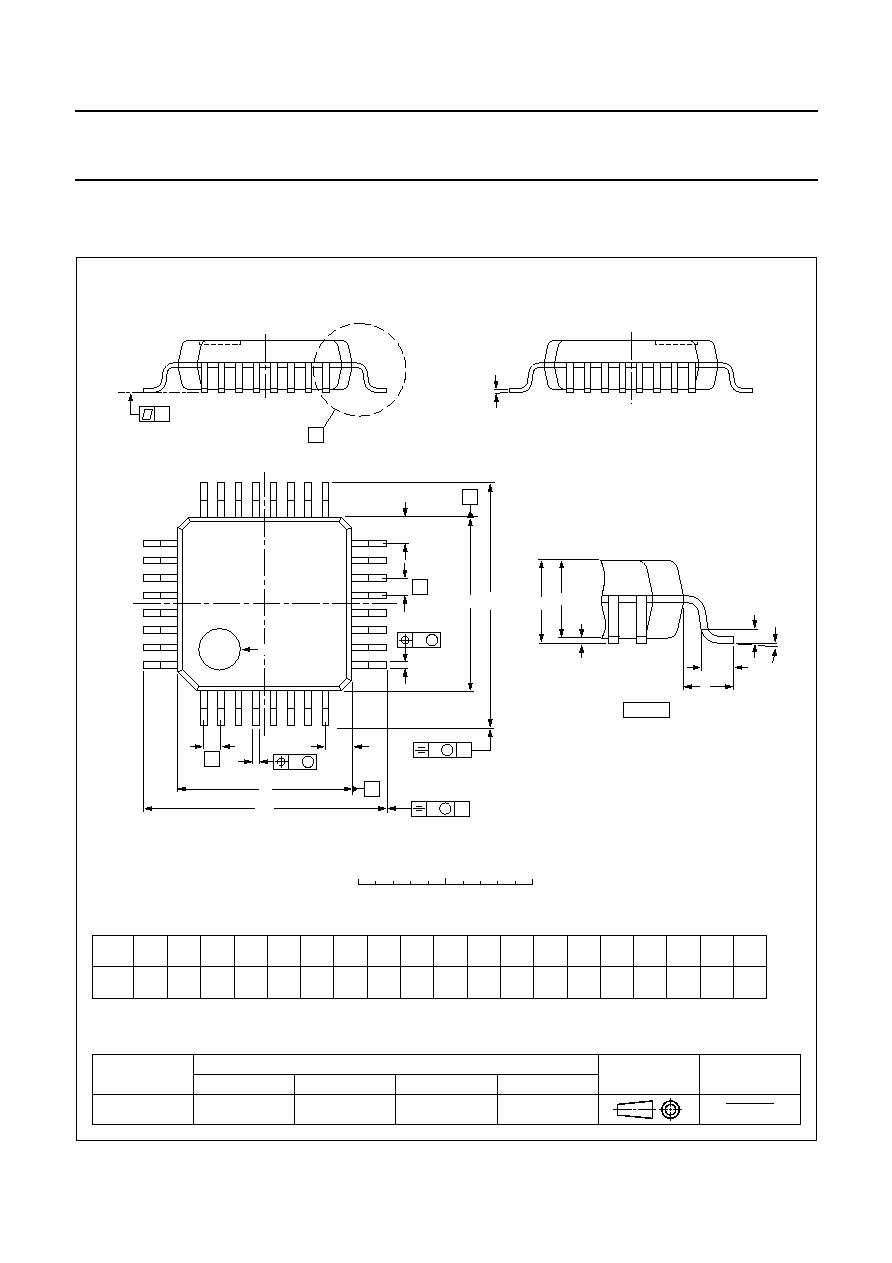
PACKAGE OUTLINE
0.2
UNIT
A
max.
A
1
A
2
A
3
b
p
c
E
(1)
e
H
E
L
L
p
Z
y
w
v
REFERENCES
OUTLINE
VERSION
EUROPEAN
PROJECTION
ISSUE DATE
IEC
JEDEC
EIAJ
mm
1.60
0.15
0.05
1.5
1.3
0.25
0.27
0.17
0.18
0.12
5.1
4.9
0.5
7.15
6.85
1.0
0.95
0.55
7
0
o
o
0.12
0.1
DIMENSIONS (mm are the original dimensions)
Note
1. Plastic or metal protrusions of 0.25 mm maximum per side are not included.
0.75
0.45
SOT401-1
95-12-19
97-08-04
D
(1)
(1)
(1)
5.1
4.9
H
D
7.15
6.85
E
Z
0.95
0.55
D
b
p
e
E
B
8
D
H
b
p
E
H
v
M
B
D
ZD
A
Z E
e
v
M
A
X
1
32
25
24
17
16
9
A
1
A
L
p
detail X
L
(A )
3
A
2
y
w
M
w
M
0
2.5
5 mm
scale
LQFP32: plastic low profile quad flat package; 32 leads; body 5 x 5 x 1.4 mm
SOT401-1
c
pin 1 index

1998 Nov 19
16
Philips Semiconductors
Product specification
Transmit chain and synthesizer with
integrated VCO for DECT
UAA2068G
SOLDERING
Introduction to soldering surface mount packages
This text gives a very brief insight to a complex technology.
A more in-depth account of soldering ICs can be found in
our
"Data Handbook IC26; Integrated Circuit Packages"
(document order number 9398 652 90011).
There is no soldering method that is ideal for all surface
mount IC packages. Wave soldering is not always suitable
for surface mount ICs, or for printed-circuit boards with
high population densities. In these situations reflow
soldering is often used.
Reflow soldering
Reflow soldering requires solder paste (a suspension of
fine solder particles, flux and binding agent) to be applied
to the printed-circuit board by screen printing, stencilling or
pressure-syringe dispensing before package placement.
Several methods exist for reflowing; for example,
infrared/convection heating in a conveyor type oven.
Throughput times (preheating, soldering and cooling) vary
between 100 and 200 seconds depending on heating
method.
Typical reflow peak temperatures range from
215 to 250
∞
C. The top-surface temperature of the
packages should preferable be kept below 230
∞
C.
Wave soldering
Conventional single wave soldering is not recommended
for surface mount devices (SMDs) or printed-circuit boards
with a high component density, as solder bridging and
non-wetting can present major problems.
To overcome these problems the double-wave soldering
method was specifically developed.
If wave soldering is used the following conditions must be
observed for optimal results:
∑
Use a double-wave soldering method comprising a
turbulent wave with high upward pressure followed by a
smooth laminar wave.
∑
For packages with leads on two sides and a pitch (e):
≠ larger than or equal to 1.27 mm, the footprint
longitudinal axis is preferred to be parallel to the
transport direction of the printed-circuit board;
≠ smaller than 1.27 mm, the footprint longitudinal axis
must be parallel to the transport direction of the
printed-circuit board.
The footprint must incorporate solder thieves at the
downstream end.
∑
For packages with leads on four sides, the footprint must
be placed at a 45
∞
angle to the transport direction of the
printed-circuit board. The footprint must incorporate
solder thieves downstream and at the side corners.
During placement and before soldering, the package must
be fixed with a droplet of adhesive. The adhesive can be
applied by screen printing, pin transfer or syringe
dispensing. The package can be soldered after the
adhesive is cured.
Typical dwell time is 4 seconds at 250
∞
C.
A mildly-activated flux will eliminate the need for removal
of corrosive residues in most applications.
Manual soldering
Fix the component by first soldering two
diagonally-opposite end leads. Use a low voltage (24 V or
less) soldering iron applied to the flat part of the lead.
Contact time must be limited to 10 seconds at up to
300
∞
C.
When using a dedicated tool, all other leads can be
soldered in one operation within 2 to 5 seconds between
270 and 320
∞
C.
1998 Nov 19
17
Philips Semiconductors
Product specification
Transmit chain and synthesizer with
integrated VCO for DECT
UAA2068G
Suitability of surface mount IC packages for wave and reflow soldering methods
Notes
1. All surface mount (SMD) packages are moisture sensitive. Depending upon the moisture content, the maximum
temperature (with respect to time) and body size of the package, there is a risk that internal or external package
cracks may occur due to vaporization of the moisture in them (the so called popcorn effect). For details, refer to the
Drypack information in the
"Data Handbook IC26; Integrated Circuit Packages; Section: Packing Methods".
2. These packages are not suitable for wave soldering as a solder joint between the printed-circuit board and heatsink
(at bottom version) can not be achieved, and as solder may stick to the heatsink (on top version).
3. If wave soldering is considered, then the package must be placed at a 45
∞
angle to the solder wave direction.
The package footprint must incorporate solder thieves downstream and at the side corners.
4. Wave soldering is only suitable for LQFP, TQFP and QFP packages with a pitch (e) equal to or larger than 0.8 mm;
it is definitely not suitable for packages with a pitch (e) equal to or smaller than 0.65 mm.
5. Wave soldering is only suitable for SSOP and TSSOP packages with a pitch (e) equal to or larger than 0.65 mm; it is
definitely not suitable for packages with a pitch (e) equal to or smaller than 0.5 mm.
DEFINITIONS
LIFE SUPPORT APPLICATIONS
These products are not designed for use in life support appliances, devices, or systems where malfunction of these
products can reasonably be expected to result in personal injury. Philips customers using or selling these products for
use in such applications do so at their own risk and agree to fully indemnify Philips for any damages resulting from such
improper use or sale.
PACKAGE
SOLDERING METHOD
WAVE
REFLOW
(1)
BGA, SQFP
not suitable
suitable
HLQFP, HSQFP, HSOP, SMS
not suitable
(2)
suitable
PLCC
(3)
, SO, SOJ
suitable
suitable
LQFP, QFP, TQFP
not recommended
(3)(4)
suitable
SSOP, TSSOP, VSO
not recommended
(5)
suitable
Data sheet status
Objective specification
This data sheet contains target or goal specifications for product development.
Preliminary specification
This data sheet contains preliminary data; supplementary data may be published later.
Product specification
This data sheet contains final product specifications.
Limiting values
Limiting values given are in accordance with the Absolute Maximum Rating System (IEC 134). Stress above one or
more of the limiting values may cause permanent damage to the device. These are stress ratings only and operation
of the device at these or at any other conditions above those given in the Characteristics sections of the specification
is not implied. Exposure to limiting values for extended periods may affect device reliability.
Application information
Where application information is given, it is advisory and does not form part of the specification.

1998 Nov 19
18
Philips Semiconductors
Product specification
Transmit chain and synthesizer with
integrated VCO for DECT
UAA2068G
NOTES

1998 Nov 19
19
Philips Semiconductors
Product specification
Transmit chain and synthesizer with
integrated VCO for DECT
UAA2068G
NOTES

Internet: http://www.semiconductors.philips.com
Philips Semiconductors ≠ a worldwide company
© Philips Electronics N.V. 1998
SCA60
All rights are reserved. Reproduction in whole or in part is prohibited without the prior written consent of the copyright owner.
The information presented in this document does not form part of any quotation or contract, is believed to be accurate and reliable and may be changed
without notice. No liability will be accepted by the publisher for any consequence of its use. Publication thereof does not convey nor imply any license
under patent- or other industrial or intellectual property rights.
Middle East: see Italy
Netherlands: Postbus 90050, 5600 PB EINDHOVEN, Bldg. VB,
Tel. +31 40 27 82785, Fax. +31 40 27 88399
New Zealand: 2 Wagener Place, C.P.O. Box 1041, AUCKLAND,
Tel. +64 9 849 4160, Fax. +64 9 849 7811
Norway: Box 1, Manglerud 0612, OSLO,
Tel. +47 22 74 8000, Fax. +47 22 74 8341
Pakistan: see Singapore
Philippines: Philips Semiconductors Philippines Inc.,
106 Valero St. Salcedo Village, P.O. Box 2108 MCC, MAKATI,
Metro MANILA, Tel. +63 2 816 6380, Fax. +63 2 817 3474
Poland: Ul. Lukiska 10, PL 04-123 WARSZAWA,
Tel. +48 22 612 2831, Fax. +48 22 612 2327
Portugal: see Spain
Romania: see Italy
Russia: Philips Russia, Ul. Usatcheva 35A, 119048 MOSCOW,
Tel. +7 095 755 6918, Fax. +7 095 755 6919
Singapore: Lorong 1, Toa Payoh, SINGAPORE 319762,
Tel. +65 350 2538, Fax. +65 251 6500
Slovakia: see Austria
Slovenia: see Italy
South Africa: S.A. PHILIPS Pty Ltd., 195-215 Main Road Martindale,
2092 JOHANNESBURG, P.O. Box 7430 Johannesburg 2000,
Tel. +27 11 470 5911, Fax. +27 11 470 5494
South America: Al. Vicente Pinzon, 173, 6th floor,
04547-130 S√O PAULO, SP, Brazil,
Tel. +55 11 821 2333, Fax. +55 11 821 2382
Spain: Balmes 22, 08007 BARCELONA,
Tel. +34 93 301 6312, Fax. +34 93 301 4107
Sweden: Kottbygatan 7, Akalla, S-16485 STOCKHOLM,
Tel. +46 8 5985 2000, Fax. +46 8 5985 2745
Switzerland: Allmendstrasse 140, CH-8027 ZÐRICH,
Tel. +41 1 488 2741 Fax. +41 1 488 3263
Taiwan: Philips Semiconductors, 6F, No. 96, Chien Kuo N. Rd., Sec. 1,
TAIPEI, Taiwan Tel. +886 2 2134 2865, Fax. +886 2 2134 2874
Thailand: PHILIPS ELECTRONICS (THAILAND) Ltd.,
209/2 Sanpavuth-Bangna Road Prakanong, BANGKOK 10260,
Tel. +66 2 745 4090, Fax. +66 2 398 0793
Turkey: Talatpasa Cad. No. 5, 80640 GÐLTEPE/ISTANBUL,
Tel. +90 212 279 2770, Fax. +90 212 282 6707
Ukraine: PHILIPS UKRAINE, 4 Patrice Lumumba str., Building B, Floor 7,
252042 KIEV, Tel. +380 44 264 2776, Fax. +380 44 268 0461
United Kingdom: Philips Semiconductors Ltd., 276 Bath Road, Hayes,
MIDDLESEX UB3 5BX, Tel. +44 181 730 5000, Fax. +44 181 754 8421
United States: 811 East Arques Avenue, SUNNYVALE, CA 94088-3409,
Tel. +1 800 234 7381
Uruguay: see South America
Vietnam: see Singapore
Yugoslavia: PHILIPS, Trg N. Pasica 5/v, 11000 BEOGRAD,
Tel. +381 11 625 344, Fax.+381 11 635 777
For all other countries apply to: Philips Semiconductors,
International Marketing & Sales Communications, Building BE-p, P.O. Box 218,
5600 MD EINDHOVEN, The Netherlands, Fax. +31 40 27 24825
Argentina: see South America
Australia: 34 Waterloo Road, NORTH RYDE, NSW 2113,
Tel. +61 2 9805 4455, Fax. +61 2 9805 4466
Austria: Computerstr. 6, A-1101 WIEN, P.O. Box 213, Tel. +43 160 1010,
Fax. +43 160 101 1210
Belarus: Hotel Minsk Business Center, Bld. 3, r. 1211, Volodarski Str. 6,
220050 MINSK, Tel. +375 172 200 733, Fax. +375 172 200 773
Belgium: see The Netherlands
Brazil: see South America
Bulgaria: Philips Bulgaria Ltd., Energoproject, 15th floor,
51 James Bourchier Blvd., 1407 SOFIA,
Tel. +359 2 689 211, Fax. +359 2 689 102
Canada: PHILIPS SEMICONDUCTORS/COMPONENTS,
Tel. +1 800 234 7381
China/Hong Kong: 501 Hong Kong Industrial Technology Centre,
72 Tat Chee Avenue, Kowloon Tong, HONG KONG,
Tel. +852 2319 7888, Fax. +852 2319 7700
Colombia: see South America
Czech Republic: see Austria
Denmark: Prags Boulevard 80, PB 1919, DK-2300 COPENHAGEN S,
Tel. +45 32 88 2636, Fax. +45 31 57 0044
Finland: Sinikalliontie 3, FIN-02630 ESPOO,
Tel. +358 9 615800, Fax. +358 9 61580920
France: 51 Rue Carnot, BP317, 92156 SURESNES Cedex,
Tel. +33 1 40 99 6161, Fax. +33 1 40 99 6427
Germany: Hammerbrookstraþe 69, D-20097 HAMBURG,
Tel. +49 40 23 53 60, Fax. +49 40 23 536 300
Greece: No. 15, 25th March Street, GR 17778 TAVROS/ATHENS,
Tel. +30 1 4894 339/239, Fax. +30 1 4814 240
Hungary: see Austria
India: Philips INDIA Ltd, Band Box Building, 2nd floor,
254-D, Dr. Annie Besant Road, Worli, MUMBAI 400 025,
Tel. +91 22 493 8541, Fax. +91 22 493 0966
Indonesia: PT Philips Development Corporation, Semiconductors Division,
Gedung Philips, Jl. Buncit Raya Kav.99-100, JAKARTA 12510,
Tel. +62 21 794 0040 ext. 2501, Fax. +62 21 794 0080
Ireland: Newstead, Clonskeagh, DUBLIN 14,
Tel. +353 1 7640 000, Fax. +353 1 7640 200
Israel: RAPAC Electronics, 7 Kehilat Saloniki St, PO Box 18053,
TEL AVIV 61180, Tel. +972 3 645 0444, Fax. +972 3 649 1007
Italy: PHILIPS SEMICONDUCTORS, Piazza IV Novembre 3,
20124 MILANO, Tel. +39 2 6752 2531, Fax. +39 2 6752 2557
Japan: Philips Bldg 13-37, Kohnan 2-chome, Minato-ku,
TOKYO 108-8507, Tel. +81 3 3740 5130, Fax. +81 3 3740 5077
Korea: Philips House, 260-199 Itaewon-dong, Yongsan-ku, SEOUL,
Tel. +82 2 709 1412, Fax. +82 2 709 1415
Malaysia: No. 76 Jalan Universiti, 46200 PETALING JAYA, SELANGOR,
Tel. +60 3 750 5214, Fax. +60 3 757 4880
Mexico: 5900 Gateway East, Suite 200, EL PASO, TEXAS 79905,
Tel. +9-5 800 234 7381
Printed in The Netherlands
435102/750/03/pp20
Date of release: 1998 Nov 19
Document order number:
9397 750 04258