 | –≠–ª–µ–∫—Ç—Ä–æ–Ω–Ω—ã–π –∫–æ–º–ø–æ–Ω–µ–Ω—Ç: UAA2073AM | –°–∫–∞—á–∞—Ç—å:  PDF PDF  ZIP ZIP |

DATA SHEET
Product specification
Supersedes data of 1996 Oct 23
File under Integrated Circuits, IC17
1997 Jan 27
INTEGRATED CIRCUITS
UAA2073AM
Image rejecting front-end
for GSM applications

1997 Jan 27
2
Philips Semiconductors
Product specification
Image rejecting front-end
for GSM applications
UAA2073AM
FEATURES
∑
Low-noise, wide dynamic range amplifier
∑
Very low noise figure
∑
Dual balanced mixer for at least 30 dB on-chip image
rejection
∑
IF I/Q combination network for 175 MHz
∑
Down-conversion mixer for closed-loop transmitters
∑
Independent TX/RX fast on/off power-down modes
∑
Very small outline packaging
∑
Very small application (no image filter).
APPLICATIONS
∑
900 MHz front-end for GSM hand-portable equipment
∑
Compact digital mobile communication equipment
∑
TDMA receivers.
GENERAL DESCRIPTION
UAA2073AM contains both a receiver front-end and a high
frequency transmit mixer intended for GSM
(Global System for Mobile communications) cellular
telephones. Designed in an advanced BiCMOS process it
combines high performance with low power consumption
and a high degree of integration, thus reducing external
component costs and total front-end size.
The main advantage of the UAA2073AM is its ability to
provide over 30 dB of image rejection. Consequently, the
image filter between the LNA and the mixer is suppressed
and the duplexer design is eased, compared with a
conventional front-end design.
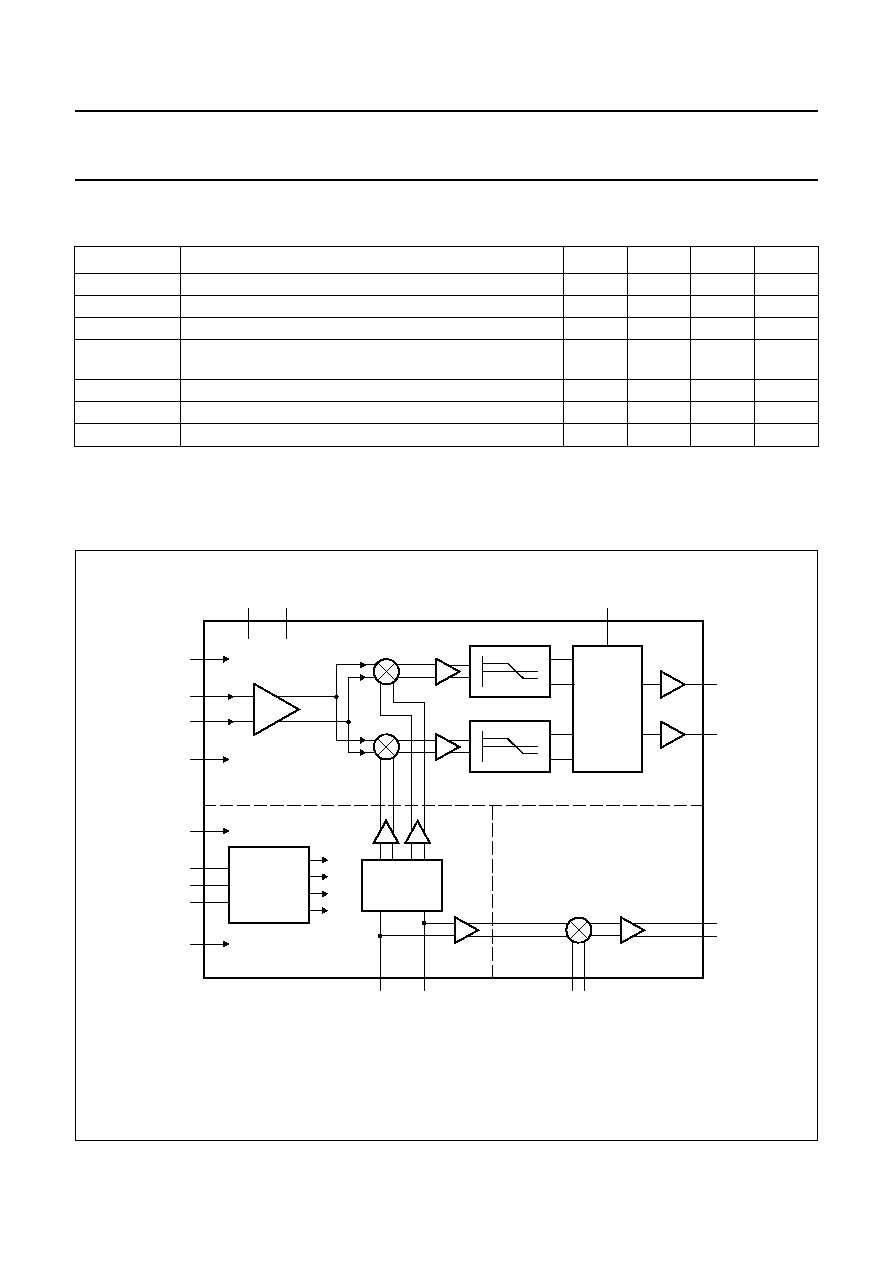
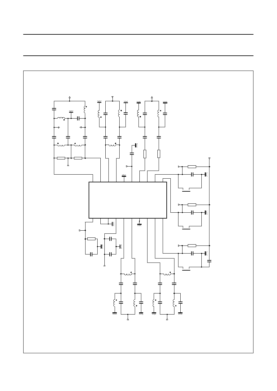
Image rejection is achieved in the internal architecture by
two RF mixers in quadrature and two all-pass filters in
I and Q IF channels that phase shift the IF by 45
∞
and 135
∞
respectively. The two phase shifted IFs are recombined
and buffered to furnish the IF output signal.
This means that signals presented at the RF input at
LO
-
IF frequency are rejected through this signal
processing while signals at LO + IF frequency can form the
IF signal.
The receiver section consists of a low-noise amplifier that
drives a quadrature mixer pair. The IF amplifier has
on-chip 45
∞
and 135
∞
phase shifting and a combining
network for image rejection.The IF driver has differential
open-collector type outputs.
The LO part consists of an internal all-pass type phase
shifter to provide quadrature LO signals to the receive
mixers. The all-pass filters outputs are buffered before
being fed to the receive mixers.
The transmit section consists of a down-conversion mixer
and a transmit IF driver stage. In the transmit mode an
internal LO buffer is used to drive the transmit IF
down-conversion mixer.
All RF and IF inputs or outputs are balanced to reduce
EMC issues.
Fast power-up switching is possible. A synthesizer-on
(SX) mode enables LO buffers independent of the other
circuits. When SXON pin is HIGH, all internal buffers on
the LO path of the circuit are turned on, thus minimizing
LO pulling when remainder of receive chain is
powered-up.
ORDERING INFORMATION
TYPE
NUMBER
PACKAGE
NAME
DESCRIPTION
VERSION
UAA2073AM
SSOP20
plastic shrink small outline package; 20 leads; body width 4.4 mm
SOT266-1
1997 Jan 27
3
Philips Semiconductors
Product specification
Image rejecting front-end
for GSM applications
UAA2073AM
QUICK REFERENCE DATA
Note 1.
Note
1. For conditions see Chapters "DC characteristics" and "AC characteristics".
BLOCK DIAGRAM
SYMBOL
PARAMETER
MIN.
TYP.
MAX.
UNIT
V
CC
supply voltage
3.6
3.75
5.3
V
I
CC(RX)
receive supply current
21
26
32
mA
I
CC(TX)
transmit supply current
9
12
15
mA
NF
RX
noise figure on demonstration board (including matching
and PCB losses)
-
3.6
4.7
dB
G
CPRX
conversion power gain
19
22
25
dB
IR
image frequency rejection
30
45
-
dB
T
amb
operating ambient temperature
-
30
+25
+75
∞
C
Fig.1 Block diagram.
handbook, full pagewidth
MGD149
LNA
IF
COMBINER
low-noise
amplifier
5
4
+
45
o
C
+
135
o
C
15
16
6
11
12
10
19
14
13
20
1
8
17
18
RX
TX
IF
LO
9
TXINA
TXINB
LOINB
MIXER
LOINA
2
3
IFA
IFB
TXOIFA
TXOIFB
n.c.
n.c.
SBS
QUADRATURE
PHASE
SHIFTER
CURRENT
REGULATORS
RFINA
RFINB
7
GND1
RXON
TXON
SXON
GND2
VCC1
VCC2
UAA2073AM
RECEIVE SECTION
TRANSMIT SECTION
LOCAL OSCILLATOR
SECTION
1997 Jan 27
4
Philips Semiconductors
Product specification
Image rejecting front-end
for GSM applications
UAA2073AM
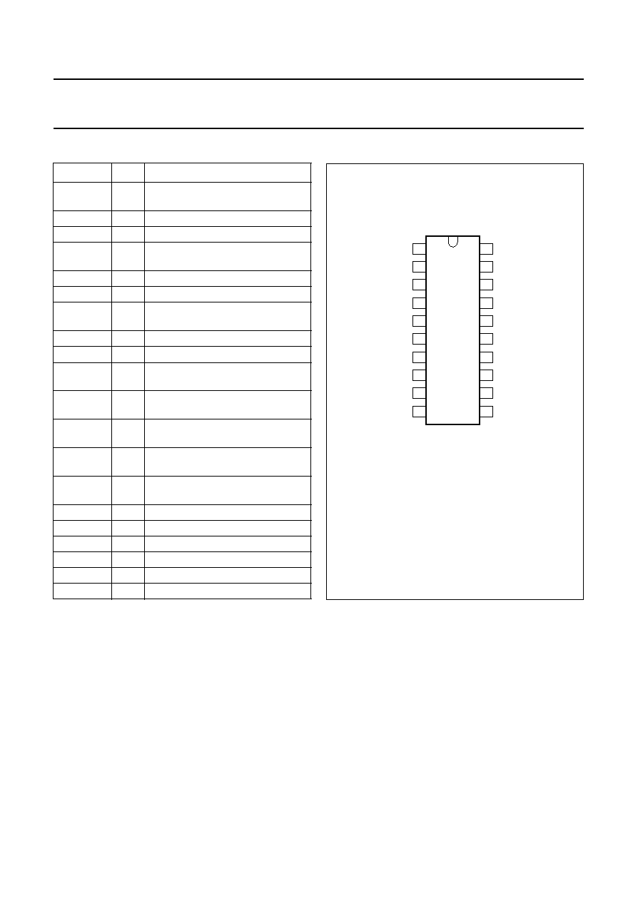
PINNING
SYMBOL
PIN
DESCRIPTION
SBS
1
sideband selection (should be
grounded for f
LO
< f
RF
)
n.c.
2
not connected
n.c.
3
not connected
V
CC1
4
supply voltage for receive and
transmit sections
RFINA
5
RF input A (balanced)
RFINB
6
RF input B (balanced)
GND1
7
ground 1 for receive and transmit
sections
TXINA
8
transmit mixer input A (balanced)
TXINB
9
transmit mixer input B (balanced)
SXON
10
hardware power-on of LO section
(including buffers to RX and TX)
RXON
11
hardware power-on for receive
section and LO buffers to RX
TXON
12
hardware power-on for transmit
section and LO buffers to TX
TXOIFB
13
transmit mixer IF output B
(balanced)
TXOIFA
14
transmit mixer IF output A
(balanced)
V
CC2
15
supply voltage for LO section
GND2
16
ground 2 for LO section
LOINB
17
LO input B (balanced)
LOINA
18
LO input A (balanced)
IFB
19
IF output B (balanced)
IFA
20
IF output A (balanced)
Fig.2 Pin configuration.
handbook, halfpage
UAA2073AM
MGD150
1
2
3
4
5
6
7
8
9
10
20
19
18
17
16
15
14
13
12
11
SBS
n.c.
n.c.
RFINA
RFINB
GND1
TXINA
TXINB
SXON
RXON
TXON
TXOIFB
TXOIFA
GND2
LOINB
LOINA
IFB
IFA
VCC1
VCC2
1997 Jan 27
5
Philips Semiconductors
Product specification
Image rejecting front-end
for GSM applications
UAA2073AM
FUNCTIONAL DESCRIPTION
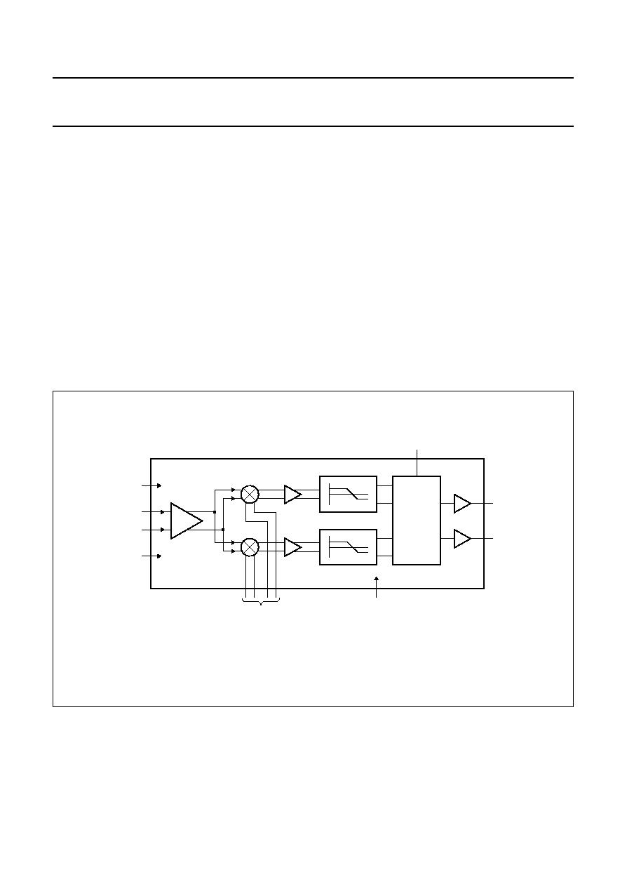
Receive section
The circuit contains a low-noise amplifier followed by two
high dynamic range mixers. These mixers are of the
Gilbert-cell type. The whole internal architecture is fully
differential.
The local oscillator, shifted in phase to 45
∞
and 135
∞
,
mixes the amplified RF to create I and Q channels.
The two I and Q channels are buffered, phase shifted by
45
∞
and 135
∞
respectively, amplified and recombined
internally to realize the image rejection.
Pin SBS allows sideband selection:
∑
f
LO
> f
RF
(SBS = 1)
∑
f
LO
< f
RF
(SBS = 0).
Where f
RF
is the frequency of the wanted signal.
Balanced signal interfaces are used for minimizing
crosstalk due to package parasitics. The RF differential
input impedance is 150
(parallel real part), chosen to
minimize current consumption at best noise performance.
The IF output is differential and of the open-collector type,
tuned for 175 MHz. Typical application will load the output
with a 680
resistor load at each IF output, plus a 1 k
load consisting in the input impedance of the IF filter or in
the input impedance of the matching network for the IF
filter. The power gain refers to the available power on this
1 k
load. The path to V
CC
for the DC current should be
achieved via tuning inductors. The output voltage is limited
to V
CC
+ 3V
be
or 3 diode forward voltage drops.
Fast switching, on/off, of the receive section is controlled
by the hardware input RXON.
Fig.3 Block diagram, receive section.
handbook, full pagewidth
MBH188
LNA
IF
COMBINER
IF
amplifier
IF
amplifier
MIXER
MIXER
RXON
LOIN
IFA
IFB
SBS
RFINA
RFINB
GND1
VCC1
+
45
o
+
135
o

1997 Jan 27
6
Philips Semiconductors
Product specification
Image rejecting front-end
for GSM applications
UAA2073AM
Local oscillator section
The Local Oscillator (LO) input directly drives the two
internal all-pass networks to provide quadrature LO to the
receive mixers.
The LO differential input impedance is 50
(parallel real
part).
A synthesizer-on (SX) mode is used to power-up the
buffering on the LO inputs, minimizing the pulling effect on
the external VCO when entering transmit or receive
modes.
This mode is active when the SXON input is HIGH. Table 1
shows status of circuit in accordance with TXON, RXON
and SXON inputs.
Transmit mixer
This mixer is used for down-conversion to the transmit IF.
Its inputs are coupled to the transmit RF and down-convert
it to a modulated transmit IF frequency which is phase
locked with the baseband modulation.
The transmit mixer provides a differential input at 200
and a differential output driver buffer for a 1 k
load.
The IF outputs are low impedance (emitter followers).
Fast switching, on/off, of the transmit section is controlled
by the hardware input TXON.
Fig.4 Block diagram, LO section.
handbook, halfpage
MBH189
LOINB
to TX
to RX
LOINA
QUAD
RXON
TXON
SXON
GND2
VCC2
Fig.5 Block diagram, transmit mixer.
handbook, halfpage
MBH190
TXINA
TXINB
TXON
LOIN
TX MIXER
TXOIFA
TXOIFB
1997 Jan 27
7
Philips Semiconductors
Product specification
Image rejecting front-end
for GSM applications
UAA2073AM
Table 1 Control of power status
LIMITING VALUES
In accordance with the Absolute Maximum Rating System (IEC 134).
HANDLING
Every pin withstands the ESD test in accordance with MIL-STD-883C class 2 (method 3015.5).
THERMAL CHARACTERISTICS
EXTERNAL PIN LEVEL
CIRCUIT MODE OF OPERATION
TXON
RXON
SXON
LOW
LOW
LOW
power-down mode
LOW
HIGH
LOW
RX mode: receive section and LO buffers to RX on
HIGH
LOW
LOW
TX mode: transmit section and LO buffers to TX on
LOW
LOW
HIGH
SX mode: complete LO section on
LOW
HIGH
HIGH
SRX mode: receive section on and SX mode active
HIGH
LOW
HIGH
STX mode: transmit section on and SX mode active
HIGH
HIGH
LOW
receive and transmit sections on; specification not guaranteed
HIGH
HIGH
HIGH
receive and transmit sections on; specification not guaranteed
SYMBOL
PARAMETER
MIN.
MAX.
UNIT
V
CC
supply voltage
-
9
V
GND
difference in ground supply voltage applied between GND1 and GND2
-
0.6
V
P
i(max)
maximum power input
-
+20
dBm
T
j(max)
maximum operating junction temperature
-
+150
∞
C
P
dis(max)
maximum power dissipation in stagnant air
-
250
mW
T
stg
IC storage temperature
-
65
+150
∞
C
SYMBOL
PARAMETER
VALUE
UNIT
R
th j-a
thermal resistance from junction to ambient in free air
120
K/W
1997 Jan 27
8
Philips Semiconductors
Product specification
Image rejecting front-end
for GSM applications
UAA2073AM
DC CHARACTERISTICS
V
CC
= 3.75 V; T
amb
= 25
∞
C; unless otherwise specified.
Note
1. The referenced inputs should be connected to a valid CMOS input level.
SYMBOL
PARAMETER
CONDITIONS
MIN.
TYP.
MAX.
UNIT
Pins: V
CC1
and V
CC2
V
CC
supply voltage
over full temperature range
3.6
3.75
5.3
V
I
CC(RX)
supply current in RX mode
21
26
32
mA
I
CC(TX)
supply current in TX mode
9
12
15
mA
I
CC(SX)
supply current in SX mode
4.5
5.8
7.0
mA
I
CC(SRX)
supply current in SRX mode
23
28
34
mA
I
CC(STX)
supply current in STX mode
12.5
15.0
19.5
mA
I
CC(PD)
supply current in power-down mode
-
0.01
50
µ
A
Pins: SXON, RXON, TXON and SBS
V
th
CMOS threshold voltage
note 1
-
1.25
-
V
V
IH
HIGH level input voltage
0.7V
CC
-
V
CC
V
V
IL
LOW level input voltage
-
0.3
-
0.8
V
I
IH
HIGH level static input current
pin at V
CC
-
0.4 V
-
1
-
+1
µ
A
I
IL
LOW level static input current
pin at 0.4 V
-
1
-
+1
µ
A
Pins: RFINA and RFINB
V
I(RFIN)
DC input voltage level
receive section on
2.0
2.2
2.4
V
Pins: IFA and IFB
I
O(IF)
DC output current
receive section on
2.3
3.0
3.8
mA
Pins: TXINA and TXINB
V
I(TXIN)
DC input voltage level
transmit section on
2.1
2.4
2.6
V
Pins: TXOIFA and TXOIFB
V
O(TXOIF)
DC output voltage level
transmit section on
1.8
1.9
2.1
V
Pins: LOINA and LOINB
V
I(LOIN)
DC input voltage level
receive section on
2.3
2.5
2.8
V
transmit section on
2.3
2.5
2.8
V
1997 Jan 27
9
Philips Semiconductors
Product specification
Image rejecting front-end
for GSM applications
UAA2073AM
AC CHARACTERISTICS
V
CC
= 3.75 V; T
amb
=
-
30 to +75
∞
C; f
IF
= 175 MHz; unless otherwise specified.
SYMBOL
PARAMETER
CONDITIONS
MIN.
TYP.
MAX.
UNIT
Receive section (receive section on)
R
iRX
RF input resistance (real part of
the parallel input impedance)
balanced; at 942.5 MHz
-
150
-
C
iRX
RF input capacitance (imaginary
part of the parallel input
impedance)
balanced; at 942.5 MHz
-
1
-
pF
f
iRX
RF input frequency
925
-
960
MHz
RL
iRX
return loss on matched RF input
note 1
15
20
-
dB
G
CPRX
conversion power gain
differential RF input to
differential IF output matched to
1 k
differential
19
22
25
dB
G
rip
gain ripple as a function of RF
frequency
note 2
-
0.2
0.5
dB
G/T
gain variation with temperature
note 2
-
20
-
15
-
10
mdB/K
DES1
1 dB desensitization input power
interferer frequency offset
3 MHz
-
-
30
-
dBm
CP1
RX
1 dB input compression point
note 1
-
25
-
23.0
-
dBm
IP2D
RX
half IF spurious rejection
(f
RF
= f
LO
+ 0.5f
IF
)
note 2
60
-
-
dB
IP3
RX
3rd order intercept point
referenced to the RF input
note 2
-
21.5
-
15
-
dBm
NF
RX
overall noise figure
RF input to differential IF output;
note 3
T
amb
= +25
∞
C
-
3.6
4.0
dB
over full temperature range
-
-
4.7
dB
R
LRX
typical application IF output load
impedance
balanced
-
1000
-
C
LRX
IF output load capacitance
unbalanced
-
-
2
pF
f
oRX
IF frequency range
-
175
-
MHz
IR
image frequency rejection
f
LO
< f
RF
30
45
-
dB
1997 Jan 27
10
Philips Semiconductors
Product specification
Image rejecting front-end
for GSM applications
UAA2073AM
Notes
1. Measured and guaranteed only on Philips UAA2073AM demonstration board at T
amb
= 25
∞
C.
2. Measured and guaranteed only on Philips UAA2073AM demonstration board.
3. This value includes printed-circuit board and balun losses on Philips UAA2073AM demonstration board over full
temperature range.
Local oscillator section (RXON or TXON or SXON = 1)
f
iLO
LO input frequency
750
-
785
MHz
R
iLO
LO input resistance (real part of
the parallel input impedance)
balanced; at 767.5 MHz
-
80
-
C
iLO
LO input capacitance (imaginary
part of the parallel input
impedance)
balanced; at 767.5 MHz
-
2
-
pF
RL
iLO
return loss on matched input
(including power-down mode)
note 2
10
15
-
dB
RL
iLO
return loss variation between SX,
SRX and STX modes
linear S
11
variation; note 1
-
20
-
mU
P
iLO
LO input power level
-
7
-
4
0
dBm
RI
LO
reverse isolation
LOIN to RFIN at LO frequency;
note 2
40
-
-
dB
Transmit section (transmit section on)
Z
oTX
TX IF output impedance
-
-
200
Z
LTX
TX IF load impedance
-
1
-
k
C
LTX
TX IF load capacitance
-
-
2
pF
R
iTX
TX RF input resistance
(real part of the parallel input
impedance)
balanced; at 897.5 MHz
-
200
-
C
iTX
TX RF input capacitance
(imaginary part of the parallel
input impedance)
balanced; at 897.5 MHz
-
1
-
pF
f
iTX
TX input frequency
880
-
915
MHz
RL
iTX
return loss on matched TX input
note 1
15
20
-
dB
G
CPTX
conversion power gain
from 200
to 1 k
output;
note 2
5
7.4
10
dB
f
oTX
TX output frequency
40
-
200
MHz
CP1
TX
1 dB input compression point
note 1
-
22
-
17.5
-
dBm
IP2
TX
2nd order intercept point
-
+20
-
dBm
IP3
TX
3rd order intercept point
-
12
-
9
-
dBm
NF
TX
noise figure
double sideband; notes 2 and 3
-
9.8
12
dB
RI
TX
reverse isolation
TXIN to LOIN; note 2
40
-
-
dB
I
TX
isolation
LOIN to TXIN; note 2
40
-
-
dB
Timing
t
start
start-up time of each block
1
5
20
µ
s
SYMBOL
PARAMETER
CONDITIONS
MIN.
TYP.
MAX.
UNIT
1997 Jan 27
11
Philips Semiconductors
Product specification
Image rejecting front-end
for GSM applications
UAA2073AM
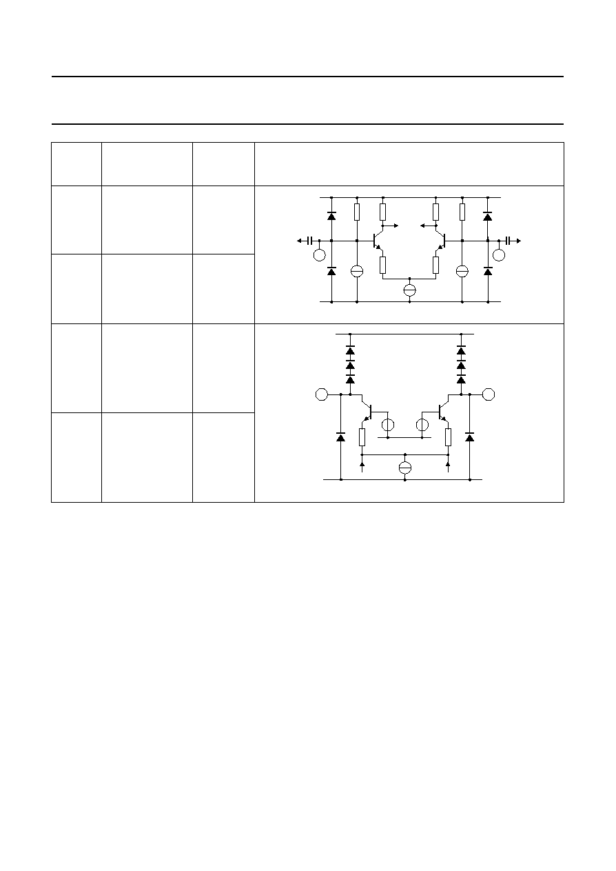
INTERNAL PIN CONFIGURATION
PIN
SYMBOL
DC
VOLTAGE
(V)
EQUIVALENT CIRCUIT
1
SBS
10
SXON
11
RXON
12
TXON
4
V
CC1
+3.75
15
V
CC2
+3.75
7
GND1
0
16
GND2
0
5
RFINA
+2.2
6
RFINB
+2.2
8
TXINA
+2.4
9
TXINB
+2.4
13
TXOIFB
+1.9
14
TXOIFA
+1.9
MBH682
VCC
GND
1
MBH683
VCC
GND
6, 9
5, 8
MBH684
VCC
GND
13, 14
1997 Jan 27
12
Philips Semiconductors
Product specification
Image rejecting front-end
for GSM applications
UAA2073AM
17
LOINB
+2.5
18
LOINA
+2.5
19
IFB
+3.0
20
IFA
+3.0
PIN
SYMBOL
DC
VOLTAGE
(V)
EQUIVALENT CIRCUIT
MBH685
VCC
GND
17
18
MBH686
19
20
VCC
GND
GND
1997 Jan 27
13
Philips Semiconductors
Product specification
Image rejecting front-end
for GSM applications
UAA2073AM
APPLICATION INFORMATION
Fig.6
Philips demonstration board diagram.
handbook, full pagewidth
MGD151
R3
680
R4
680
L11
120
nH
L12
120
nH
L9
22
nH
C17
3.9 pF
3.9 pF
220 pF
27 pF
27 pF
390 pF
390 pF
C19
C18
L16
100
nH
L15 100 nH
C34
8.2 pF
C33 8.2 pF
IFO
175 MHz
UAA2073AM
20
1
19
2
18
3
17
4
16
5
15
6
14
7
13
8
12
9
11
10
C27
27
pF
2
1
R10
680
k
TXON
C25
27
pF
2
1
R8
680
k
RXON
C26
27
pF
2
1
R9
680
k
SXON
L4
15 nH
C6
1.8 pF
C5
1.8 pF
L5
15 nH
C8
27 pF
C7
C28
27 pF
120 pF
L6
27 nH
C24
1 nF
C23
27 pF
R5
SBS
680 k
C20
27 pF
V
CC
V
CC
V
CC
V
CC
L3
15 nH
C1
1.5 pF
C3
1.5 pF
RFIN
925 to 960 MHz
TXIN
880 to 915 MHz
L2
15 nH
C2
27 pF
C4
27 pF
L1
18 nH
L7 12 nH
C10 3.3 pF
C9 3.3 pF
LOIN
750 to
785 MHz
L8 12 nH
C12
C11
27 pF
L13 180 nH
C32 6.8 pF
C31 6.8 pF
TXOIF
40 to
200 MHz
L14 180 nH
C13
C15
C14
IFB
IFA
R1
R2
180
180
1997 Jan 27
14
Philips Semiconductors
Product specification
Image rejecting front-end
for GSM applications
UAA2073AM
Table 2 UAA2073AM demonstration board parts list
PART
VALUE
SIZE
LOCATION
Resistors
R1
180
0805
TXOIF
R2
180
0805
TXOIF
R3
680
0805
IFO
R4
680
0805
IFO
R5
680 k
0805
SBS
R8
680 k
0805
RXON
R9
680 k
0805
SXON
R10
680 k
0805
TXON
Capacitors
C1
1.5 pF
0805
RFIN
C2
27 pF
0805
RFIN
C3
1.5 pF
0805
RFIN
C4
27 pF
0805
RFIN
C5
1.8 pF
0805
TXIN
C6
1.8 pF
0805
TXIN
C7
27 pF
0805
TXIN
C8
27 pF
0805
TXIN
C9
3.3 pF
0805
LOIN
C10
3.3 pF
0805
LOIN
C11
27 pF
0805
LOIN
C12
27 pF
0805
LOIN
C13
390 pF
0805
TXOIF
C14
390 pF
0805
TXOIF
C15
27 pF
0805
V
CCLO
C17
3.9 pF
0805
IFO
C18
3.9 pF
0805
IFO
C19
220 pF
0805
IF/V
CC
C20
27 pF
0805
SBS
C23
27 pF
0805
V
CCLNA
C24
1 nF
0805
V
CCLNA
C25
27 pF
0805
RXON
C26
27 pF
0805
SXON
C27
27 pF
0805
TXON
C28
120 pF
0805
V
CC
C31
6.8 pF
0805
TXOIF
C32
6.8 pF
0805
TXOIF
C33
8.2 pF
0805
IFO
C34
8.2 pF
0805
IFO
Other components
Component manufacturers
All surface mounted resistors and capacitors are from
Philips Components. The small value capacitors are
multilayer ceramic with NPO dielectric. The inductors are
from Coilcraft UK.
Inductors
L1
18 nH
0805
RFIN
L2
15 nH
0805
RFIN
L3
15 nH
0805
RFIN
L4
15 nH
0805
TXIN
L5
15 nH
0805
TXIN
L6
27 nH
0805
TXIN
L7
12 nH
0805
LOIN
L8
12 nH
0805
LOIN
L9
22 nH
0805
LOIN
L11
120 nH
1008
IFO
L12
120 nH
1008
IFO
L13
180 nH
0805
TXOIF
L14
180 nH
0805
TXOIF
L15
100 nH
1008
IFO
L16
100 nH
1008
IFO
COMPONENT
DESCRIPTIONS
IC1
UAA2073AM
SMA/RIM
sockets for RF and IF inputs/outputs
SMB
V
CC
socket
PART
VALUE
SIZE
LOCATION

1997 Jan 27
15
Philips Semiconductors
Product specification
Image rejecting front-end
for GSM applications
UAA2073AM
PACKAGE OUTLINE
UNIT
A
1
A
2
A
3
b
p
c
D
(1)
E
(1)
(1)
e
H
E
L
L
p
Q
Z
y
w
v
REFERENCES
OUTLINE
VERSION
EUROPEAN
PROJECTION
ISSUE DATE
IEC
JEDEC
EIAJ
mm
0.15
0
1.4
1.2
0.32
0.20
0.20
0.13
6.6
6.4
4.5
4.3
0.65
1.0
0.2
6.6
6.2
0.65
0.45
0.48
0.18
10
0
o
o
0.13
0.1
DIMENSIONS (mm are the original dimensions)
Note
1. Plastic or metal protrusions of 0.20 mm maximum per side are not included.
0.75
0.45
SOT266-1
90-04-05
95-02-25
w
M
A
A
1
A
2
b
p
D
H
E
L
p
Q
detail X
E
Z
e
c
L
v
M
A
X
(A )
3
A
y
0.25
1
10
20
11
pin 1 index
0
2.5
5 mm
scale
SSOP20: plastic shrink small outline package; 20 leads; body width 4.4 mm
SOT266-1
A
max.
1.5

1997 Jan 27
16
Philips Semiconductors
Product specification
Image rejecting front-end
for GSM applications
UAA2073AM
SOLDERING
Introduction
There is no soldering method that is ideal for all IC
packages. Wave soldering is often preferred when
through-hole and surface mounted components are mixed
on one printed-circuit board. However, wave soldering is
not always suitable for surface mounted ICs, or for
printed-circuits with high population densities. In these
situations reflow soldering is often used.
This text gives a very brief insight to a complex technology.
A more in-depth account of soldering ICs can be found in
our
"IC Package Databook" (order code 9398 652 90011).
Reflow soldering
Reflow soldering techniques are suitable for all SSOP
packages.
Reflow soldering requires solder paste (a suspension of
fine solder particles, flux and binding agent) to be applied
to the printed-circuit board by screen printing, stencilling or
pressure-syringe dispensing before package placement.
Several techniques exist for reflowing; for example,
thermal conduction by heated belt. Dwell times vary
between 50 and 300 seconds depending on heating
method. Typical reflow temperatures range from
215 to 250
∞
C.
Preheating is necessary to dry the paste and evaporate
the binding agent. Preheating duration: 45 minutes at
45
∞
C.
Wave soldering
Wave soldering is not recommended for SSOP packages.
This is because of the likelihood of solder bridging due to
closely-spaced leads and the possibility of incomplete
solder penetration in multi-lead devices.
If wave soldering cannot be avoided, the following
conditions must be observed:
∑
A double-wave (a turbulent wave with high upward
pressure followed by a smooth laminar wave)
soldering technique should be used.
∑
The longitudinal axis of the package footprint must
be parallel to the solder flow and must incorporate
solder thieves at the downstream end.
Even with these conditions, only consider wave
soldering SSOP packages that have a body width of
4.4 mm, that is SSOP16 (SOT369-1) or
SSOP20 (SOT266-1).
During placement and before soldering, the package must
be fixed with a droplet of adhesive. The adhesive can be
applied by screen printing, pin transfer or syringe
dispensing. The package can be soldered after the
adhesive is cured.
Maximum permissible solder temperature is 260
∞
C, and
maximum duration of package immersion in solder is
10 seconds, if cooled to less than 150
∞
C within
6 seconds. Typical dwell time is 4 seconds at 250
∞
C.
A mildly-activated flux will eliminate the need for removal
of corrosive residues in most applications.
Repairing soldered joints
Fix the component by first soldering two diagonally-
opposite end leads. Use only a low voltage soldering iron
(less than 24 V) applied to the flat part of the lead. Contact
time must be limited to 10 seconds at up to 300
∞
C. When
using a dedicated tool, all other leads can be soldered in
one operation within 2 to 5 seconds between
270 and 320
∞
C.

1997 Jan 27
17
Philips Semiconductors
Product specification
Image rejecting front-end
for GSM applications
UAA2073AM
DEFINITIONS
LIFE SUPPORT APPLICATIONS
These products are not designed for use in life support appliances, devices, or systems where malfunction of these
products can reasonably be expected to result in personal injury. Philips customers using or selling these products for
use in such applications do so at their own risk and agree to fully indemnify Philips for any damages resulting from such
improper use or sale.
Data sheet status
Objective specification
This data sheet contains target or goal specifications for product development.
Preliminary specification
This data sheet contains preliminary data; supplementary data may be published later.
Product specification
This data sheet contains final product specifications.
Limiting values
Limiting values given are in accordance with the Absolute Maximum Rating System (IEC 134). Stress above one or
more of the limiting values may cause permanent damage to the device. These are stress ratings only and operation
of the device at these or at any other conditions above those given in the Characteristics sections of the specification
is not implied. Exposure to limiting values for extended periods may affect device reliability.
Application information
Where application information is given, it is advisory and does not form part of the specification.

1997 Jan 27
18
Philips Semiconductors
Product specification
Image rejecting front-end
for GSM applications
UAA2073AM
NOTES

1997 Jan 27
19
Philips Semiconductors
Product specification
Image rejecting front-end
for GSM applications
UAA2073AM
NOTES

Internet: http://www.semiconductors.philips.com
Philips Semiconductors ≠ a worldwide company
© Philips Electronics N.V. 1997
SCA53
All rights are reserved. Reproduction in whole or in part is prohibited without the prior written consent of the copyright owner.
The information presented in this document does not form part of any quotation or contract, is believed to be accurate and reliable and may be changed
without notice. No liability will be accepted by the publisher for any consequence of its use. Publication thereof does not convey nor imply any license
under patent- or other industrial or intellectual property rights.
Netherlands: Postbus 90050, 5600 PB EINDHOVEN, Bldg. VB,
Tel. +31 40 27 82785, Fax. +31 40 27 88399
New Zealand: 2 Wagener Place, C.P.O. Box 1041, AUCKLAND,
Tel. +64 9 849 4160, Fax. +64 9 849 7811
Norway: Box 1, Manglerud 0612, OSLO,
Tel. +47 22 74 8000, Fax. +47 22 74 8341
Philippines: Philips Semiconductors Philippines Inc.,
106 Valero St. Salcedo Village, P.O. Box 2108 MCC, MAKATI,
Metro MANILA, Tel. +63 2 816 6380, Fax. +63 2 817 3474
Poland: Ul. Lukiska 10, PL 04-123 WARSZAWA,
Tel. +48 22 612 2831, Fax. +48 22 612 2327
Portugal: see Spain
Romania: see Italy
Russia: Philips Russia, Ul. Usatcheva 35A, 119048 MOSCOW,
Tel. +7 095 755 6918, Fax. +7 095 755 6919
Singapore: Lorong 1, Toa Payoh, SINGAPORE 1231,
Tel. +65 350 2538, Fax. +65 251 6500
Slovakia: see Austria
Slovenia: see Italy
South Africa: S.A. PHILIPS Pty Ltd., 195-215 Main Road Martindale,
2092 JOHANNESBURG, P.O. Box 7430 Johannesburg 2000,
Tel. +27 11 470 5911, Fax. +27 11 470 5494
South America: Rua do Rocio 220, 5th floor, Suite 51,
04552-903 S„o Paulo, S√O PAULO - SP, Brazil,
Tel. +55 11 821 2333, Fax. +55 11 829 1849
Spain: Balmes 22, 08007 BARCELONA,
Tel. +34 3 301 6312, Fax. +34 3 301 4107
Sweden: Kottbygatan 7, Akalla, S-16485 STOCKHOLM,
Tel. +46 8 632 2000, Fax. +46 8 632 2745
Switzerland: Allmendstrasse 140, CH-8027 ZÐRICH,
Tel. +41 1 488 2686, Fax. +41 1 481 7730
Taiwan: Philips Semiconductors, 6F, No. 96, Chien Kuo N. Rd., Sec. 1,
TAIPEI, Taiwan Tel. +886 2 2134 2870, Fax. +886 2 2134 2874
Thailand: PHILIPS ELECTRONICS (THAILAND) Ltd.,
209/2 Sanpavuth-Bangna Road Prakanong, BANGKOK 10260,
Tel. +66 2 745 4090, Fax. +66 2 398 0793
Turkey: Talatpasa Cad. No. 5, 80640 GÐLTEPE/ISTANBUL,
Tel. +90 212 279 2770, Fax. +90 212 282 6707
Ukraine: PHILIPS UKRAINE, 4 Patrice Lumumba str., Building B, Floor 7,
252042 KIEV, Tel. +380 44 264 2776, Fax. +380 44 268 0461
United Kingdom: Philips Semiconductors Ltd., 276 Bath Road, Hayes,
MIDDLESEX UB3 5BX, Tel. +44 181 730 5000, Fax. +44 181 754 8421
United States: 811 East Arques Avenue, SUNNYVALE, CA 94088-3409,
Tel. +1 800 234 7381
Uruguay: see South America
Vietnam: see Singapore
Yugoslavia: PHILIPS, Trg N. Pasica 5/v, 11000 BEOGRAD,
Tel. +381 11 625 344, Fax.+381 11 635 777
For all other countries apply to: Philips Semiconductors, Marketing & Sales Communications,
Building BE-p, P.O. Box 218, 5600 MD EINDHOVEN, The Netherlands, Fax. +31 40 27 24825
Argentina: see South America
Australia: 34 Waterloo Road, NORTH RYDE, NSW 2113,
Tel. +61 2 9805 4455, Fax. +61 2 9805 4466
Austria: Computerstr. 6, A-1101 WIEN, P.O. Box 213,
Tel. +43 1 60 101, Fax. +43 1 60 101 1210
Belarus: Hotel Minsk Business Center, Bld. 3, r. 1211, Volodarski Str. 6,
220050 MINSK, Tel. +375 172 200 733, Fax. +375 172 200 773
Belgium: see The Netherlands
Brazil: see South America
Bulgaria: Philips Bulgaria Ltd., Energoproject, 15th floor,
51 James Bourchier Blvd., 1407 SOFIA,
Tel. +359 2 689 211, Fax. +359 2 689 102
Canada: PHILIPS SEMICONDUCTORS/COMPONENTS,
Tel. +1 800 234 7381
China/Hong Kong: 501 Hong Kong Industrial Technology Centre,
72 Tat Chee Avenue, Kowloon Tong, HONG KONG,
Tel. +852 2319 7888, Fax. +852 2319 7700
Colombia: see South America
Czech Republic: see Austria
Denmark: Prags Boulevard 80, PB 1919, DK-2300 COPENHAGEN S,
Tel. +45 32 88 2636, Fax. +45 31 57 1949
Finland: Sinikalliontie 3, FIN-02630 ESPOO,
Tel. +358 9 615800, Fax. +358 9 61580/xxx
France: 4 Rue du Port-aux-Vins, BP317, 92156 SURESNES Cedex,
Tel. +33 1 40 99 6161, Fax. +33 1 40 99 6427
Germany: Hammerbrookstraþe 69, D-20097 HAMBURG,
Tel. +49 40 23 53 60, Fax. +49 40 23 536 300
Greece: No. 15, 25th March Street, GR 17778 TAVROS/ATHENS,
Tel. +30 1 4894 339/239, Fax. +30 1 4814 240
Hungary: see Austria
India: Philips INDIA Ltd, Shivsagar Estate, A Block, Dr. Annie Besant Rd.
Worli, MUMBAI 400 018, Tel. +91 22 4938 541, Fax. +91 22 4938 722
Indonesia: see Singapore
Ireland: Newstead, Clonskeagh, DUBLIN 14,
Tel. +353 1 7640 000, Fax. +353 1 7640 200
Israel: RAPAC Electronics, 7 Kehilat Saloniki St, TEL AVIV 61180,
Tel. +972 3 645 0444, Fax. +972 3 649 1007
Italy: PHILIPS SEMICONDUCTORS, Piazza IV Novembre 3,
20124 MILANO, Tel. +39 2 6752 2531, Fax. +39 2 6752 2557
Japan: Philips Bldg 13-37, Kohnan 2-chome, Minato-ku, TOKYO 108,
Tel. +81 3 3740 5130, Fax. +81 3 3740 5077
Korea: Philips House, 260-199 Itaewon-dong, Yongsan-ku, SEOUL,
Tel. +82 2 709 1412, Fax. +82 2 709 1415
Malaysia: No. 76 Jalan Universiti, 46200 PETALING JAYA, SELANGOR,
Tel. +60 3 750 5214, Fax. +60 3 757 4880
Mexico: 5900 Gateway East, Suite 200, EL PASO, TEXAS 79905,
Tel. +9-5 800 234 7381
Middle East: see Italy
Printed in The Netherlands
437027/1200/02/pp20
Date of release: 1997 Jan 27
Document order number:
9397 750 01642