 | –≠–ª–µ–∫—Ç—Ä–æ–Ω–Ω—ã–π –∫–æ–º–ø–æ–Ω–µ–Ω—Ç: UAA3522HL | –°–∫–∞—á–∞—Ç—å:  PDF PDF  ZIP ZIP |

DATA SHEET
Objective specification
File under Integrated Circuits, IC17
2000 Feb 18
INTEGRATED CIRCUITS
UAA3522HL
Low power dual-band GSM
transceiver with an image rejecting
front-end

2000 Feb 18
2
Philips Semiconductors
Objective specification
Low power dual-band GSM transceiver
with an image rejecting front-end
UAA3522HL
FEATURES
∑
Dual-band application for Global System for Mobile
communication (GSM) and Digital Cellular
communication Systems (DCS)
∑
Low noise and wide dynamic range single Intermediate
Frequency (IF) transceiver
∑
More than 30 dB on-chip image rejection in the receiver
∑
More than 60 dB gain control range
∑
I/Q demodulator with high performance integrated
baseband channel filter
∑
High precision I/Q modulator
∑
Transmit modulation loop architecture including offset
mixer and phase detector
∑
Dual Phase-Locked Loop (PLL) with on-chip IF Voltage
Controlled Oscillator (VCO)
∑
Fully differential design minimizing cross-talk and spurii
∑
3-wire serial bus interface
∑
Functional down to 2.7 V and up to 3.3 V
∑
LQFP48 package.
APPLICATIONS
∑
GSM 900 MHz hand-held transceiver
∑
GSM/DCS dual-band solution with the UAA2077CM
(down to 3.2 V) or UAA2077TS/D (down to 2.7 V).
GENERAL DESCRIPTION
The UAA3522HL integrates the receiver and most of the
transmitter section of a GSM hand-held transceiver. It also
integrates the receiver IF and the transmitter section of a
DCS transceiver.
The receiver comprises an RF and an IF section. The RF
(GSM) front-end amplifies the aerial signal, converts the
chosen channel frequency to an IF of 200 MHz, and also
provides more than 30 dB of image suppression. Some
selectivity is provided at this stage by an off-chip bandpass
pre-filter. The IF section further amplifies the chosen
channel, maintains the gain at the required level,
demodulates the signal into I and Q components, and
provides channel selectivity at a baseband stage using a
high performance integrated low-pass filter. The IF gain
can be varied over a range of more than 60 dB. The offset
at the I and Q outputs can be cancelled out by software
using the 3-wire serial programming bus.
The input Low Noise Amplifier (LNA) can be switched off
via the bus to allow accurate calibration in the offset
cancellation mode.
The transmitter comprises a high precision I/Q modulator
and modulation loop architecture. The I/Q modulator
converts the baseband modulation frequency to the
transmit IF. The modulation loop architecture, which
includes an on-chip offset mixer and phase detector,
controls an external transmit RF VCO which converts the
transmit modulated IF signal to RF.
A receive RF VCO provides the Local Oscillator (LO)
signal to the image rejection mixers in the RF receiver. An
IF VCO provides the LO signal to the I/Q demodulator and
I/Q modulator in the receiver and transmitter sections
respectively.
The frequencies of the RF VCO and the IF VCO are set by
internal PLL circuits, which are programmable via the
3-wire serial bus. The RF and IF PLL comparison
frequencies are 200 kHz and 1 MHz respectively, derived
from a 13 MHz reference signal which has to be supplied
externally. The quadrature RF LO signals required by the
image rejection mixers are obtained using on-chip
Resistor Capacitor (RC) networks. The quadrature IF LO
signals required by the I/Q modulator and I/Q demodulator
are obtained by dividing the frequency of the IF VCO
signal.
The IC can be powered on in either receiver (RX),
transmitter (TX) or synthesizer (SYN) operating mode
depending on the logic level at pins RXON, TXON and
SYNON, respectively. Alternatively, an operating mode
can be selected by software using the 3-wire serial
programming bus. In RX or TX mode, only those sections
of the IC which are required are switched on.
The GSM or DCS band is selected by the 3-wire serial
programming bus. When activating RX mode for DCS
applications, the receiver RF section can be disabled by
software so that only the receiver IF section is
powered-on.
The SYN mode is used to power-on the synthesizer prior
to activating the RX or TX mode. In SYN mode, some
internal LO buffers are also powered-on to minimize the
`pulling' effect of the VCO when either the receiver or the
transmitter are switched on.

2000 Feb 18
3
Philips Semiconductors
Objective specification
Low power dual-band GSM transceiver
with an image rejecting front-end
UAA3522HL
QUICK REFERENCE DATA
ORDERING INFORMATION
SYMBOL
PARAMETER
MIN.
TYP.
MAX.
UNIT
f
i(RF)(RX)
GSM band RF input frequency in RX mode
925
-
960
MHz
f
o(RF)(TX)(GSM)
GSM band RF output frequency in TX mode
880
-
915
MHz
f
o(RF)(TX)(DCS)
DCS band RF output frequency in TX mode
1710
-
1785
MHz
f
IF
IF frequency in all modes
-
200
-
MHz
TYPE
NUMBER
PACKAGE
NAME
DESCRIPTION
VERSION
UAA3522HL
LQFP48
plastic low profile quad flat package; 48 leads; body
7
◊
7
◊
1.4 mm
SOT313-2

2000
Feb
18
4
Philips Semiconductors
Objectiv
e specification
Lo
w po
w
er dual-band GSM tr
ansceiv
er
with an image rejecting front-end
U
AA3522HL
This text is here in white to force landscape pages to be rotated correctly when browsing through the pdf in the Acrobat reader.This text is here in
_
white to force landscape pages to be rotated correctly when browsing through the pdf in the Acrobat reader.This text is here inThis text is here in
white to force landscape pages to be rotated correctly when browsing through the pdf in the Acrobat reader. white to force landscape pages to be ...
BLOCK DIA
GRAM
h
andbook, full pagewidth
FCA004
UAA3522HL
UAA2077XM
90
∞
90
∞
0
∞
0
∞
DIVIDER &
PHASE
SHIFTER
IF VCO
XTAL
PROGRAMMABLE
DIVIDER
PROGRAMMABLE
DIVIDER
BALUN
DIVIDER
˜
13
DIVIDER
˜
5
˜
2
I
Q
I
Q
4, 5
2, 3
4, 5
2, 3
38, 39
44, 45
30, 31
8, 9
46, 47
IF PHASE/
FREQUENCY
DETECTOR
RF PHASE/
FREQUENCY
DETECTOR
CHARGE
PUMP
IF VCO
400 MHz
REF OSC.
13 MHz
23
16
13,
14
RX/TX
SWITCH
POWER
AMPLIFIER
GSM RF
RX VCO
1080 to 1160
MHz
GSM TX RF VCO
880 to 915 MHz
880 to 915 MHz
GSM BAND
925 to 960 MHz
DCS TX RF VCO
1710 to 1785 MHz
DCS RF
RX VCO
1510 to 1680
MHz
1710 to 1785 MHz
DCS BAND
1805 to1880 MHz
CHARGE
PUMP
35
26
41,
42
CHARGE
PUMP
PHASE
DETECTOR
PHASE
SHIFTER
PHASE
SHIFTER
◊
◊
◊
0
∞
90
∞
◊
◊
◊
◊
ADDER
+
ADDER
+
BALUN
PHASE
SHIFTER
PHASE
SHIFTER
0
∞
90
∞
90
∞
90
∞
◊
◊
ADDER
+
SAW
B
A
S
E
B
A
N
D
&
A
U
D
I
O
I
N
T
E
R
F
A
C
E
Fig.1 Block diagram.
2000 Feb 18
5
Philips Semiconductors
Objective specification
Low power dual-band GSM transceiver
with an image rejecting front-end
UAA3522HL
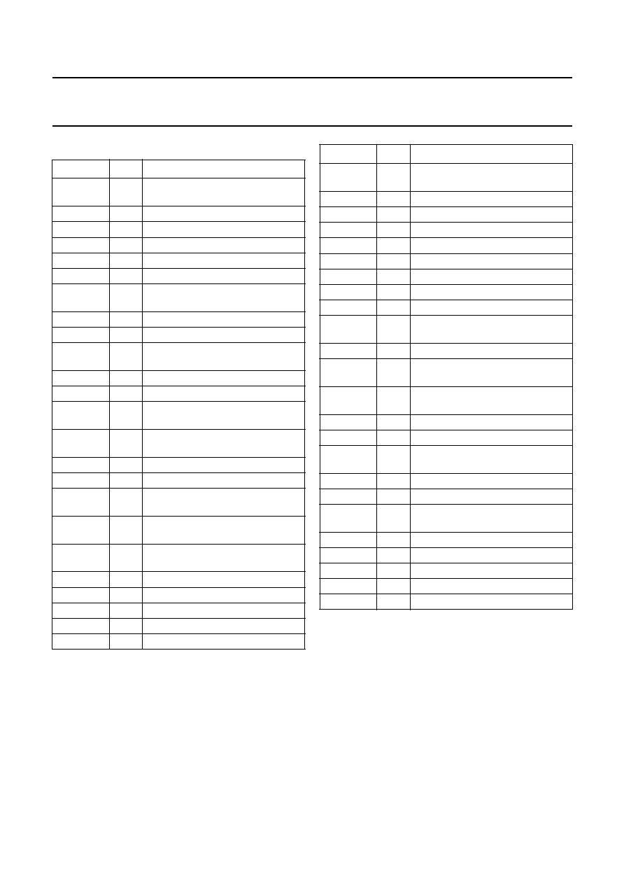
PINNING
SYMBOL
PIN
DESCRIPTION
V
CCIF1
1
IF section of RF receiver supply
voltage 1
QA
2
Q path A baseband input/output
QB
3
Q path B baseband input/output
IA
4
I path A baseband input/output
IB
5
I path B baseband input/output
REFAGC
6
AGC reference resistor
GNDIF2
7
I/Q modulator and I/Q demodulator
ground 2
RXIIFA
8
RX IF input A to AGC amplifier
RXIIFB
9
RX IF input B to AGC amplifier
V
CCIF2
10
I/Q modulator and I/Q demodulator
supply voltage 2
TXON
11
TX mode control pin
V
CCIFLO
12
IF LO supply voltage
IFLOC
13
IF LO signal input from
IF VCO resonator
IFLOE
14
IF LO signal input from
IF VCO resonator
GNDIFLO
15
IF LO ground
CPOIF
16
IF charge pump output
GNDCPIF
17
IF charge pump and phase
detector ground
V
CCCPIF
18
IF charge pump and phase
detector supply voltage
EN
19
serial programming bus enable
control pin
DATA
20
serial programming bus data input
CLK
21
serial programming bus clock input
GNDSYN
22
synthesizer ground
REFIN
23
13 MHz reference input
V
CCSYN
24
synthesizer supply voltage
V
CCCPRF
25
RF charge pump and phase
detector supply voltage
CPORF
26
RF charge pump output
GNDCP
27
RF charge pump ground
SYNON
28
SYN mode control pin
V
CCRFLO
29
RF LO section supply voltage
RFLOC
30
LO signal input from RF VCO
RFLOE
31
LO signal input from RF VCO
GNDRFLO
32
RF LO section ground
RXON
33
RX mode control pin
GNDPHD
34
transmit modulation loop charge
pump ground
PHDOUT
35
charge pump output
V
CCPHD
36
transmit modulation loop charge
pump supply voltage
RESEXT
37
reference resistor for transmit
modulation loop
TXIRFA
38
TX RF VCO signal input
TXIRFB
39
TX RF VCO signal input
V
CCRF
40
RF receiver and transmit
modulation loop supply voltage
RXIRFA
41
RF receiver input A
RXIRFB
42
RF receiver input B
GNDRF
43
RF receiver and transmit
modulation loop ground
TXIFA
44
transmit IF external filter A
TXIFB
45
transmit IF external filter B
RXOIFA
46
receiver IF output A
RXOIFB
47
receiver IF output B
GNDIF1
48
IF section of RF receiver ground 1
SYMBOL
PIN
DESCRIPTION