 | –≠–ª–µ–∫—Ç—Ä–æ–Ω–Ω—ã–π –∫–æ–º–ø–æ–Ω–µ–Ω—Ç: UBA1706 | –°–∫–∞—á–∞—Ç—å:  PDF PDF  ZIP ZIP |
DATA SHEET
Objective specification
Supersedes data of 1999 Mar 08
File under Integrated Circuits, IC17
1999 Jun 04
INTEGRATED CIRCUITS
UBA1706
Cordless telephone line interface

1999 Jun 04
2
Philips Semiconductors
Objective specification
Cordless telephone line interface
UBA1706
FEATURES
Line interface
∑
Low DC line voltage; operates down to 1.2 V (excluding
polarity guard)
∑
Voltage regulator with adjustable DC voltage
∑
DC mask for voltage or current regulation (CTR21)
∑
Line current limitation for protection
∑
Electronic hook switch control input
∑
Transmit amplifier with:
≠ Symmetrical inputs
≠ Fixed gain
≠ Large signal handling capability.
∑
Receive amplifier with fixed gain
∑
Transmit and receive amplifiers Automatic Gain Control
(AGC) for line loss compensation.
General purpose switches
Two switches with open-collector.
3-wire serial bus interface
Allows control of:
∑
DC mask (voltage or current regulation)
∑
Receive amplifier mute function
∑
AGC:
≠ On/off
≠ Slope
≠ I
start
line current.
∑
The state of the general purpose switches
∑
Global power-down mode.
Supply
Operates with external supply voltage from 3.0 to 5.5 V.
APPLICATIONS
∑
Cordless base stations
∑
Mains or battery-powered telephone sets.
GENERAL DESCRIPTION
The UBA1706 is a BiCMOS integrated circuit intended for
use in mains-powered telecom terminals. It performs all
speech and line interface functions, DC mask for voltage
or current regulation and electronic hook switch control.
The device also includes general purpose switches.
Most of the characteristics are programmable via a 3-wire
serial bus interface.
ORDERING INFORMATION
TYPE
NUMBER
PACKAGE
NAME
DESCRIPTION
VERSION
UBA1706TS
SSOP24
plastic shrink small outline package; 24 leads; body width 5.3 mm
SOT340-1

1999 Jun 04
3
Philips Semiconductors
Objective specification
Cordless telephone line interface
UBA1706
QUICK REFERENCE DATA
I
line
= 15 mA; V
CC
= 3.3 V; R
SLPE
= 10
; AGC pin connected to GND; Z
line
= 600
; Z
SET
= 619
; EHI = HIGH;
f = 1 kHz; T
amb
= 25
∞
C; bit AGC at logic 1, all other configuration bits at logic 0; measured in the test circuit of Fig.14;
unless otherwise specified.
SYMBOL
PARAMETER
CONDITIONS
MIN.
TYP.
MAX.
UNIT
V
CC
supply voltage
3.0
-
5.5
V
I
CC
current consumption from pin V
CC
normal operation; bit PD = 0
-
2.2
3.2
mA
power-down mode; bit PD = 1
-
110
150
µ
A
I
line
line current operating range
normal operation
11
-
140
mA
with reduced performance
3
-
11
mA
V
LN
DC line voltage
2.7
3.0
3.3
V
R
REGC
DC mask slope in current regulation
mode
I
line
> 35 mA (typical);
R
LVI
= 1 M
; R
RGL
= 7.15 k
;
bit CRC = 1
-
1.4
-
k
G
v(trx)
voltage gain
transmit amplifier from TXI to LN
V
TXI
= 50 mV (RMS)
10.6
11.6
12.6
dB
receive amplifier from RXI to RXO V
RXI
= 2 mV (RMS)
36.9
37.9
38.9
dB
G
v(trx)
gain control range for transmit and
receive amplifiers with respect to
I
line
= 15 mA
I
line
= 90 mA
-
6.5
-
dB

1999 Jun 04
4
Philips Semiconductors
Objective specification
Cordless telephone line interface
UBA1706
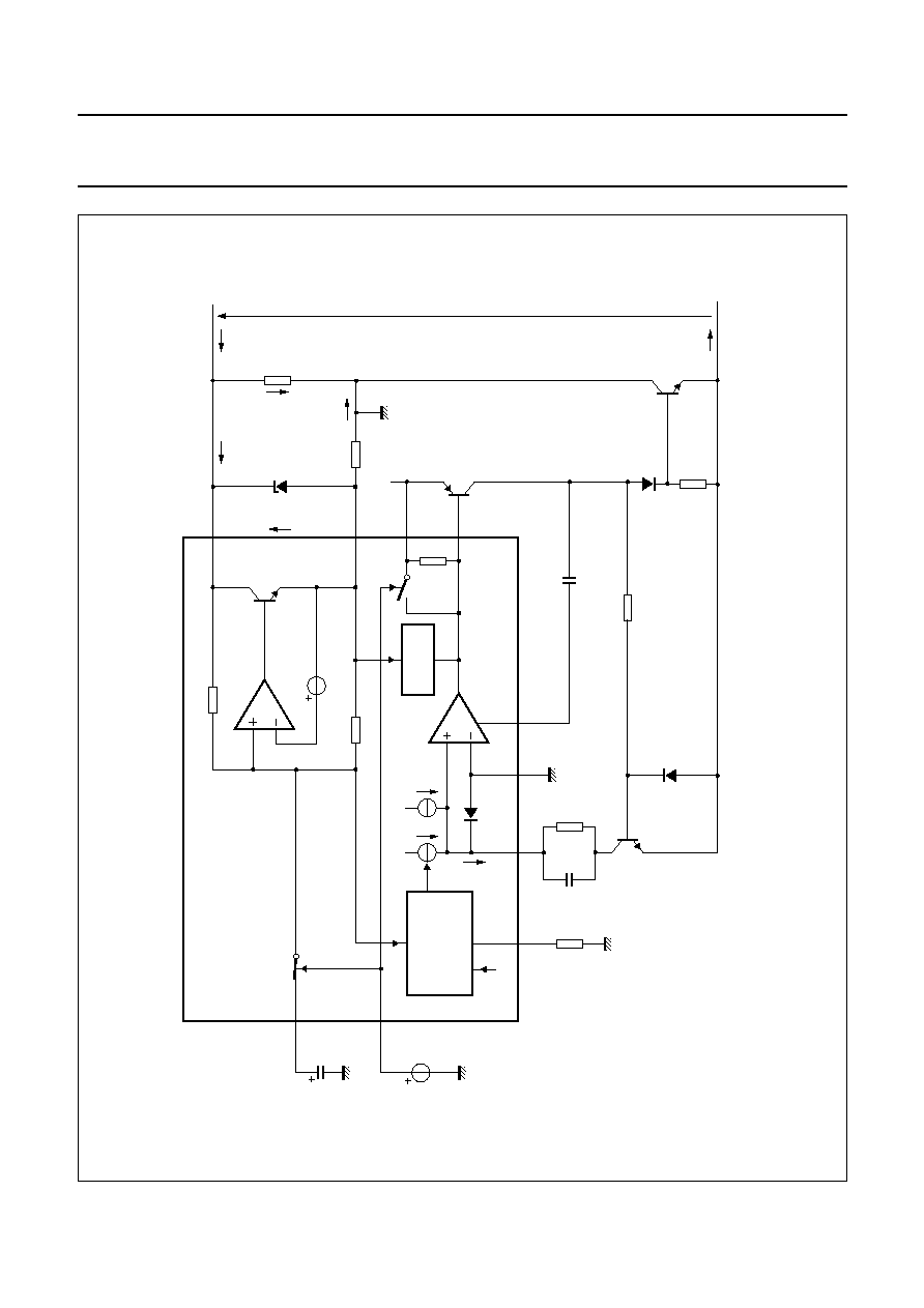
BLOCK DIAGRAM
Fig.1 Block diagram.
Bit names are given in italics.
handbook, full pagewidth
2
REG
SWITCH DRIVER
PROTECTION
2Vd
LVI
3
RGL
n.c.
4
16, 20, 22, 23
AGC
8
TXI
-
14
TXI
+
15
RXI
9
LINE INTERFACE
LINE
INTERFACE
UBA1706
CRC
RAGC1
SAGC,
AGC
RAGC2
RXM
EHI
EHI
RX PREAMP
TX PREAMP
EHI
600 mV
300 mV
AGC
CURRENT
LIMITATION
200 nA
VCC
CST
6
LCC
5
EHI
10
REG
2
SLPE
24
LN
1
RXO
7
GND
19
CCST
RLVI
VCC
TPDARL
D
TNSW
TNON-HOOK
SLPE
LOW VOLTAGE
PART
VCC 21
2Vd
RSLPE
ZSET
CREG
MBL039
SERIAL
INTERFACE
EN
CLK
DATA
12
13
11
9
SUPPLY
PD
GENERAL SWITCHES
SWI1
SWI2
18
17
SWC1, SWC2
2
RRGL
V
I
V
I
1999 Jun 04
5
Philips Semiconductors
Objective specification
Cordless telephone line interface
UBA1706
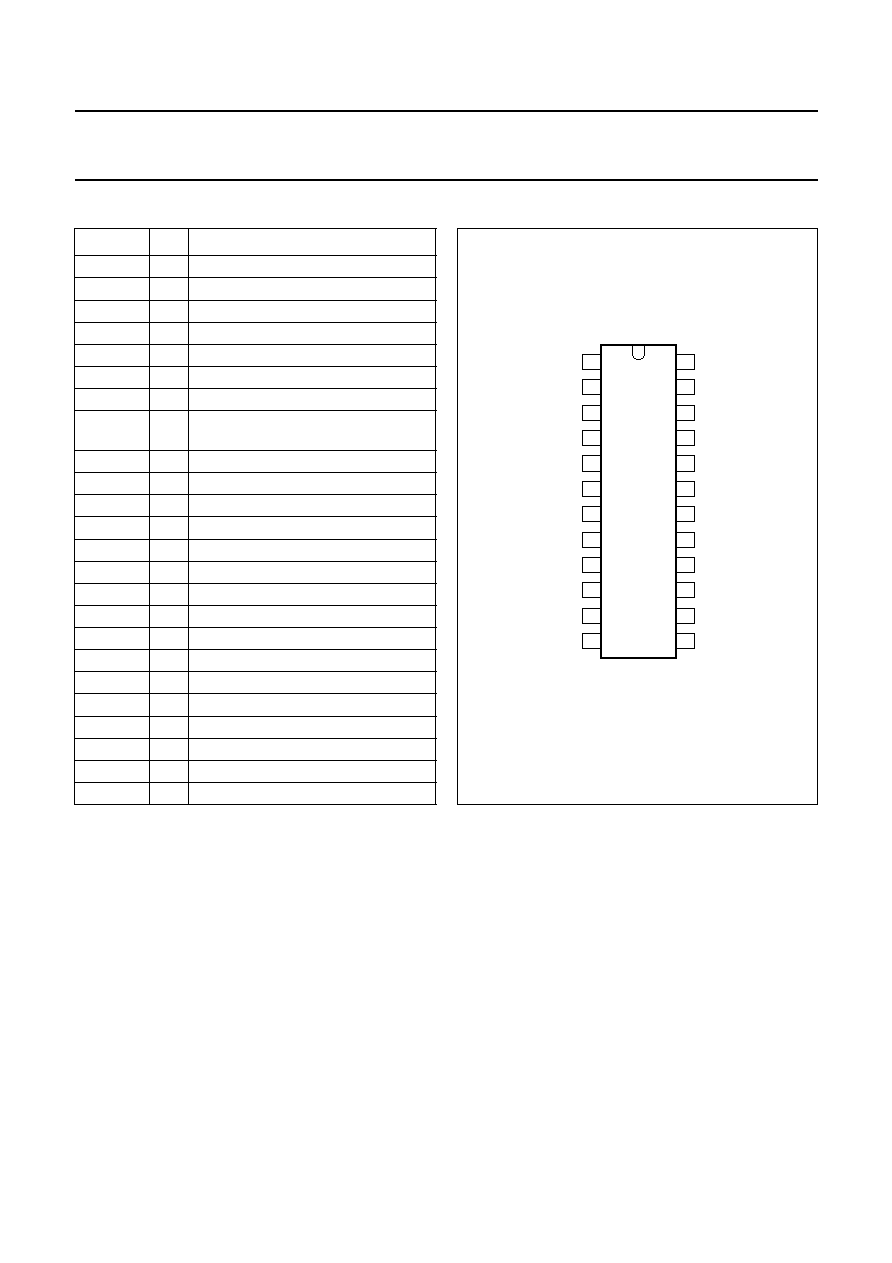
PINNING
SYMBOL
PIN
DESCRIPTION
LN
1
positive line terminal
REG
2
line voltage regulator decoupling
LVI
3
negative line voltage sense input
RGL
4
reference for current regulation mode
LCC
5
line current control output
CST
6
input for stability capacitor
RXO
7
receive amplifier output
AGC
8
automatic gain control/line loss
compensation adjustment
RXI
9
receiver amplifier input
EHI
10
electronic hook switch control input
DATA
11
serial bus data input
EN
12
programming serial bus enable input
CLK
13
serial bus clock input
TXI
-
14
inverted transmit amplifier input
TXI+
15
non-inverted transmit amplifier input
n.c.
16
not connected
SWI2
17
NPN open-collector output 2
SWI1
18
NPN open-collector output 1
GND
19
ground reference
n.c.
20
not connected
V
CC
21
supply voltage
n.c.
22
not connected
n.c.
23
not connected
SLPE
24
connection for slope resistor
Fig.2 Pin configuration.
handbook, halfpage
UBA1706
FCA031
1
2
3
4
5
6
7
8
9
10
11
12
LN
REG
LVI
RGL
LCC
CST
RXO
AGC
RXI
EHI
DATA
EN
SLPE
n.c.
n.c.
VCC
n.c.
GND
SW1
SW2
n.c.
TXI+
TXI-
CLK
24
23
22
21
20
19
18
17
16
15
14
13
1999 Jun 04
6
Philips Semiconductors
Objective specification
Cordless telephone line interface
UBA1706
FUNCTIONAL DESCRIPTION
All data given in this chapter consists of typical values,
except when otherwise specified.
Supply (pins V
CC
and GND; bit PD)
The UBA1706 must be supplied with an external stabilized
voltage source across pins V
CC
and GND.
Without any signal and without any general purpose switch
selected, the internal current consumption is 2.2 mA at
V
CC
= 3.3 V. Each selected switch (pins SWI1 or SWI2)
increases the current consumption by 600
µ
A.
To drastically reduce current consumption, the UBA1706
is provided with a power-down mode controlled by bit PD.
When bit PD is at logic 1, the current consumption from
V
CC
becomes 110
µ
A. In the power-down mode, the serial
interface is the only function which remains active.
Line interface
DC
CHARACTERISTICS
(
PINS
LN, SLPE, REG, CST, LVI,
LCC, RGL
AND
GND;
BIT
CRC)
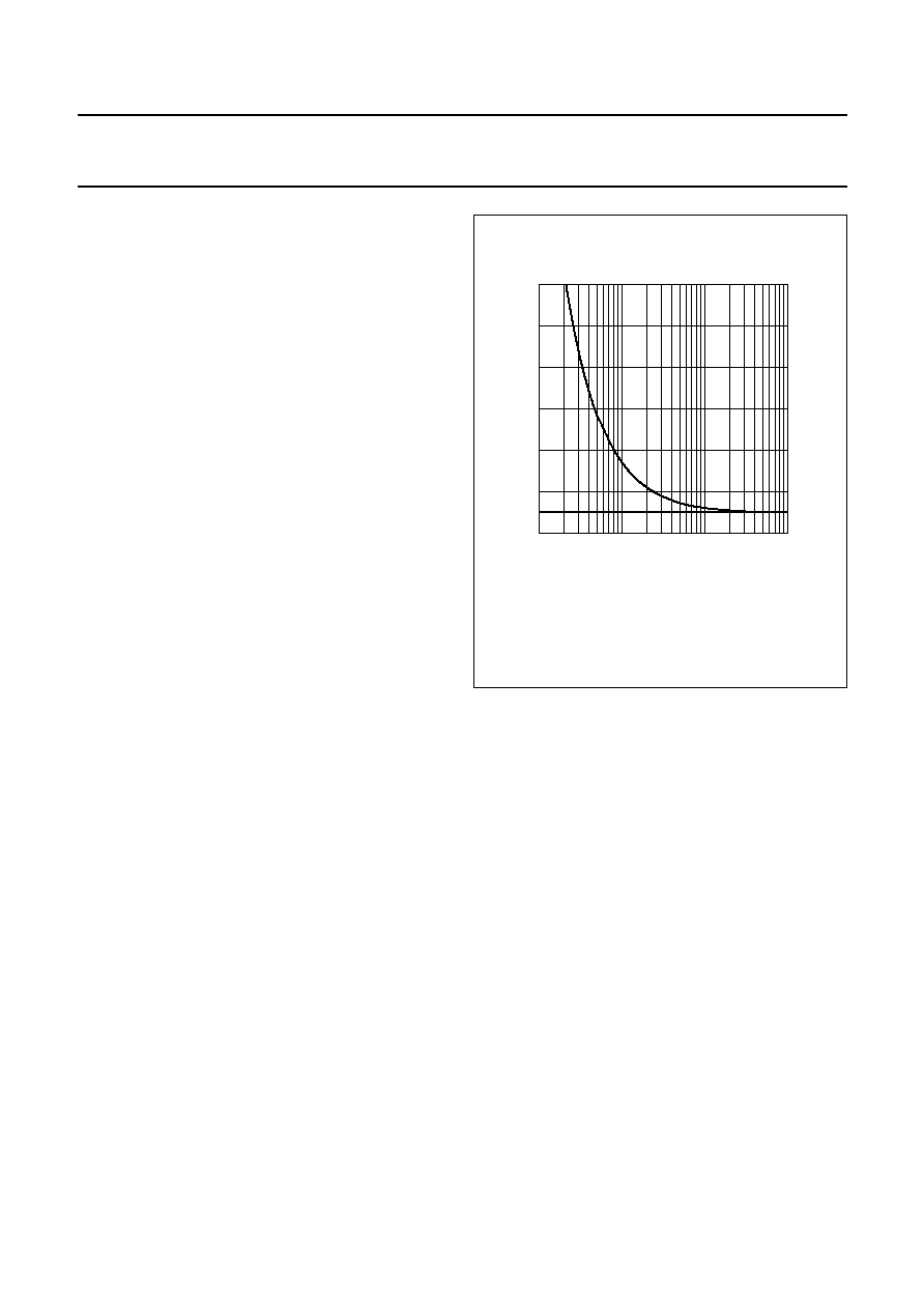
The IC generates a stabilized reference voltage (V
ref
)
across pins LN and SLPE. This reference voltage is equal
to 2.9 V, is temperature compensated and can be adjusted
by means of an external resistor (R
VA
). The reference
voltage can be increased by connecting the R
VA
resistor
between pins REG and SLPE (see Fig.3).
The voltage at pin REG is used by the internal regulator to
generate the stabilized reference voltage and is decoupled
by a capacitor (C
REG
) which is connected to GND. This
capacitor, converted to an equivalent inductance
(see Section "Set impedance") realizes the set impedance
conversion from its DC value (R
SLPE
) to its AC value
(Z
SET
in the audio frequency range). Figure 4 illustrates
the reference voltage supply configuration. As can be seen
from Fig.4, part of the line current flows into the Z
SET
impedance network and is not sensed by the UBA1706.
Therefore, using the R
VA
resistor to change the value of
the reference voltage will also modify all parameters
related to the line current such as:
∑
The AGC
∑
The DC mask management
∑
The low voltage area characteristics.
In the same way, changing the value of Z
SET
also affects
the characteristics. The IC has been optimized for
V
ref
= 2.9 V and Z
SET
= 619
.
The IC regulates the line voltage at pin LN, which can be
calculated as follows:
Where:
I
line
= line current
I
ZSET
= current flowing through Z
SET
I* = current consumed between LN and GND
(approximately 100
µ
A).
The preferred value for R
SLPE
is 10
. Changing R
SLPE
will
affect more than the DC characteristics; it also influences
the transmit gain, the gain control characteristics, the
sidetone level and the maximum output swing on the line.
Nevertheless, for compliance with CTR21, 8.66
is the
optimum value for R
SLPE
.
Fig.3 Reference voltage adjustment with R
VA
.
(1) Influence of R
VA
on V
ref
.
(2) V
ref
without influence of R
VA
.
handbook, halfpage
8.5
2.5
(1)
(2)
10
5
10
4
10
3
10
6
MGK706
3.5
4.5
6.5
5.5
7.5
Vref
(V)
RVA (
)
V
LN
V
ref
R
SLPE
I
SLPE
◊
+
=
I
SLPE
I
line
I
ZSET
I*
I
line
I
ZSET
≠
≠
≠
=

1999 Jun 04
7
Philips Semiconductors
Objective specification
Cordless telephone line interface
UBA1706
Fig.4 Reference voltage supply configuration.
handbook, full pagewidth
FCA032
Rp
Vd
35 k
Rd
4 k
*
I
CREG
4.7
µ
F
ISLPE
RSLPE
10
REG
GND
SLPE
IZSET
ZSET
619
ILN
Iline
LN
+
UBA1706
LN
Fig.5 Line current settling simplified configuration.
handbook, full pagewidth
FCA033
Rp
Vd
35 k
Rd
4 k
CREG
4.7
µ
F
ISLPE
RSLPE
10
REG
GND
LCC
EHI
SLPE
ZSET
619
IZSET
Rexch
Vexch
VEHI
ILN
Vref
VCE (TNSW)
TNSW
Iline
Vline
Zline
LN
+
LN
-
UBA1706
LN
HOOK SWITCH
MANAGEMENT

1999 Jun 04
8
Philips Semiconductors
Objective specification
Cordless telephone line interface
UBA1706
The DC line current flowing into the set is determined by
the exchange supply voltage (V
exch
), the feeding bridge
resistance (R
exch
), the DC resistors of the telephone line
(R
line
) and the set (R
SET
), the reference voltage (V
ref
) and
the voltage introduced by the transistor (TN
SW
) used as
line interrupter (see Fig.5).
With a line current below I
low
(8 mA with Z
SET
= 619
), the
internal reference voltage (V
ref
) is automatically adjusted
to a lower value. This means that several sets can operate
in parallel with DC line voltages (excluding the polarity
guard) down to 1.2 V. With a line current below I
low
, the
circuit has limited transmit and receive levels. This is called
the low voltage area.
Figure 6 shows in more detail how the UBA1706, in
association with some external components, manages the
line interrupter (TN
SW
external transistor).
In on-hook conditions (voltage at pin EHI is LOW), the
voltage at pin LCC is pulled up to the supply voltage level
(V
CC
) to turn off transistor TP
DARL
. As a result, because of
resistor R
PD
, transistors TN
SW
and TN
ON-HOOK
are
switched off. Transistor TN
ON-HOOK
disconnects resistor
R
LVI
from the LN
-
line terminal to guarantee a high
on-hook impedance.
In off-hook conditions (voltage at pin EHI is HIGH), an
operational amplifier drives (at pin LCC) the base of
transistor TP
DARL
, which forms a current amplifier
structure in association with TN
SW
. The line current flows
through transistor TN
SW
. Transistor TN
ON-HOOK
is forced
into deep saturation. A virtual ground is created at pin LVI
because of the operational amplifier. A DC current (I
LVI
) is
sourced from pin LVI into the R
LVI
resistor to generate a
voltage source. Thus, the voltage across pins GND and
LN
-
becomes:
V
CE
(TN
SW
) = R
LVI
◊
I
LVI
+ V
CE
(TN
ON-HOOK
)
R
LVI
◊
I
LVI
The voltage V
line
across line terminals LN+ and LN
-
can
be calculated as follows:
V
line
V
ref
+ R
SLPE
◊
(I
line
-
I
ZSET
) + V
CE
(TN
SW
)
Where:
I
line
= line current
I
ZSET
= current flowing through Z
SET
.
1999
Jun
04
9
Philips Semiconductors
Objective specification
Cordless telephone line interface
UBA1706
This text is here in white to force landscape pages to be rotated correctly when browsing through the pdf in the Acrobat reader.This text is here in
_
white to force landscape pages to be rotated correctly when browsing through the pdf in the Acrobat reader.This text is here inThis text is here in
white to force landscape pages to be rotated correctly when browsing through the pdf in the Acrobat reader. white to force landscape pages to be ...
handbook, full pagewidth
FCA034
CURRENT
REGULATION
MODE
MANAGEMENT
ILVIV
200 nA
VEHI
CREG
4.7
µ
F
ILVI
RPLU
150 k
VCC
TPDARL
CRC
RRGL
7.15 k
CLVI
470 pF
TNON-HOOK
TNSW
Dprot
DSW
RPD
20 k
RON-HOOK
100 k
CCST
22 pF
GND
LVI
RGL
CST
LCC
SLPE
LN
8.2 V
Iline
LN
-
Vd
Rd
4 k
Rp
35 k
REG
EHI
UBA1706
LN
+
Vref
ILN
ISLPE
Iline
Vline
IZSET
ZSET
619
RSLPE
10
RLVI
1 M
CURRENT
LIMITATION
Fig.6 Line interrupter management and DC mask regulation configuration.
Bit names are given in italics.
1999 Jun 04
10
Philips Semiconductors
Objective specification
Cordless telephone line interface
UBA1706
The UBA1706 offers the possibility to choose two kinds of
regulations for the DC characteristic between line
terminals LN+ and LN
-
(see Fig.7):
∑
Voltage regulation mode
∑
Current regulation mode.
The regulation mode is selected by bit CRC via the serial
interface.
The DC mask regulation is realised by adjusting the DC
voltage V
CE
(TN
SW
) across pin GND and line terminal LN
-
as a function of the line current.
Voltage regulation mode
In the voltage regulation mode (bit CRC at logic 0), the
V
CE
(TN
SW
) voltage is fixed by means of a 200 nA DC
constant current I
LVIV
flowing through R
LVI
.
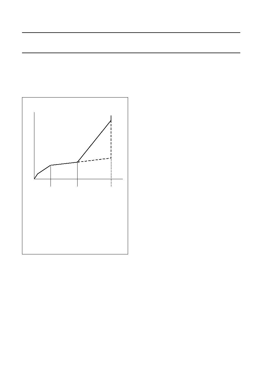
Fig.7
General form of the DC mask as a function
of the regulation mode.
(1) Low voltage area.
(2) Small slope (determined by R
SLPE
).
(3) Small slope (dashed line; determined by R
SLPE
) in voltage
regulation mode.
High slope (full line; determined by R
SLPE
, R
LVI
and R
RGL
) in
current regulation mode.
(4) Current limitation.
handbook, halfpage
MGK710
Vline
Iline
Iprot
(4)
Iknee
Ilow
(1)
(2)
(3)
Therefore, V
CE
(TN
SW
)
R
LVI
◊
I
LVIV
= 200 mV in a typical
application (see Fig.15).
The slope
V
line
/
I
line
of the V
line
, I
line
characteristic is
R
REGV
R
SLPE.
Current regulation mode
In current regulation mode (bit CRC at logic 1), when the
line current is lower than I
knee
= 35 mA (with
Z
SET
= 619
), V
CE
(TN
SW
) is fixed by means of a 200 nA
DC constant current I
LVIV
flowing through R
LVI
. When the
line current is higher than 35 mA, an additional current
(proportional to the line current) flows through R
LVI
. As a
result, TN
SW
works as a DC voltage source increasing with
the line current. V
CE
(TN
SW
) can be calculated as follows:
Where:
I
line
= line current
R
RGL
= resistor connected at pin RGL.
In a typical application (see Fig.15), the slope
V
line
/
I
line
of the V
line
, I
line
characteristic is determined by the ratio of
the resistors connected at pins SLPE, LVI and RGL, as
follows:
.
Current limitation
Whatever the selected mode is, the line current is limited
to approximately 145 mA; this current is sensed on SLPE.
For this purpose, the external Zener diode must be
connected between pins LN and SLPE. The speech
function no longer operates in this condition.
E
LECTRONIC HOOK SWITCH CONTROL
(
PIN
EHI)
The electronic hook switch input (EHI) controls the state of
transistor TP
DARL
. When the voltage applied at pin EHI is
LOW, transistor TP
DARL
is turned off. The voltage at
pin LCC is pulled up to supply voltage (V
CC
). Transistors
TN
SW
and TN
ON-HOOK
are also turned off by means of a
pull-down resistor (R
PD
). When the voltage applied at
pin EHI is HIGH, transistor TP
DARL
is driven by the
operational amplifier at pin LCC and the regulation mode
selected is operating. An internal 165 k
pull-up resistor is
connected between pins LCC and V
CC
.
V
CE
TN
SW
(
)
R
LVI
R
SLPE
R
RGL
----------------
I
line
I
knee
≠
(
)
I
LVIV
+
◊
◊
R
REGC
R
SLPE
R
LVI
R
SLPE
R
RGL
----------------
1400
=
◊
+

1999 Jun 04
11
Philips Semiconductors
Objective specification
Cordless telephone line interface
UBA1706
Input EHI can also be used for pulse dialling or register
recall (timed loop break). During line breaks (the voltage at
pin EHI is LOW or open-circuit), the voltage regulator is
switched off and the capacitor at pin REG is internally
disconnected to prevent its discharge. As a result, the
voltage stabilizer will have negligible switch-on delay after
line interruptions. This minimizes the contribution of the IC
to the current waveform during pulse dialling or register
recall.
When the UBA1706 is in power-down mode (bit PD at
logic 1), transistor TP
DARL
is forced off whatever the
voltage applied at pin EHI.
S
ET IMPEDANCE
In the audio frequency range, the dynamic impedance
between pins LN and GND (illustrated in Fig.8) is mainly
determined by the Z
SET
impedance. The impedance
introduced by the external TN
SW
transistor connected
between pins GND and LN
-
is negligible.
T
RANSMIT AMPLIFIER
(
PINS
TXI+
AND
TXI
-
)
The UBA1706 has symmetrical transmit inputs TXI+ and
TXI
-
. The input impedance between pins TXI+ or TXI
-
and
GND is 21 k
. The voltage gain from pins TXI+ or TXI
-
to
pin LN is set at 11.6 dB with 600
line load (Z
line
) and
619
set impedance. The inputs are biased at
2
◊
V
d
1.4 V, with V
d
representing the diode voltage.
AGC is provided on this amplifier for line loss
compensation.
R
ECEIVE AMPLIFIER
(
PINS
RXI
AND
RXO;
BIT
RXM)
The receive amplifier (see Fig.9) has one input (RXI) and
one output (RXO). The input impedance between
pins RXI and GND is 21 k
.
The rail-to-rail output stage is designed to drive a 500
µ
A
peak current. The output impedance at pin RXO is
approximately 100
.
The voltage gain from pin RXI to pin RXO is set at 37.9 dB.
This gain value compensates typically the attenuation of
the anti-sidetone network (see Fig.10). The output and the
input are biased at 2
◊
V
d
1.4 V.
AGC is provided on this amplifier for line loss
compensation. This amplifier can be muted by activating
the receive mute function (bit RXM at logic 1).
Fig.8
Equivalent impedance between
pins LN and GND.
L
eq
= C
REG
◊
R
SLPE
◊
R
P
R
P
= internal resistance = 35 k
.
handbook, halfpage
LN
GND
SLPE
RSLPE
CREG
REG
ZSET
4.7
µ
F
619
10
RP
Vref
LEQ
MGL215
Fig.9 Receive amplifier.
Bit names are given in italics.
handbook, full pagewidth
FCA035
V
I
V
I
RXM
2Vd
2Vd
from AGC
RXI
RXO
UBA1706
1999 Jun 04
12
Philips Semiconductors
Objective specification
Cordless telephone line interface
UBA1706
S
IDETONE SUPPRESSION
The UBA1706 anti-sidetone network comprising
Z
SET
//Z
line
, R
ast1
, R
ast2
, R
ast3
, R
SLPE
and Z
bal
(see Fig.10)
suppresses the transmitted signal in the received signal.
Maximum compensation is obtained when the following
conditions are fulfilled:
R
SLPE
◊
R
ast1
= Z
SET
◊
(R
ast2
+ R
ast3
)
Z
bal
= k
◊
Z
line
The scale factor `k' is chosen to meet the compatibility with
a standard capacitor from the E6 or E12 range for Z
bal
.
In practice, Z
line
varies considerably with the line type and
the line length.
k
R
ast2
R
ast3
R
SLPE
+
(
)
◊
(
)
R
ast1
R
SLPE
◊
(
)
--------------------------------------------------------------------
=
Therefore, the value chosen for Z
bal
should be for an
average line length, which gives satisfactory sidetone
suppression with short and long lines.
The suppression also depends on the accuracy of the
match between Z
bal
and the impedance of the average
line.
The anti-sidetone network for the UBA1706 (see Fig.15)
attenuates the receiving signal from the line by 38 dB
before it enters the receiving amplifier. The attenuation is
almost constant over the whole audio frequency range.
A Wheatstone bridge configuration (see Fig.11) may also
be used.
More information on the balancing of an anti-sidetone
bridge can be obtained in our publication
"Applications
Handbook for Wired Telecom Systems, IC03b".
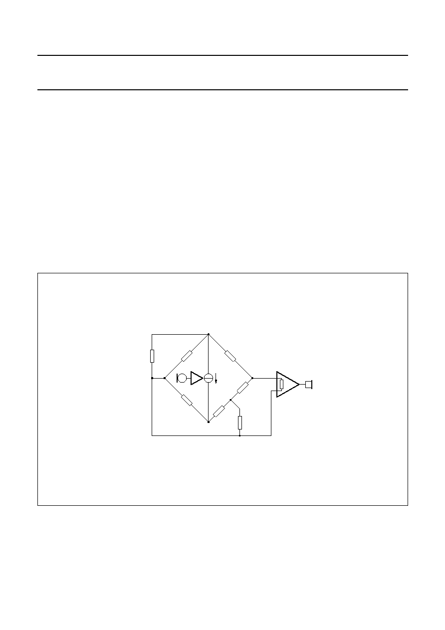
Fig.10 Equivalent circuit of UBA1706 anti-sidetone bridge.
handbook, full pagewidth
MGL216
Im
ZRXI
RXI
Rast1
Rast3
Rast2
SLPE
RSLPE
GND
Zline
ZSET
LN
Zbal

1999 Jun 04
13
Philips Semiconductors
Objective specification
Cordless telephone line interface
UBA1706
Fig.11 Equivalent circuit of an anti-sidetone network in a Wheatstone bridge configuration.
handbook, full pagewidth
MGL217
Im
ZRXI
RXI
Zbal
Rast1
SLPE
RSLPE
GND
Zline
ZSET
LN
RA
A
UTOMATIC GAIN CONTROL
(
PIN
AGC;
BITS
RAGC1,
RAGC2, SAGC
AND
AGC)
The UBA1706 performs automatic line loss compensation.
The AGC varies the gain of the transmit amplifier and the
gain of the receive amplifier in accordance with the DC line
current. The control range is 6.5 dB (which corresponds
roughly to a line length of 5.5 km for a 0.5 mm diameter
twisted-pair copper cable with a DC resistance of
176
/km and an average attenuation of 1.2 dB/km).
When the line current is greater than I
stop
, the voltage
gains are minimum. When the line current is less than I
start
,
the voltage gains are maximum.
When the AGC pin is connected to pin GND, the start line
current (I
start
) can be chosen between 22.5 and 29.5 mA
via bits RAGC1 and RAGC2 through the serial interface.
Two values for the I
stop
/I
start
ratio (slope of the AGC) are
possible via bit SAGC through the serial interface. When
bit SAGC is at logic 0 then I
stop
= 2.7
◊
I
start
(optimized for
voltage regulation mode). When SAGC is at logic 1 then
I
stop
= 1.9
◊
I
start
(optimized for current regulation mode).
An external resistor R
AGC
(connected between pins GND
and AGC) enables the I
start
and I
stop
line currents to be
increased (the ratio between I
start
and I
stop
is not affected
by this external resistor). Therefore, internal and external
adjustments of the AGC allow optimization of the IC for
many configurations of exchange supply voltage and
feeding bridge resistance.
Part of the line current flows into the Z
SET
impedance
network. The IC has been optimized for Z
SET
= 619
.
Changing this 619
value slightly modifies I
stop
and I
start
line currents as well as the value of the two AGC slopes.
The AGC function can be disabled by setting the AGC bit
to logic 0 via the serial interface or by leaving pin AGC
open-circuit. In this case, both of the voltage gains are
maximum.

1999 Jun 04
14
Philips Semiconductors
Objective specification
Cordless telephone line interface
UBA1706
General purpose switches (pins SWI1 and SWI2; bits
SWC1 and SWC2)
The UBA1706 is equipped with two general purpose
open-collector switches, which short circuit pins SWI1 and
SWI2 to ground. These switches are controlled by bits
SWC1 and SWC2, respectively, and have an operating
voltage limited to 12 V. The outputs have to be current
biased. For a bias current between 2 and 20 mA, the
AC impedance is 30
maximum.
Serial interface (pins DATA, CLK and EN)
A simple 3-wire unidirectional serial bus is used to program
the circuit. The three wires of the bus are EN, CLK and
DATA. The data sent to the device is loaded in bursts
framed by EN. Programming clock edges (falling edges)
and their appropriate data bits are ignored until EN goes
HIGH. The programmed information is loaded into the
addressed register when EN returns to LOW or left
open-circuit.
During normal operation, EN should be kept LOW. Only
the last seven bits serially clocked into the device are
retained within the programming register.
Additional leading bits are ignored and no check is made
on the number of clock pulses. New programming data can
always be captured during global power-down (bit PD at
logic 1).
Data is entered with the most significant bit first. The
leading six bits make up the data field (bits D0 to D5) while
the trailing two bits are the address field (bits ADO and
AD1). The first bit entered is D5, the last bit AD0. This
organisation allows the transmission of only the number of
bits of the addressed register.
Figure 13 shows the serial timing diagram. Table 1 gives
the list of registers.
When the supply voltage V
CC
drops below 2.5 V, all
register files are set to the initial state (see Table 1)
defined by the power-up reset. At start-up, the circuit is in
power-down mode.
When the IC is used in a noisy environment, it is advised
to periodically refresh the content of registers.

1999 Jun 04
15
Philips Semiconductors
Objective specification
Cordless telephone line interface
UBA1706
Table 1
Register description; note 1
Notes
1. For full software compatibility, the registers have the same addresses as for the UBA1707.
2. See Section "Automatic gain control (pin AGC; bits RAGC1, RAGC2, SAGC and AGC)".
BIT
NAME
FUNCTION
POLARITY
DATA
ADDRESS
STATE AT
POWER-UP
RESET
Register 0: general purpose switches state and DC mask regulation mode
SWC1
SWI1 output connection
0: SWI1 switched-off
D0
(AD1, AD0) = (0,0)
0
1: SWI1 switched-on
SWC2
SWI2 output connection
0: SWI2 switched-off
D1
0
1: SWI2 switched-on
un
unused
must be set to logic 0
D2
0
un
unused
must be set to logic 0
D3
0
CRC
current regulation mode
0: voltage regulation
D4
0
1: current regulation
Register 1: automatic gain control
RAGC1
AGC range selection 1
D0
(AD1, AD0) = (0,1)
0
RAGC2
AGC range selection 2
D1
0
SAGC
AGC slope selection
0: 2.7 type slope; note 2
D2
0
1: 1.9 type slope; note 2
AGC
line loss compensation mode
0: AGC inhibited
D3
0
1: AGC enabled
Register 2
unused, in case of programming register 2 data must be set to: 000100 (D5; D0)
(AD1, AD0) = (1,0)
-
Register 3: mute functions and power-down
un
unused
must be set to logic 1
D0
(AD1, AD0) = (1,1)
0
RXM
receive amplifier mute
0: amplifier enabled
D1
0
1: amplifier muted
PD
reduced consumption mode
0: normal operating mode
D2
1
1: power-down mode
un
unused
must be set to logic 1
D3
0
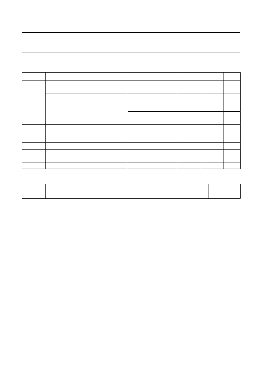
1999 Jun 04
16
Philips Semiconductors
Objective specification
Cordless telephone line interface
UBA1706
LIMITING VALUES
In accordance with the Absolute Maximum Rating System (IEC 134).
THERMAL CHARACTERISTICS
SYMBOL
PARAMETER
CONDITIONS
MIN.
MAX.
UNIT
V
CC
supply voltage
GND
-
0.4 5.5
V
V
LN
positive continuous line voltage on pin LN
GND
-
0.4 12.0
V
repetitive line voltage during switch-on or
line interruption
GND
-
0.4 13.2
V
V
SWIn
voltage on pins SWI1 and SWI2
continuous
GND
-
0.4 12.0
V
during switching
GND
-
0.4 13.2
V
V
n(max)
maximum voltage on all other pins
GND
-
0.4 V
CC
+ 0.4
V
I
LN
current sunk by pin LN
see Fig.12
-
150
mA
I
SWIn
continuous current sunk by pins SWI1 and
SWI2
bit SWCn = 1
-
20
mA
P
tot
total power dissipation
T
amb
= 75
∞
C; see Fig.12
-
454
mW
T
stg
IC storage temperature
-
40
+125
∞
C
T
amb
ambient temperature
-
25
+75
∞
C
T
j
junction temperature
-
+125
∞
C
SYMBOL
PARAMETER
CONDITIONS
VALUE
UNIT
R
th(j-a)
thermal resistance from junction to ambient in free air
100
K/W

1999 Jun 04
17
Philips Semiconductors
Objective specification
Cordless telephone line interface
UBA1706
Fig.12 Safe operating area.
The line current value can be calculated from the I
LN
value as follows:
where R
SET
is the resistive part of Z
SET
.
I
line
I
LN
R
SET
R
SLPE
+
(
)
V
LN
V
SLPE
≠
+
◊
R
SET
----------------------------------------------------------------------------------------------
=
handbook, full pagewidth
2
3
4
5
6
7
8
9
10
11
12.
30
50
70
90
110
130
150
ILN
(mA)
VLN - VSLPE (V)
(4)
(3)
(2)
(1)
FCA036
(1) T
amb
= 45
∞
C; P
tot
= 727 mW
(2) T
amb
= 55
∞
C; P
tot
= 636 mW
(3) T
amb
= 65
∞
C; P
tot
= 545 mW
(4) T
amb
= 75
∞
C; P
tot
= 454 mW

1999 Jun 04
18
Philips Semiconductors
Objective specification
Cordless telephone line interface
UBA1706
CHARACTERISTICS
I
line
= 15 mA; V
CC
= 3.3 V; R
SLPE
= 10
; AGC pin connected to GND; Z
line
= 600
; Z
SET
= 619
; EHI = HIGH;
f = 1 kHz; T
amb
= 25
∞
C; bit AGC at logic 1, all other configuration bits at logic 0; measured in test circuit of Fig.14;
unless otherwise specified.
SYMBOL
PARAMETER
CONDITIONS
MIN.
TYP.
MAX.
UNIT
Supply (pins V
CC
and GND; bit PD)
V
CC
supply voltage
3.0
-
5.5
V
I
CC
current consumption from
pin V
CC
-
2.2
3.2
mA
I
CC(pd)
current consumption from
pin V
CC
in power-down mode
bit PD = 1
-
110
150
µ
A
Line interface (pins LN, SLPE and REG)
DC
CHARACTERISTICS
V
ref
stabilized voltage between
pins LN and SLPE
I
line
= 11 to 140 mA
2.6
2.9
3.2
V
V
LN
DC line voltage between pins
LN and GND
I
line
= 2 mA
-
1.2
-
V
I
line
= 4 mA
-
1.8
-
V
I
line
= 15 mA
2.7
3.0
3.3
V
I
line
= 140 mA
-
4.35
-
V
V
LN(Rext)
DC line voltage between pins
LN and GND with an external
resistor R
VA
R
VA(SLPE
-
REG)
= 8 k
-
4.5
-
V
V
LN(T)
DC line voltage variation with
temperature referenced to
25
∞
C
T
amb
=
-
25 to +75
∞
C
-
8.0
-
mV
Masks regulation (pins LCC, LVI, CST and RGL; bit CRC)
DC
CHARACTERISTICS
I
LCC(max)
maximum current sunk by
pin LCC
500
-
-
µ
A
R
int(LCC)
internal resistance between
pins V
CC
and LCC
-
165
-
k
Voltage regulation mode
I
LVIV
current sourced from pin LVI
bit CRC = 0
-
200
-
nA
Current regulation mode
I
knee
start line current for current
regulation mode
bit CRC = 1
-
35
-
mA
R
REGC
DC mask slope in current
regulation mode
I
line
> I
knee
; R
LVI
= 1 M
;
R
RGL
= 7.15 k
; bit CRC = 1
-
1.4
-
k
Current limitation
I
prot
current limitation level
-
145
-
mA

1999 Jun 04
19
Philips Semiconductors
Objective specification
Cordless telephone line interface
UBA1706
Electronic hook-switch control (pin EHI)
V
IH
HIGH-level input voltage
2.3
-
V
CC
+ 0.4
V
V
IL
LOW-level input voltage
V
CC
= 3.0 to 5.5 V
GND
-
0.4
-
0.3V
CC
V
I
bias
input bias current
input level = HIGH
1
2
5
µ
A
Transmit amplifier (pins TXI+, TXI
-
and LN)
Z
i
input impedance
between pins TXI+ and
GND or TXI
-
and GND
-
21
-
k
between pins TXI+ and TXI
- -
36
-
k
G
v(TX)
voltage gain from TXI+/TXI
-
to LN
V
TXI
= 50 mV (RMS)
10.6
11.6
12.6
dB
G
v(TX)(f)
voltage gain variation with
frequency referenced to 1 kHz
f = 300 to 3400 Hz
-
±
0.3
-
dB
G
v(TX)(T)
voltage gain variation with
temperature referenced to
25
∞
C
T
amb
=
-
25 to +75
∞
C
-
±
0.3
-
dB
CMRR
common mode rejection ratio
-
65
-
dB
PSRR
power supply rejection ratio
-
36
-
dB
V
LN(max)(rms)
maximum sending signal
(RMS value)
I
line
= 15 mA; THD = 2%
1.2
1.4
-
V
I
line
= 4 mA; THD = 10%
-
0.26
-
V
V
iTX(max)(rms)
maximum transmit input
voltage (RMS value) for
2% THD on pin LN
I
line
= 15 mA
-
0.35
-
V
I
line
= 90 mA
-
0.75
-
V
V
no(LN)
noise output voltage at pin LN pins TXI+ and TXI
-
short-circuited through
200
in series with 10
µ
F;
psophometrically weighted
(P53 curve)
-
-
74
-
dBmp
Receive amplifier (pins RXI and RXO; bit RXM)
Z
i
input impedance between
pins RXI and GND
-
21
-
k
G
v(RX)
voltage gain from RXI to RXO
V
RXI
= 2 mV (RMS)
36.9
37.9
38.9
dB
G
v(RX)(f)
voltage gain variation with
frequency referenced to 1 kHz
f = 300 to 3400 Hz
-
±
0.2
-
dB
G
v(RX)(T)
voltage gain variation with
temperature referenced to
25
∞
C
T
amb
=
-
25 to +75
∞
C
-
±
0.3
-
dB
PSRR
power supply rejection ratio
-
68
-
dB
THD
total harmonic distortion
V
RXI
= 2 mV (RMS)
-
0.03
-
%
V
RXI
= 12.5 mV (RMS)
-
2
-
%
V
RXI
= 19.5 mV (RMS);
I
line
= 90 mA
-
2
-
%
SYMBOL
PARAMETER
CONDITIONS
MIN.
TYP.
MAX.
UNIT

1999 Jun 04
20
Philips Semiconductors
Objective specification
Cordless telephone line interface
UBA1706
V
no(RXO)(rms)
noise output voltage at
pin RXO (RMS value)
RXI open-circuit;
psophometrically weighted
(P53 curve)
-
-
81
-
dBVp
G
v(RX)(m)
voltage gain reduction from
pin RXI to RXO when muted
V
RXI
= 10 mV (RMS);
bit RXM = 1
-
80
-
dB
Automatic gain control (pin AGC; bits RAGC1, RAGC2, SAGC and AGC)
G
v(trx)
gain control range for transmit
and receive amplifiers with
respect to I
line
= 15 mA
I
line
= 90 mA
-
6.5
-
dB
I
start
highest line current for
maximum gain
bits RAGC1 = 1;
RAGC2 = 1
-
22.5
-
mA
bits RAGC1 = 1;
RAGC2 = 0
-
25
-
mA
bits RAGC1 = 0;
RAGC2 = 1
-
27
-
mA
bits RAGC1 = 0;
RAGC2 = 0
-
29.5
-
mA
I
stop
lowest line current for
minimum gain when
I
start
= 23 mA
bits SAGC = 0; RAGC1 = 1;
RAGC2 = 1
-
62
-
mA
bits SAGC = 1; RAGC1 = 1;
RAGC2 = 1
-
43
-
mA
G
v(trxoff)
gain variation for transmit and
receive amplifiers when AGC
is off
bit AGC = 0;
I
line
= 15 to 140 mA
-
-
±
0.2
dB
Switches (pins SWI1 and SWI2; bits SWC1 and SWC2)
Z
i(off)
AC impedance between pins
SWIn and GND when not
selected
bit SWCn = 0
700
-
-
k
Z
i(on)
AC impedance between pins
SWIn and GND when
selected
2 mA < I
SWIn
< 20 mA;
bit SWCn = 1
-
-
30
Serial interface (pins DATA, CLK and EN)
V
IH
HIGH-level input voltage
2.3
-
V
CC
+ 0.4
V
V
IL
LOW-level input voltage
V
CC
= 3 to 5.5 V
GND
-
0.4
-
0.3V
CC
V
I
bias
input bias current
input level = HIGH
1
2
5
µ
A
C
i
input capacitance at pins
DATA, CLK and EN
-
4
-
pF
SYMBOL
PARAMETER
CONDITIONS
MIN.
TYP.
MAX.
UNIT

1999 Jun 04
21
Philips Semiconductors
Objective specification
Cordless telephone line interface
UBA1706
SERIAL BUS TIMING CHARACTERISTICS
V
CC
= 3.3 V; T
amb
= 25
∞
C; unless otherwise specified.
SYMBOL
PARAMETER
MIN.
MAX.
UNIT
Serial programming clock; pin CLK
f
clk
clock frequency
0
300
kHz
Enable programming; pin EN
t
START
delay to falling clock edge
1
-
µ
s
t
END
delay from last rising clock edge
0.1
-
µ
s
t
W(min)
minimum inactive pulse width
1.5
-
µ
s
t
SU; EN
enable set-up time to next clock edge
0.1
-
µ
s
Serial data; pin DATA
t
SU; DATA
input data to clock set-up time
2
-
µ
s
t
HD; DATA
input data to clock hold time
2
-
µ
s
Fig.13 Serial bus timing diagram.
handbook, full pagewidth
MGK716
tSU;DATA
1/fclk
tSU;EN
tEND
tW
tHD;DATA
tSTART
CLK
DATA
EN
D5
D4
AD1
AD0
1999
Jun
04
22
Philips Semiconductors
Objective specification
Cordless telephone line interface
UBA1706
This text is here in white to force landscape pages to be rotated correctly when browsing through the pdf in the Acrobat reader.This text is here in
_
white to force landscape pages to be rotated correctly when browsing through the pdf in the Acrobat reader.This text is here inThis text is here in
white to force landscape pages to be rotated correctly when browsing through the pdf in the Acrobat reader. white to force landscape pages to be ...
TEST AND APPLICA
TION INFORMA
TION
handbook, full pagewidth
FCA037
LN
GND
SWI1
EHI
SWI2
1
19
17
18
10
DATA
11
EN
12
CLK
13
LCC
CST
REG
LVI
5
6
3
2
AGC
8
RGL
4
24
TXI
+
15
TXI
-
14
VCC
ICC
21
RXI
9
RXO
from
microcontroller
UBA1706
CLVI
470 pF
Cline
100
µ
F
CEMC
10 nF
CREG
4.7
µ
F
RLVI
1 M
RRGL
7.15 k
SLPE
RSLPE
10
ZSET
619
Zline
600
CRXI
220 nF
CCST
27 pF
VRXI
TNON-HOOK
MPSA42
TPDARL
MPSA92
100 k
RON-HOOK
Dprot
1N4148
RPD
20 k
DSW
1N4148
TNSW
BUX86
VVCC
VLN
Iline
VTXI
CVCC
10
µ
F
CLCC
6.8 pF
7
Fig.14 Test circuit.

1999
Jun
04
23
Philips Semiconductors
Objective specification
Cordless telephone line interface
UBA1706
This text is here in white to force landscape pages to be rotated correctly when browsing through the pdf in the Acrobat reader.This text is here in
_
white to force landscape pages to be rotated correctly when browsing through the pdf in the Acrobat reader.This text is here inThis text is here in
white to force landscape pages to be rotated correctly when browsing through the pdf in the Acrobat reader. white to force landscape pages to be ...
handbook, full pagewidth
FCA038
LN
SWI2
SWI1
1
17
18
RXI
9
RXO
7
LCC
CST
REG
LVI
5
6
3
2
AGC
8
RGL
4
GND
19
TXI
+
15
TXI
-
14
VCC
ICC
21
SLPE
24
EHI
DATA
10
EN
CLK
11
13
UBA1706
CRXI
100 nF
CLVI
(2)
470 pF
CVCC
10
µ
F
CEMC
(3)
10 nF
CREG
4.7
µ
F
CRXO
RSLPE
Rast3
392
RLVI
1 M
RRGL
7.15 k
ZSET
619
10
Zbal
Rast2
3.92 k
Rast1
260 k
BZX79C8V2
CTXIP
100 nF
CTXIM
100 nF
12
CCST
27pF
TNON-HOOK
MPSA42
TPDARL
MPSA92
100 k
RON-HOOK
Dprot
1N4148
RPD
20 k
DSW
1N4148
TNSW
BUX86
(MPSA42
(1)
)
VVCC
VLN
BRIDGE
4
◊
BAS11
a/b
b/a
BOD
BR211-240
CLCC
(4)
6.8 pF
M
I
C
R
O
C
O
N
T
R
O
L
L
E
R
Fig.15 Typical application.
(1) In case of low line current in voltage regulation mode.
(2) Only required in current regulation mode.
(3) To improve EMC performance; necessary for stability.
(4) To improve stability only in current regulation mode.
1999 Jun 04
24
Philips Semiconductors
Objective specification
Cordless telephone line interface
UBA1706
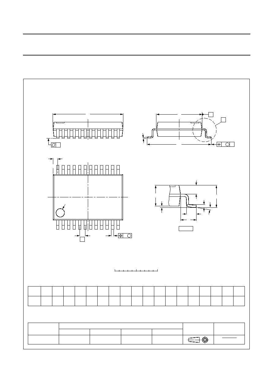
PACKAGES OUTLINE
UNIT
A
1
A
2
A
3
b
p
c
D
(1)
E
(1)
(1)
e
H
E
L
L
p
Q
Z
y
w
v
REFERENCES
OUTLINE
VERSION
EUROPEAN
PROJECTION
ISSUE DATE
IEC
JEDEC
EIAJ
mm
0.21
0.05
1.80
1.65
0.38
0.25
0.20
0.09
8.4
8.0
5.4
5.2
0.65
1.25
7.9
7.6
0.9
0.7
0.8
0.4
8
0
o
o
0.13
0.1
0.2
DIMENSIONS (mm are the original dimensions)
Note
1. Plastic or metal protrusions of 0.20 mm maximum per side are not included.
1.03
0.63
SOT340-1
MO-150AG
93-09-08
95-02-04
X
w
M
A
A
1
A
2
b
p
D
H
E
L
p
Q
detail X
E
Z
e
c
L
v
M
A
(A )
3
A
1
12
24
13
0.25
y
pin 1 index
0
2.5
5 mm
scale
SSOP24: plastic shrink small outline package; 24 leads; body width 5.3 mm
SOT340-1
A
max.
2.0

1999 Jun 04
25
Philips Semiconductors
Objective specification
Cordless telephone line interface
UBA1706
SOLDERING
Introduction to soldering surface mount packages
This text gives a very brief insight to a complex technology.
A more in-depth account of soldering ICs can be found in
our
"Data Handbook IC26; Integrated Circuit Packages"
(document order number 9398 652 90011).
There is no soldering method that is ideal for all surface
mount IC packages. Wave soldering is not always suitable
for surface mount ICs, or for printed-circuit boards with
high population densities. In these situations reflow
soldering is often used.
Reflow soldering
Reflow soldering requires solder paste (a suspension of
fine solder particles, flux and binding agent) to be applied
to the printed-circuit board by screen printing, stencilling or
pressure-syringe dispensing before package placement.
Several methods exist for reflowing; for example,
infrared/convection heating in a conveyor type oven.
Throughput times (preheating, soldering and cooling) vary
between 100 and 200 seconds depending on heating
method.
Typical reflow peak temperatures range from
215 to 250
∞
C. The top-surface temperature of the
packages should preferable be kept below 230
∞
C.
Wave soldering
Conventional single wave soldering is not recommended
for surface mount devices (SMDs) or printed-circuit boards
with a high component density, as solder bridging and
non-wetting can present major problems.
To overcome these problems the double-wave soldering
method was specifically developed.
If wave soldering is used the following conditions must be
observed for optimal results:
∑
Use a double-wave soldering method comprising a
turbulent wave with high upward pressure followed by a
smooth laminar wave.
∑
For packages with leads on two sides and a pitch (e):
≠ larger than or equal to 1.27 mm, the footprint
longitudinal axis is preferred to be parallel to the
transport direction of the printed-circuit board;
≠ smaller than 1.27 mm, the footprint longitudinal axis
must be parallel to the transport direction of the
printed-circuit board.
The footprint must incorporate solder thieves at the
downstream end.
∑
For packages with leads on four sides, the footprint must
be placed at a 45
∞
angle to the transport direction of the
printed-circuit board. The footprint must incorporate
solder thieves downstream and at the side corners.
During placement and before soldering, the package must
be fixed with a droplet of adhesive. The adhesive can be
applied by screen printing, pin transfer or syringe
dispensing. The package can be soldered after the
adhesive is cured.
Typical dwell time is 4 seconds at 250
∞
C.
A mildly-activated flux will eliminate the need for removal
of corrosive residues in most applications.
Manual soldering
Fix the component by first soldering two
diagonally-opposite end leads. Use a low voltage (24 V or
less) soldering iron applied to the flat part of the lead.
Contact time must be limited to 10 seconds at up to
300
∞
C.
When using a dedicated tool, all other leads can be
soldered in one operation within 2 to 5 seconds between
270 and 320
∞
C.
1999 Jun 04
26
Philips Semiconductors
Objective specification
Cordless telephone line interface
UBA1706
Suitability of surface mount IC packages for wave and reflow soldering methods
Notes
1. All surface mount (SMD) packages are moisture sensitive. Depending upon the moisture content, the maximum
temperature (with respect to time) and body size of the package, there is a risk that internal or external package
cracks may occur due to vaporization of the moisture in them (the so called popcorn effect). For details, refer to the
Drypack information in the
"Data Handbook IC26; Integrated Circuit Packages; Section: Packing Methods".
2. These packages are not suitable for wave soldering as a solder joint between the printed-circuit board and heatsink
(at bottom version) can not be achieved, and as solder may stick to the heatsink (on top version).
3. If wave soldering is considered, then the package must be placed at a 45
∞
angle to the solder wave direction.
The package footprint must incorporate solder thieves downstream and at the side corners.
4. Wave soldering is only suitable for LQFP, TQFP and QFP packages with a pitch (e) equal to or larger than 0.8 mm;
it is definitely not suitable for packages with a pitch (e) equal to or smaller than 0.65 mm.
5. Wave soldering is only suitable for SSOP and TSSOP packages with a pitch (e) equal to or larger than 0.65 mm; it is
definitely not suitable for packages with a pitch (e) equal to or smaller than 0.5 mm.
DEFINITIONS
LIFE SUPPORT APPLICATIONS
These products are not designed for use in life support appliances, devices, or systems where malfunction of these
products can reasonably be expected to result in personal injury. Philips customers using or selling these products for
use in such applications do so at their own risk and agree to fully indemnify Philips for any damages resulting from such
improper use or sale.
PACKAGE
SOLDERING METHOD
WAVE
REFLOW
(1)
BGA, SQFP
not suitable
suitable
HLQFP, HSQFP, HSOP, HTSSOP, SMS not suitable
(2)
suitable
PLCC
(3)
, SO, SOJ
suitable
suitable
LQFP, QFP, TQFP
not recommended
(3)(4)
suitable
SSOP, TSSOP, VSO
not recommended
(5)
suitable
Data sheet status
Objective specification
This data sheet contains target or goal specifications for product development.
Preliminary specification
This data sheet contains preliminary data; supplementary data may be published later.
Product specification
This data sheet contains final product specifications.
Limiting values
Limiting values given are in accordance with the Absolute Maximum Rating System (IEC 134). Stress above one or
more of the limiting values may cause permanent damage to the device. These are stress ratings only and operation
of the device at these or at any other conditions above those given in the Characteristics sections of the specification
is not implied. Exposure to limiting values for extended periods may affect device reliability.
Application information
Where application information is given, it is advisory and does not form part of the specification.

1999 Jun 04
27
Philips Semiconductors
Objective specification
Cordless telephone line interface
UBA1706
NOTES

© Philips Electronics N.V.
SCA
All rights are reserved. Reproduction in whole or in part is prohibited without the prior written consent of the copyright owner.
The information presented in this document does not form part of any quotation or contract, is believed to be accurate and reliable and may be changed
without notice. No liability will be accepted by the publisher for any consequence of its use. Publication thereof does not convey nor imply any license
under patent- or other industrial or intellectual property rights.
Internet: http://www.semiconductors.philips.com
1999
65
Philips Semiconductors ≠ a worldwide company
Netherlands: Postbus 90050, 5600 PB EINDHOVEN, Bldg. VB,
Tel. +31 40 27 82785, Fax. +31 40 27 88399
New Zealand: 2 Wagener Place, C.P.O. Box 1041, AUCKLAND,
Tel. +64 9 849 4160, Fax. +64 9 849 7811
Norway: Box 1, Manglerud 0612, OSLO,
Tel. +47 22 74 8000, Fax. +47 22 74 8341
Pakistan: see Singapore
Philippines: Philips Semiconductors Philippines Inc.,
106 Valero St. Salcedo Village, P.O. Box 2108 MCC, MAKATI,
Metro MANILA, Tel. +63 2 816 6380, Fax. +63 2 817 3474
Poland: Ul. Lukiska 10, PL 04-123 WARSZAWA,
Tel. +48 22 612 2831, Fax. +48 22 612 2327
Portugal: see Spain
Romania: see Italy
Russia: Philips Russia, Ul. Usatcheva 35A, 119048 MOSCOW,
Tel. +7 095 755 6918, Fax. +7 095 755 6919
Singapore: Lorong 1, Toa Payoh, SINGAPORE 319762,
Tel. +65 350 2538, Fax. +65 251 6500
Slovakia: see Austria
Slovenia: see Italy
South Africa: S.A. PHILIPS Pty Ltd., 195-215 Main Road Martindale,
2092 JOHANNESBURG, P.O. Box 58088 Newville 2114,
Tel. +27 11 471 5401, Fax. +27 11 471 5398
South America: Al. Vicente Pinzon, 173, 6th floor,
04547-130 S√O PAULO, SP, Brazil,
Tel. +55 11 821 2333, Fax. +55 11 821 2382
Spain: Balmes 22, 08007 BARCELONA,
Tel. +34 93 301 6312, Fax. +34 93 301 4107
Sweden: Kottbygatan 7, Akalla, S-16485 STOCKHOLM,
Tel. +46 8 5985 2000, Fax. +46 8 5985 2745
Switzerland: Allmendstrasse 140, CH-8027 ZÐRICH,
Tel. +41 1 488 2741 Fax. +41 1 488 3263
Taiwan: Philips Semiconductors, 6F, No. 96, Chien Kuo N. Rd., Sec. 1,
TAIPEI, Taiwan Tel. +886 2 2134 2886, Fax. +886 2 2134 2874
Thailand: PHILIPS ELECTRONICS (THAILAND) Ltd.,
209/2 Sanpavuth-Bangna Road Prakanong, BANGKOK 10260,
Tel. +66 2 745 4090, Fax. +66 2 398 0793
Turkey: Yukari Dudullu, Org. San. Blg., 2.Cad. Nr. 28 81260 Umraniye,
ISTANBUL, Tel. +90 216 522 1500, Fax. +90 216 522 1813
Ukraine: PHILIPS UKRAINE, 4 Patrice Lumumba str., Building B, Floor 7,
252042 KIEV, Tel. +380 44 264 2776, Fax. +380 44 268 0461
United Kingdom: Philips Semiconductors Ltd., 276 Bath Road, Hayes,
MIDDLESEX UB3 5BX, Tel. +44 181 730 5000, Fax. +44 181 754 8421
United States: 811 East Arques Avenue, SUNNYVALE, CA 94088-3409,
Tel. +1 800 234 7381, Fax. +1 800 943 0087
Uruguay: see South America
Vietnam: see Singapore
Yugoslavia: PHILIPS, Trg N. Pasica 5/v, 11000 BEOGRAD,
Tel. +381 11 62 5344, Fax.+381 11 63 5777
For all other countries apply to: Philips Semiconductors,
International Marketing & Sales Communications, Building BE-p, P.O. Box 218,
5600 MD EINDHOVEN, The Netherlands, Fax. +31 40 27 24825
Argentina: see South America
Australia: 34 Waterloo Road, NORTH RYDE, NSW 2113,
Tel. +61 2 9805 4455, Fax. +61 2 9805 4466
Austria: Computerstr. 6, A-1101 WIEN, P.O. Box 213,
Tel. +43 1 60 101 1248, Fax. +43 1 60 101 1210
Belarus: Hotel Minsk Business Center, Bld. 3, r. 1211, Volodarski Str. 6,
220050 MINSK, Tel. +375 172 20 0733, Fax. +375 172 20 0773
Belgium: see The Netherlands
Brazil: see South America
Bulgaria: Philips Bulgaria Ltd., Energoproject, 15th floor,
51 James Bourchier Blvd., 1407 SOFIA,
Tel. +359 2 68 9211, Fax. +359 2 68 9102
Canada: PHILIPS SEMICONDUCTORS/COMPONENTS,
Tel. +1 800 234 7381, Fax. +1 800 943 0087
China/Hong Kong: 501 Hong Kong Industrial Technology Centre,
72 Tat Chee Avenue, Kowloon Tong, HONG KONG,
Tel. +852 2319 7888, Fax. +852 2319 7700
Colombia: see South America
Czech Republic: see Austria
Denmark: Sydhavnsgade 23, 1780 COPENHAGEN V,
Tel. +45 33 29 3333, Fax. +45 33 29 3905
Finland: Sinikalliontie 3, FIN-02630 ESPOO,
Tel. +358 9 615 800, Fax. +358 9 6158 0920
France: 51 Rue Carnot, BP317, 92156 SURESNES Cedex,
Tel. +33 1 4099 6161, Fax. +33 1 4099 6427
Germany: Hammerbrookstraþe 69, D-20097 HAMBURG,
Tel. +49 40 2353 60, Fax. +49 40 2353 6300
Hungary: see Austria
India: Philips INDIA Ltd, Band Box Building, 2nd floor,
254-D, Dr. Annie Besant Road, Worli, MUMBAI 400 025,
Tel. +91 22 493 8541, Fax. +91 22 493 0966
Indonesia: PT Philips Development Corporation, Semiconductors Division,
Gedung Philips, Jl. Buncit Raya Kav.99-100, JAKARTA 12510,
Tel. +62 21 794 0040 ext. 2501, Fax. +62 21 794 0080
Ireland: Newstead, Clonskeagh, DUBLIN 14,
Tel. +353 1 7640 000, Fax. +353 1 7640 200
Israel: RAPAC Electronics, 7 Kehilat Saloniki St, PO Box 18053,
TEL AVIV 61180, Tel. +972 3 645 0444, Fax. +972 3 649 1007
Italy: PHILIPS SEMICONDUCTORS, Piazza IV Novembre 3,
20124 MILANO, Tel. +39 02 67 52 2531, Fax. +39 02 67 52 2557
Japan: Philips Bldg 13-37, Kohnan 2-chome, Minato-ku,
TOKYO 108-8507, Tel. +81 3 3740 5130, Fax. +81 3 3740 5057
Korea: Philips House, 260-199 Itaewon-dong, Yongsan-ku, SEOUL,
Tel. +82 2 709 1412, Fax. +82 2 709 1415
Malaysia: No. 76 Jalan Universiti, 46200 PETALING JAYA, SELANGOR,
Tel. +60 3 750 5214, Fax. +60 3 757 4880
Mexico: 5900 Gateway East, Suite 200, EL PASO, TEXAS 79905,
Tel. +9-5 800 234 7381, Fax +9-5 800 943 0087
Middle East: see Italy
Printed in The Netherlands
465008/02/pp28
Date of release: 1999 Jun 04
Document order number:
9397 750 05276