 | –≠–ª–µ–∫—Ç—Ä–æ–Ω–Ω—ã–π –∫–æ–º–ø–æ–Ω–µ–Ω—Ç: UBA2021T | –°–∫–∞—á–∞—Ç—å:  PDF PDF  ZIP ZIP |
Document Outline
- FEATURES
- GENERAL DESCRIPTION
- QUICK REFERENCE DATA
- ORDERING INFORMATION
- BLOCK DIAGRAM
- PINNING
- FUNCTIONAL DESCRIPTION
- Introduction
- Initial start-up
- Oscillation
- Operation in the preheat mode
- Ignition state f
- Failure to ignite
- Transition to the burn state
- Feed-forward frequency
- Capacitive mode protection
- IC supply
- Minimum gate-source voltage of T1 and T2
- Frequency and change in frequency
- Ground pins
- Charge coupling
- LIMITING VALUES
- THERMAL CHARACTERISTICS
- CHARACTERISTICS
- DESIGN EQUATIONS
- APPLICATION INFORMATION
- PACKAGE OUTLINES
- SOLDERING
- DATA SHEET STATUS
- DEFINITIONS
- DISCLAIMERS

DATA SHEET
Product specification
Supersedes data of 2000 Jul 24
File under Integrated Circuits, IC11
2001 Jan 30
INTEGRATED CIRCUITS
UBA2021
630 V driver IC for CFL and TL
lamps

2001 Jan 30
2
Philips Semiconductors
Product specification
630 V driver IC for CFL and TL lamps
UBA2021
FEATURES
∑
Adjustable preheat and ignition time
∑
Adjustable preheat current
∑
Adjustable lamp power
∑
Lamp temperature stress protection at higher mains
voltages
∑
Capacitive mode protection
∑
Protection against a too-low drive voltage for the power
MOSFETs.
GENERAL DESCRIPTION
The UBA2021 is a high-voltage IC intended to drive and
control Compact Fluorescent Lamps (CFL) or fluorescent
TL-lamps. It contains a driver circuit for an external
half-bridge, an oscillator and a control circuit for starting
up, preheating, ignition, lamp burning and protection.
QUICK REFERENCE DATA
SYMBOL
PARAMETER
CONDITIONS
MIN.
TYP.
MAX.
UNIT
High voltage supply
V
FS
high side supply voltage
I
FS
< 15
µ
A; t < 0.5 s
-
-
630
V
Start-up state
V
VS(start)
oscillator start voltage
-
11.95
-
V
V
VS(stop)
oscillator stop voltage
-
10.15
-
V
I
VS(standby)
standby current
V
VS
= 11 V
-
200
-
µ
A
Preheat mode
f
start
start frequency
-
108
-
kHz
t
ph
preheat time
C
CP
= 100 nF
-
666
-
ms
V
RS(ctrl)
control voltage at pin RS
-
-
600
-
mV
Frequency sweep to ignition
f
B
bottom frequency
-
42.9
-
kHz
t
ign
ignition time
-
625
-
ms
Normal operation
f
B
bottom frequency
-
42.9
-
kHz
t
no
non-overlap time
-
1.4
-
µ
s
I
tot
total supply current
f
B
= 43 kHz
-
1
-
mA
R
G1(on)
, R
G2(on)
high and low side on resistance
-
126
-
R
G1(off)
, R
G2(off)
high and low side off resistance
-
75
-
Feed-forward
f
ff
feed-forward frequency
I
RHV
= 0.75 mA
-
63.6
-
kHz
I
RHV
= 1.0 mA
-
84.5
-
kHz
I
i(RHV)
operating range of input current at pin RHV
0
-
1000
µ
A

2001 Jan 30
3
Philips Semiconductors
Product specification
630 V driver IC for CFL and TL lamps
UBA2021
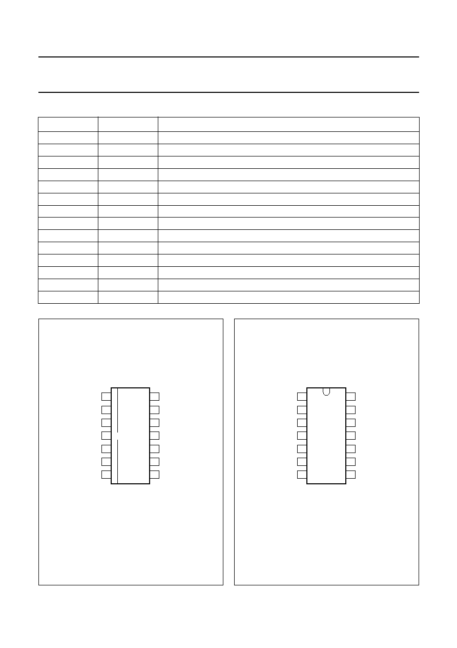
ORDERING INFORMATION
BLOCK DIAGRAM
TYPE NUMBER
PACKAGE
NAME
DESCRIPTION
VERSION
UBA2021T
SO14
plastic small outline package; 14 leads; body width 3.9 mm
SOT108-1
UBA2021P
DIP14
plastic dual in-line package; 14 leads (300 mil)
SOT27-1
handbook, full pagewidth
MGS988
UBA2021
SUPPLY
BAND GAP
REFERENCE
OSCILLATOR
TIMING
CI
2
G1
CONTROL
RS
MONITOR
NON
OVERLAP
LEVEL
SHIFTER
SB
HIGH SIDE
DRIVER
LOW SIDE
DRIVER
1
FS
14
CF
12
RREF
10
VS
n.c.
5
RHV
13
4
CP
8
RS
9
bootstrap
charging circuit
3
S1
6
G2
7
11
PGND
SGND
Fig.1 Block diagram.
2001 Jan 30
4
Philips Semiconductors
Product specification
630 V driver IC for CFL and TL lamps
UBA2021
PINNING
SYMBOL
PIN
DESCRIPTION
FS
1
high side floating supply voltage
G1
2
gate high transistor (T1)
S1
3
source high transistor (T1)
n.c.
4
high-voltage spacer, not to be connected
VS
5
low voltage supply
G2
6
gate low transistor (T2)
PGND
7
power ground
CP
8
timing/averaging capacitor
RS
9
current monitoring input
RREF
10
reference resistor
SGND
11
signal ground
CF
12
oscillator capacitor
RHV
13
start-up resistor/feed-forward resistor
CI
14
integrating capacitor
handbook, halfpage
MGS989
UBA2021T
1
2
3
4
5
6
7
8
14
13
12
11
10
9
FS
G1
S1
n.c.
VS
G2
PGND
CP
RS
RREF
SGND
CF
RHV
CI
Fig.2 Pin configuration (SO14).
handbook, halfpage
MGS990
UBA2021P
1
2
3
4
5
6
7
8
14
13
12
11
10
9
FS
G1
S1
n.c.
VS
G2
PGND
CP
RS
RREF
SGND
CF
RHV
CI
Fig.3 Pin configuration (DIP14).

2001 Jan 30
5
Philips Semiconductors
Product specification
630 V driver IC for CFL and TL lamps
UBA2021
FUNCTIONAL DESCRIPTION
Introduction
The UBA2021 is an integrated circuit for electronically
ballasted compact fluorescent lamps and their derivatives
operating with mains voltages up to 240 V (RMS). It
provides all the necessary functions for preheat, ignition
and on-state operation of the lamp. In addition to the
control function, the IC provides level shift and drive
functions for the two discrete power MOSFETs, T1 and T2
(see Fig.7).
Initial start-up
Initial start-up is achieved by charging capacitor CS9 with
the current applied to pin RHV. At start-up, MOSFET T2
conducts and T1 is non-conducting, ensuring C
boot
becomes charged. This start-up state is reached for a
supply voltage V
VS(reset)
(this is the voltage level at pin VS
at which the circuit will be reset to the initial state) and
maintained until the low voltage supply (V
VS
) reaches a
value of V
VS(start)
. The circuit is reset in the start-up state.
Oscillation
When the low voltage supply (V
VS
) has reached the value
of V
VS(start)
the circuit starts oscillating in the preheat state.
The internal oscillator is a current-controlled circuit which
generates a sawtooth waveform. The frequency of the
sawtooth is determined by the capacitor C
CF
and the
current out of pin CF (mainly set by R
RREF
). The sawtooth
frequency is twice the frequency of the signal across the
load. The IC brings MOSFETs T1 and T2 alternately into
conduction with a duty factor of approximately 50%.
Figure 4 represents the timing of the IC. The circuit block
'non-overlap' generates a non-overlap time t
no
that
ensures conduction periods of exclusively T1 or T2. Time
t
no
is dependent on the reference current I
RREF
.
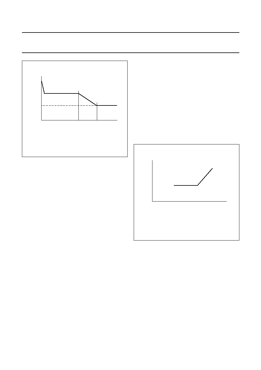
Operation in the preheat mode
The circuit starts oscillating at approximately 2.5
◊
f
B
(108 kHz). The frequency gradually decreases until a
defined value of current I
shunt
is reached (see Fig.5). The
slope of the decrease in frequency is determined by
capacitor C
CI
. The frequency during preheating is
approximately 90 kHz. This frequency is well above the
resonant frequency of the load, which means that the lamp
is off; the load consists of L2, C5 and the electrode
resistance only. The preheat time is determined by
capacitor C
CP
. The circuit can be locked in the preheat
state by connecting pin CP to ground. During preheating,
the circuit monitors the load current by measuring the
voltage drop over external resistor R
shunt
at the end of
conduction of T2 with decision level V
RS(ctrl)
. The
frequency is decreased as long as V
RS
> V
RS(ctrl)
. The
frequency is increased for V
RS
< V
RS(ctrl)
.
handbook, halfpage
MGS991
0
0
0
0
time
start-up
V(G1-S1)
V(G2)
tno
tno
internal
clock
VCF
Fig.4 Oscillator timing.
2001 Jan 30
6
Philips Semiconductors
Product specification
630 V driver IC for CFL and TL lamps
UBA2021
Ignition state
The RS monitoring function changes from V
RS(ctrl)
regulation to capacitive mode protection at the end of the
preheat time. Normally this results in a further frequency
decrease down to the bottom frequency f
B
(approximately
43 kHz). The rate of change of frequency in the ignition
state is less than that in the preheat mode. During the
downward frequency sweep, the circuit sweeps through
the resonant frequency of the load. A high voltage then
appears across the lamp. This voltage normally ignites the
lamp.
Failure to ignite
Excessive current levels may occur if the lamp fails to
ignite. The IC does not limit these currents in any manner.
Transition to the burn state
Assuming that the lamp has ignited during the downward
frequency sweep, the frequency normally decreases to the
bottom frequency. The IC can transit to the burn state in
two ways:
1. In the event that the bottom frequency is not reached,
transition is made after reaching the ignition time t
ign
.
2. As soon as the bottom frequency is reached.
The bottom frequency is determined by R
RREF
and C
CF
.
Feed-forward frequency
Above a defined voltage level the oscillation frequency
also depends on the supply voltage of the half-bridge
(see Fig.6). The current for the current-controlled oscillator
is in the feed-forward range derived from the current
through R
RHV
. The feed-forward frequency is proportional
to the average value of the current through R
RHV
within the
operating range of I
i(RHV)
, given the lower limit set by f
B
.
For currents beyond the operating range (i.e. between
1.0 and 1.6 mA) the feed-forward frequency is clamped. In
order to prevent feed-forward of ripple on V
in
, the ripple is
filtered out. The capacitor connected to pin CP is used for
this purpose. This pin is also used in the preheat state and
the ignition state for timing (t
ph
and t
ign
).
Capacitive mode protection
When the preheat mode is completed, the IC will protect
the power circuit against losing the zero voltage switching
condition and getting too close to the capacitive mode of
operation. This is detected by monitoring voltage V
RS
at
pin RS. If the voltage is below V
RS(cap)
at the time of
turn-on of T2, then capacitive mode operation is assumed.
Consequently the frequency increases as long as the
capacitive mode is detected. The frequency decreases
down to the feed-forward frequency if no capacitive mode
is detected. Frequency modulation is achieved via pin CI.
handbook, halfpage
MGS992
time
burn state
ignition
state
preheat state
fstart
fB
Fig.5 Operation in the preheat mode.
For calculations refer to Chapter "Design equations".
handbook, halfpage
MGS993
bottom
frequency
feed-forward
range
f
(kHz)
IRHV (mA)
Fig.6 Feed-forward frequency.
For calculations refer to Chapter "Design equations".

2001 Jan 30
7
Philips Semiconductors
Product specification
630 V driver IC for CFL and TL lamps
UBA2021
IC supply
Initially, the IC is supplied from V
in
by the current through
R
RHV
. This current charges the supply capacitor CS9 via
an internal diode. As soon as V
VS
exceeds V
VS(start)
, the
circuit starts oscillating. After the preheat phase is finished,
pin RHV is connected to an internal resistor R
i(RHV)
; prior
to this, pin RHV is internally connected to pin VS. The
voltage level at pin RHV thus drops from V
VS
+ V
diode
to
I
RHV
◊
R
i(RHV)
. The capacitor CS9 at pin VS will now be
charged via the snubber capacitor CS7. Excess charge is
drained by an internal clamp that turns on at voltage
V
VS(clamp)
.
Minimum gate-source voltage of T1 and T2
The high side driver is supplied via capacitor C
boot
.
Capacitor C
boot
is charged via the bootstrap switch during
the on-periods of T2. The IC stops oscillating at a voltage
level V
VS(stop)
. Given a maximum charge consumption on
the load at pin G1 of 1 nC/V, this safeguards the minimum
drive voltages V
(G1
-
S1)
for the high side driver; see
Table 1.
Table 1
Minimum gate-source voltages
The drive voltage at G2 will exceed the drive voltage of the
high side driver.
Frequency and change in frequency
At any point in time during oscillation, the circuit will
operate between f
B
and f
start
. Any change in frequency will
be gradual, no steps in frequency will occur. Changes in
frequency caused by a change in voltage at pin CI show a
rather-constant
df
/
dt
over the entire frequency range. The
following rates are realised (at a frequency of 85 kHz and
with a 100 nF capacitor connected to pin CI):
∑
For any increase in frequency:
df
/
dt
is between
15 and 37.5 kHz/ms
∑
During preheat and normal operation:
df
/
dt
for a
decrease in frequency is between
-
6 and
-
15 kHz/ms
∑
During the ignition phase:
df
/
dt
for a decrease in
frequency is between
-
150 and
-
375 Hz/ms.
Ground pins
Pin PGND is the ground reference of the IC with respect to
the application. As an exception, pin SGND provides a
local ground reference for the components connected to
pins CP, CI, RREF and CF. For this purpose pins PGND
and SGND are short-circuited internally. External
connection of pins PGND and SGND is not preferred. The
sum of currents flowing out of the pins CP, CI, RREF, CF
and SGND must remain zero at any time.
Charge coupling
Due to parasitic capacitive coupling to the high voltage
circuitry, all pins are burdened with a repetitive charge
injection. Given the typical application in Fig.7, pins RREF
and CF are sensitive to this charge injection. For the rating
Q
couple
a safe functional operation of the IC is guaranteed,
independent of the current level. Charge coupling at
current levels below 50
µ
A will not interfere with the
accuracy of the V
RS(cap)
and V
RS(ctrl)
levels. Charge
coupling at current levels below 20
µ
A will not interfere
with the accuracy of any parameter.
FREQUENCY
VOLTAGE
<75 kHz
8 V (min.)
75 kHz to 85 kHz
7 V (min.)
85 kHz
6 V (min.)

2001 Jan 30
8
Philips Semiconductors
Product specification
630 V driver IC for CFL and TL lamps
UBA2021
LIMITING VALUES
In accordance with the Absolute Maximum Rating System (IEC 60134); all voltages referenced to ground.
Notes
1. Human body model: all pins are 3000 V maximum, except pins FS, G1, S1 and VS which are 1500 V maximum and
pin G2 which is 1000 V maximum.
2. Machine model: all pins are 300 V maximum, except pin G2 which is 125 V maximum.
THERMAL CHARACTERISTICS
QUALITY SPECIFICATION
In accordance with
"SNW-FQ-611-E".
SYMBOL
PARAMETER
CONDITIONS
MIN.
MAX.
UNIT
V
FS
high side floating supply voltage
operating
-
570
V
t
0.5 s
-
630
V
I
VS(clamp)
clamp current
t
0.5 s
-
35
mA
V
RS
input voltage pin RS
-
2.5
+2.5
V
transient of 50 ns
-
15.0
+2.5
V
SR
slew rate at pins S1, G1 and FS
(with respect to ground)
-
4
+4
V/ns
P
power dissipation
-
500
mW
T
amb
ambient temperature
-
40
+150
∞
C
T
j
junction temperature
-
40
+150
∞
C
T
stg
storage temperature
-
55
+150
∞
C
Q
couple
charge coupling at pins RREF and CF
operating
-
8
+8
pC
V
es
electrostatic handling voltage
human body model; note 1
-
3000
V
machine model; note 2
-
300
V
SYMBOL
PARAMETER
CONDITIONS
VALUE
UNIT
R
th(j-a)
thermal resistance from junction to ambient
in free air
SO14
100
K/W
DIP14
60
K/W
R
th(j-pin)
thermal resistance from junction to pcb
in free air
SO14
50
K/W
DIP14
30
K/W
2001 Jan 30
9
Philips Semiconductors
Product specification
630 V driver IC for CFL and TL lamps
UBA2021
CHARACTERISTICS
V
VS
= 11 V; V
FS
-
V
S1
= 11 V; T
amb
= 25
∞
C; all voltages referenced to ground; see Fig.7; unless otherwise specified.
SYMBOL
PARAMETER
CONDITIONS
MIN.
TYP.
MAX.
UNIT
High voltage supply
I
L
leakage current on high voltage pins
V
FS
, V
G1
and V
S1
= 630 V
-
-
15
µ
A
Start-up state
V
VS(reset)
reset voltage
T1 off; T2 on
4.0
5.5
6.5
V
V
VS(start)
oscillator start voltage
11.35
11.95
12.55
V
V
VS(stop)
oscillator stop voltage
9.55
10.15
10.75
V
V
VS(hys)
supply voltage hysteresis
1.5
1.8
2.0
V
I
VS(standby)
standby supply current at pin VS
V
VS
= 11 V; note 1
150
200
250
µ
A
V
(RHV
-
VS)
voltage difference between pins RHV
and VS
I
RHV
= 1.0 mA
0.7
0.8
1.0
V
V
VS(clamp-start)
clamp margin V
VS(clamp)
to V
VS(start)
note 2
0.2
0.3
0.4
V
I
VS(clamp)
clamp current
V
VS
< 17 V
-
14
35
mA
Preheat mode
f
start
starting frequency
V
CI
= 0 V
98
108
118
kHz
t
g
conducting time T1 and T2
f
start
= 108 kHz
-
3.2
-
µ
s
I
CI(charge)
charge current at pin CI
V
CI
= 1.5 V; V
RS
=
-
0.3 V
38
44
50
µ
A
I
CI(discharge)
discharge current at pin CI
V
CI
= 1.5 V; V
RS
=
-
0.9 V
79
93
107
µ
A
t
ph
preheat time
599
666
733
ms
I
CP(charge)
charge current at pin CP
V
CP
= 1 V
-
6.0
-
µ
A
I
CP(discharge)
discharge current at pin CP
V
CP
= 1 V
-
5.95
-
µ
A
V
CP(pk)
peak voltage difference at pin CP
when timing
-
2.5
-
V
V
RS(ctrl)
control voltage at pin RS
note 3
-
636
-
600
-
564
mV
Frequency sweep to ignition
I
CI(charge)
charge current at pin CI
V
CI
= 1.5 V; f
85 kHz
0.8
1.0
1.2
µ
A
f
B
bottom frequency
V
CI
at clamp level
-
42.9
-
kHz
t
ign
ignition time
-
625
-
ms
Normal operation
f
B
bottom frequency
42.21
42.90
44.59
kHz
t
g
conducting time T1 and T2
f
B
= 43 kHz
-
10.2
-
µ
s
t
no
non-overlap conductance time
1.05
1.4
1.75
µ
s
I
tot
total supply current
f
B
= 43 kHz; note 4
0.85
1.0
1.1
mA
V
RS(cap)
capacitive mode control voltage
note 5
0
20
40
mV
V
RREF
reference voltage
note 6
2.425
2.5
2.575
V
V
G1(on)
on voltage at pin G1
I
G1
= 1 mA
10.5
-
-
V
V
G1(off)
off voltage at pin G1
I
G1
= 1 mA
-
-
0.3
V
V
G2(on)
on voltage at pin G2
I
G2
= 1 mA
10.5
-
-
V
V
G2(off)
off voltage at pin G2
I
G2
= 1 mA
-
-
0.3
V
R
G1(on)
high side driver on resistance
V
(G1
-
S1)
= 3 V; note 7
100
126
152

2001 Jan 30
10
Philips Semiconductors
Product specification
630 V driver IC for CFL and TL lamps
UBA2021
Notes
1. The start-up supply current is specified in a temperature (T
vj
) range of 0 to 125
∞
C. For T
vj
<0 and T
vj
>125
∞
C the
start-up supply current is <350
µ
A.
2. The clamp margin is defined as the voltage difference between turn-on of the clamp and start of oscillation. The
clamp is in the off-state at start of oscillation.
3. Data sampling of V
RS(ctrl)
is performed at the end of conduction of T2.
4. The total supply current is specified in a temperature (T
vj
) range of
-
20 to +125
∞
C. For T
vj
<
-
20 and T
vj
>125
∞
C the
total supply current is <1.5 mA.
5. Data sampling of V
RS(cap)
is performed at the start of conduction of T2.
6. Within the allowed range of R
RREF
, defined as 30 k
+10%.
7. Typical values for the on and off resistances at T
vj
= 87.5
∞
C are: R
G2(on)
and R
G1(on)
= 164
, R
G2(off)
and
R
G1(off)
= 100
.
8. The input current at pin RHV may increase to 1600
µ
A during voltage transient at V
in
. Only for currents I
RHV
beyond
approximately 550
µ
A is the oscillator frequency proportional to I
RHV
.
9. The symmetry SYM
ff
is calculated from the quotient SYM
ff
= T1
tot
/T2
tot
, with T1
tot
the time between turn-off of G2 and
turn-off of G1, and T2
tot
the time between turn-off of G1 and turn-off of G2.
R
G1(off)
high side driver off resistance
V
(G1
-
S1)
= 3 V; note 7
60
75
90
R
G2(on)
low side driver on resistance
V
G2
= 3 V; note 7
100
126
152
R
G2(off)
low side driver off resistance
V
G2
= 3 V; note 7
60
75
90
V
drop
voltage drop at bootstrap switch
I
FS
= 5 mA
0.6
1.0
1.4
V
Feed-forward
R
i(RHV)
input resistance at pin RHV
1.54
2.2
2.86
k
I
i(RHV)
operating range of input current at
pin RHV
note 8
0
-
1000
µ
A
f
ff
feed-forward frequency
I
RHV
= 0.75 mA
60.4
63.6
66.15
kHz
I
RHV
= 1 mA
80.3
84.5
88.2
kHz
SYM
ff
symmetry
I
RHV
= 1 mA; note 9
0.9
1.0
1.1
RR
ripple rejection
f
Vin
= 100 Hz
-
6
-
dB
R
CP(sw)
CP switch series resistance
I
CP
= 100
µ
A
0.75
1.5
2.25
k
R
AV
averaging resistor
I
CP
= 10
µ
A
22.4
32
41.6
k
SYMBOL
PARAMETER
CONDITIONS
MIN.
TYP.
MAX.
UNIT

2001 Jan 30
11
Philips Semiconductors
Product specification
630 V driver IC for CFL and TL lamps
UBA2021
DESIGN EQUATIONS
∑
Bottom frequency:
∑
Feed-forward frequency:
Where:
≠ X1 = 3.68
≠ X2 = 22.28
≠
= 0.4
µ
s
≠ R
int
= 3 k
≠ C
par
= 4.7 pF
∑
Operating frequency is the maximum of f
B
, f
ff
or f
cm
Where:
≠ f
B
= bottom frequency
≠ f
ff
= feed-forward frequency
≠ f
cm
= frequency due to capacitive mode detection
∑
Preheat time:
∑
Ignition time:
∑
Non-overlap time:
f
B
1
2
C
CF
C
par
+
(
)
X1
R
RREF
◊
R
int
≠
(
)
◊
[
]
+
{
}
◊
---------------------------------------------------------------------------------------------------------------------------
=
f
ff
1
2
C
CF
C
par
+
(
)
X2
V
RREF
◊
I
i RHV
(
)
-------------------------------
R
int
≠
◊
+
◊
----------------------------------------------------------------------------------------------------------------------------
=
t
ph
C
CP
150 nF
------------------
R
RREF
30 k
-----------------
◊
=
t
ign
15
16
------
t
ph
◊
=
t
no
1.4
µ
s
R
RREF
30k
-----------------
◊
=
2001 Jan 30
12
Philips Semiconductors
Product specification
630 V driver IC for CFL and TL lamps
UBA2021
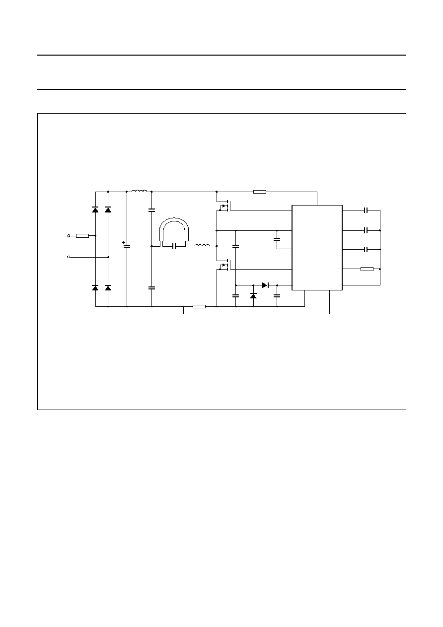
APPLICATION INFORMATION
handbook, full pagewidth
MGS994
30 k
490 k
CCI
CI
RHV
G1
S1
FS
G2
VS
CP
CF
lamp
RREF
SGND
PGND
RS
Cboot
100 nF
100 nF
CS9
CS4
C4
C3
CS7
C2
DS6
DS7
DS4
DS3
DS2
DS1
13
7
9
14
CCP
C5
100 nF
8
CCF
100 pF
12
RRREF
Rshunt
RRHV
Vin
10
T2
T1
11
2
3
1
6
5
UBA2021
R1
L1
L2
mains
supply
Fig.7 Application diagram.
2001 Jan 30
13
Philips Semiconductors
Product specification
630 V driver IC for CFL and TL lamps
UBA2021
PACKAGE OUTLINES
UNIT
A
max.
A
1
A
2
A
3
b
p
c
D
(1)
E
(1)
(1)
e
H
E
L
L
p
Q
Z
y
w
v
REFERENCES
OUTLINE
VERSION
EUROPEAN
PROJECTION
ISSUE DATE
IEC
JEDEC
EIAJ
mm
inches
1.75
0.25
0.10
1.45
1.25
0.25
0.49
0.36
0.25
0.19
8.75
8.55
4.0
3.8
1.27
6.2
5.8
0.7
0.6
0.7
0.3
8
0
o
o
0.25
0.1
DIMENSIONS (inch dimensions are derived from the original mm dimensions)
Note
1. Plastic or metal protrusions of 0.15 mm maximum per side are not included.
1.0
0.4
SOT108-1
X
w
M
A
A
1
A
2
b
p
D
H
E
L
p
Q
detail X
E
Z
e
c
L
v
M
A
(A )
3
A
7
8
1
14
y
076E06
MS-012
pin 1 index
0.069
0.010
0.004
0.057
0.049
0.01
0.019
0.014
0.0100
0.0075
0.35
0.34
0.16
0.15
0.050
1.05
0.041
0.244
0.228
0.028
0.024
0.028
0.012
0.01
0.25
0.01
0.004
0.039
0.016
97-05-22
99-12-27
0
2.5
5 mm
scale
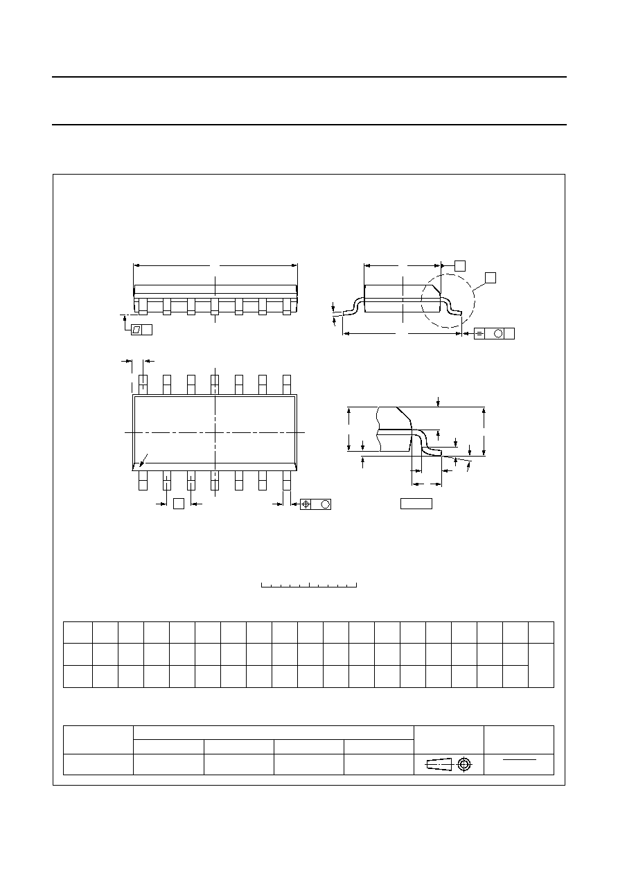
SO14: plastic small outline package; 14 leads; body width 3.9 mm
SOT108-1

2001 Jan 30
14
Philips Semiconductors
Product specification
630 V driver IC for CFL and TL lamps
UBA2021
UNIT
A
max.
1
2
(1)
(1)
b
1
c
D
(1)
Z
E
e
M
H
L
REFERENCES
OUTLINE
VERSION
EUROPEAN
PROJECTION
ISSUE DATE
IEC
JEDEC
EIAJ
mm
inches
DIMENSIONS (inch dimensions are derived from the original mm dimensions)
SOT27-1
95-03-11
99-12-27
A
min.
A
max.
b
max.
w
M
E
e
1
1.73
1.13
0.53
0.38
0.36
0.23
19.50
18.55
6.48
6.20
3.60
3.05
0.254
2.54
7.62
8.25
7.80
10.0
8.3
2.2
4.2
0.51
3.2
0.068
0.044
0.021
0.015
0.77
0.73
0.014
0.009
0.26
0.24
0.14
0.12
0.01
0.10
0.30
0.32
0.31
0.39
0.33
0.087
0.17
0.020
0.13
050G04
MO-001
SC-501-14
M
H
c
(e )
1
M
E
A
L
seating plane
A
1
w
M
b
1
e
D
A
2
Z
14
1
8
7
b
E
pin 1 index
0
5
10 mm
scale
Note
1. Plastic or metal protrusions of 0.25 mm maximum per side are not included.
DIP14: plastic dual in-line package; 14 leads (300 mil)
SOT27-1

2001 Jan 30
15
Philips Semiconductors
Product specification
630 V driver IC for CFL and TL lamps
UBA2021
SOLDERING
Introduction
This text gives a very brief insight to a complex technology.
A more in-depth account of soldering ICs can be found in
our
"Data Handbook IC26; Integrated Circuit Packages"
(document order number 9398 652 90011).
There is no soldering method that is ideal for all IC
packages. Wave soldering is often preferred when
through-hole and surface mount components are mixed on
one printed-circuit board. However, wave soldering is not
always suitable for surface mount ICs, or for printed-circuit
boards with high population densities. In these situations
reflow soldering is often used.
Through-hole mount packages
S
OLDERING BY DIPPING OR BY SOLDER WAVE
The maximum permissible temperature of the solder is
260
∞
C; solder at this temperature must not be in contact
with the joints for more than 5 seconds. The total contact
time of successive solder waves must not exceed
5 seconds.
The device may be mounted up to the seating plane, but
the temperature of the plastic body must not exceed the
specified maximum storage temperature (T
stg(max)
). If the
printed-circuit board has been pre-heated, forced cooling
may be necessary immediately after soldering to keep the
temperature within the permissible limit.
M
ANUAL SOLDERING
Apply the soldering iron (24 V or less) to the lead(s) of the
package, either below the seating plane or not more than
2 mm above it. If the temperature of the soldering iron bit
is less than 300
∞
C it may remain in contact for up to
10 seconds. If the bit temperature is between
300 and 400
∞
C, contact may be up to 5 seconds.
Surface mount packages
R
EFLOW SOLDERING
Reflow soldering requires solder paste (a suspension of
fine solder particles, flux and binding agent) to be applied
to the printed-circuit board by screen printing, stencilling or
pressure-syringe dispensing before package placement.
Several methods exist for reflowing; for example,
infrared/convection heating in a conveyor type oven.
Throughput times (preheating, soldering and cooling) vary
between 100 and 200 seconds depending on heating
method.
Typical reflow peak temperatures range from
215 to 250
∞
C. The top-surface temperature of the
packages should preferable be kept below 230
∞
C.
W
AVE SOLDERING
Conventional single wave soldering is not recommended
for surface mount devices (SMDs) or printed-circuit boards
with a high component density, as solder bridging and
non-wetting can present major problems.
To overcome these problems the double-wave soldering
method was specifically developed.
If wave soldering is used the following conditions must be
observed for optimal results:
∑
Use a double-wave soldering method comprising a
turbulent wave with high upward pressure followed by a
smooth laminar wave.
∑
For packages with leads on two sides and a pitch (e):
≠ larger than or equal to 1.27 mm, the footprint
longitudinal axis is preferred to be parallel to the
transport direction of the printed-circuit board;
≠ smaller than 1.27 mm, the footprint longitudinal axis
must be parallel to the transport direction of the
printed-circuit board.
The footprint must incorporate solder thieves at the
downstream end.
∑
For packages with leads on four sides, the footprint must
be placed at a 45
∞
angle to the transport direction of the
printed-circuit board. The footprint must incorporate
solder thieves downstream and at the side corners.
During placement and before soldering, the package must
be fixed with a droplet of adhesive. The adhesive can be
applied by screen printing, pin transfer or syringe
dispensing. The package can be soldered after the
adhesive is cured.
Typical dwell time is 4 seconds at 250
∞
C.
A mildly-activated flux will eliminate the need for removal
of corrosive residues in most applications.
M
ANUAL SOLDERING
Fix the component by first soldering two
diagonally-opposite end leads. Use a low voltage (24 V or
less) soldering iron applied to the flat part of the lead.
Contact time must be limited to 10 seconds at up to
300
∞
C.
When using a dedicated tool, all other leads can be
soldered in one operation within 2 to 5 seconds between
270 and 320
∞
C.

2001 Jan 30
16
Philips Semiconductors
Product specification
630 V driver IC for CFL and TL lamps
UBA2021
Suitability of IC packages for wave, reflow and dipping soldering methods
Notes
1. All surface mount (SMD) packages are moisture sensitive. Depending upon the moisture content, the maximum
temperature (with respect to time) and body size of the package, there is a risk that internal or external package
cracks may occur due to vaporization of the moisture in them (the so called popcorn effect). For details, refer to the
Drypack information in the
"Data Handbook IC26; Integrated Circuit Packages; Section: Packing Methods".
2. For SDIP packages, the longitudinal axis must be parallel to the transport direction of the printed-circuit board.
3. These packages are not suitable for wave soldering as a solder joint between the printed-circuit board and heatsink
(at bottom version) can not be achieved, and as solder may stick to the heatsink (on top version).
4. If wave soldering is considered, then the package must be placed at a 45
∞
angle to the solder wave direction.
The package footprint must incorporate solder thieves downstream and at the side corners.
5. Wave soldering is only suitable for LQFP, QFP and TQFP packages with a pitch (e) equal to or larger than 0.8 mm;
it is definitely not suitable for packages with a pitch (e) equal to or smaller than 0.65 mm.
6. Wave soldering is only suitable for SSOP and TSSOP packages with a pitch (e) equal to or larger than 0.65 mm; it is
definitely not suitable for packages with a pitch (e) equal to or smaller than 0.5 mm.
MOUNTING
PACKAGE
SOLDERING METHOD
WAVE
REFLOW
(1)
DIPPING
Through-hole mount DBS, DIP, HDIP, SDIP, SIL
suitable
(2)
-
suitable
Surface mount
BGA, LFBGA, SQFP, TFBGA
not suitable
suitable
-
HBCC, HLQFP, HSQFP, HSOP, HTQFP,
HTSSOP, SMS
not suitable
(3)
suitable
-
PLCC
(4)
, SO, SOJ
suitable
suitable
-
LQFP, QFP, TQFP
not recommended
(4)(5)
suitable
-
SSOP, TSSOP, VSO
not recommended
(6)
suitable
-

2001 Jan 30
17
Philips Semiconductors
Product specification
630 V driver IC for CFL and TL lamps
UBA2021
DATA SHEET STATUS
Note
1. Please consult the most recently issued data sheet before initiating or completing a design.
DATA SHEET STATUS
PRODUCT
STATUS
DEFINITIONS
(1)
Objective specification
Development
This data sheet contains the design target or goal specifications for
product development. Specification may change in any manner without
notice.
Preliminary specification
Qualification
This data sheet contains preliminary data, and supplementary data will be
published at a later date. Philips Semiconductors reserves the right to
make changes at any time without notice in order to improve design and
supply the best possible product.
Product specification
Production
This data sheet contains final specifications. Philips Semiconductors
reserves the right to make changes at any time without notice in order to
improve design and supply the best possible product.
DEFINITIONS
Short-form specification
The data in a short-form
specification is extracted from a full data sheet with the
same type number and title. For detailed information see
the relevant data sheet or data handbook.
Limiting values definition
Limiting values given are in
accordance with the Absolute Maximum Rating System
(IEC 60134). Stress above one or more of the limiting
values may cause permanent damage to the device.
These are stress ratings only and operation of the device
at these or at any other conditions above those given in the
Characteristics sections of the specification is not implied.
Exposure to limiting values for extended periods may
affect device reliability.
Application information
Applications that are
described herein for any of these products are for
illustrative purposes only. Philips Semiconductors make
no representation or warranty that such applications will be
suitable for the specified use without further testing or
modification.
DISCLAIMERS
Life support applications
These products are not
designed for use in life support appliances, devices, or
systems where malfunction of these products can
reasonably be expected to result in personal injury. Philips
Semiconductors customers using or selling these products
for use in such applications do so at their own risk and
agree to fully indemnify Philips Semiconductors for any
damages resulting from such application.
Right to make changes
Philips Semiconductors
reserves the right to make changes, without notice, in the
products, including circuits, standard cells, and/or
software, described or contained herein in order to
improve design and/or performance. Philips
Semiconductors assumes no responsibility or liability for
the use of any of these products, conveys no licence or title
under any patent, copyright, or mask work right to these
products, and makes no representations or warranties that
these products are free from patent, copyright, or mask
work right infringement, unless otherwise specified.

2001 Jan 30
18
Philips Semiconductors
Product specification
630 V driver IC for CFL and TL lamps
UBA2021
NOTES

2001 Jan 30
19
Philips Semiconductors
Product specification
630 V driver IC for CFL and TL lamps
UBA2021
NOTES

© Philips Electronics N.V.
SCA
All rights are reserved. Reproduction in whole or in part is prohibited without the prior written consent of the copyright owner.
The information presented in this document does not form part of any quotation or contract, is believed to be accurate and reliable and may be changed
without notice. No liability will be accepted by the publisher for any consequence of its use. Publication thereof does not convey nor imply any license
under patent- or other industrial or intellectual property rights.
Internet: http://www.semiconductors.philips.com
2001
71
Philips Semiconductors ≠ a worldwide company
For all other countries apply to: Philips Semiconductors,
Marketing Communications, Building BE-p, P.O. Box 218, 5600 MD EINDHOVEN,
The Netherlands, Fax. +31 40 27 24825
Argentina: see South America
Australia: 3 Figtree Drive, HOMEBUSH, NSW 2140,
Tel. +61 2 9704 8141, Fax. +61 2 9704 8139
Austria: Computerstr. 6, A-1101 WIEN, P.O. Box 213,
Tel. +43 1 60 101 1248, Fax. +43 1 60 101 1210
Belarus: Hotel Minsk Business Center, Bld. 3, r. 1211, Volodarski Str. 6,
220050 MINSK, Tel. +375 172 20 0733, Fax. +375 172 20 0773
Belgium: see The Netherlands
Brazil: see South America
Bulgaria: Philips Bulgaria Ltd., Energoproject, 15th floor,
51 James Bourchier Blvd., 1407 SOFIA,
Tel. +359 2 68 9211, Fax. +359 2 68 9102
Canada: PHILIPS SEMICONDUCTORS/COMPONENTS,
Tel. +1 800 234 7381, Fax. +1 800 943 0087
China/Hong Kong: 501 Hong Kong Industrial Technology Centre,
72 Tat Chee Avenue, Kowloon Tong, HONG KONG,
Tel. +852 2319 7888, Fax. +852 2319 7700
Colombia: see South America
Czech Republic: see Austria
Denmark: Sydhavnsgade 23, 1780 COPENHAGEN V,
Tel. +45 33 29 3333, Fax. +45 33 29 3905
Finland: Sinikalliontie 3, FIN-02630 ESPOO,
Tel. +358 9 615 800, Fax. +358 9 6158 0920
France: 51 Rue Carnot, BP317, 92156 SURESNES Cedex,
Tel. +33 1 4099 6161, Fax. +33 1 4099 6427
Germany: Hammerbrookstraþe 69, D-20097 HAMBURG,
Tel. +49 40 2353 60, Fax. +49 40 2353 6300
Hungary: Philips Hungary Ltd., H-1119 Budapest, Fehervari ut 84/A,
Tel: +36 1 382 1700, Fax: +36 1 382 1800
India: Philips INDIA Ltd, Band Box Building, 2nd floor,
254-D, Dr. Annie Besant Road, Worli, MUMBAI 400 025,
Tel. +91 22 493 8541, Fax. +91 22 493 0966
Indonesia: PT Philips Development Corporation, Semiconductors Division,
Gedung Philips, Jl. Buncit Raya Kav.99-100, JAKARTA 12510,
Tel. +62 21 794 0040 ext. 2501, Fax. +62 21 794 0080
Ireland: Newstead, Clonskeagh, DUBLIN 14,
Tel. +353 1 7640 000, Fax. +353 1 7640 200
Israel: RAPAC Electronics, 7 Kehilat Saloniki St, PO Box 18053,
TEL AVIV 61180, Tel. +972 3 645 0444, Fax. +972 3 649 1007
Italy: PHILIPS SEMICONDUCTORS, Via Casati, 23 - 20052 MONZA (MI),
Tel. +39 039 203 6838, Fax +39 039 203 6800
Japan: Philips Bldg 13-37, Kohnan 2-chome, Minato-ku,
TOKYO 108-8507, Tel. +81 3 3740 5130, Fax. +81 3 3740 5057
Korea: Philips House, 260-199 Itaewon-dong, Yongsan-ku, SEOUL,
Tel. +82 2 709 1412, Fax. +82 2 709 1415
Malaysia: No. 76 Jalan Universiti, 46200 PETALING JAYA, SELANGOR,
Tel. +60 3 750 5214, Fax. +60 3 757 4880
Mexico: 5900 Gateway East, Suite 200, EL PASO, TEXAS 79905,
Tel. +9-5 800 234 7381, Fax +9-5 800 943 0087
Middle East: see Italy
Netherlands: Postbus 90050, 5600 PB EINDHOVEN, Bldg. VB,
Tel. +31 40 27 82785, Fax. +31 40 27 88399
New Zealand: 2 Wagener Place, C.P.O. Box 1041, AUCKLAND,
Tel. +64 9 849 4160, Fax. +64 9 849 7811
Norway: Box 1, Manglerud 0612, OSLO,
Tel. +47 22 74 8000, Fax. +47 22 74 8341
Pakistan: see Singapore
Philippines: Philips Semiconductors Philippines Inc.,
106 Valero St. Salcedo Village, P.O. Box 2108 MCC, MAKATI,
Metro MANILA, Tel. +63 2 816 6380, Fax. +63 2 817 3474
Poland: Al.Jerozolimskie 195 B, 02-222 WARSAW,
Tel. +48 22 5710 000, Fax. +48 22 5710 001
Portugal: see Spain
Romania: see Italy
Russia: Philips Russia, Ul. Usatcheva 35A, 119048 MOSCOW,
Tel. +7 095 755 6918, Fax. +7 095 755 6919
Singapore: Lorong 1, Toa Payoh, SINGAPORE 319762,
Tel. +65 350 2538, Fax. +65 251 6500
Slovakia: see Austria
Slovenia: see Italy
South Africa: S.A. PHILIPS Pty Ltd., 195-215 Main Road Martindale,
2092 JOHANNESBURG, P.O. Box 58088 Newville 2114,
Tel. +27 11 471 5401, Fax. +27 11 471 5398
South America: Al. Vicente Pinzon, 173, 6th floor,
04547-130 S√O PAULO, SP, Brazil,
Tel. +55 11 821 2333, Fax. +55 11 821 2382
Spain: Balmes 22, 08007 BARCELONA,
Tel. +34 93 301 6312, Fax. +34 93 301 4107
Sweden: Kottbygatan 7, Akalla, S-16485 STOCKHOLM,
Tel. +46 8 5985 2000, Fax. +46 8 5985 2745
Switzerland: Allmendstrasse 140, CH-8027 ZÐRICH,
Tel. +41 1 488 2741 Fax. +41 1 488 3263
Taiwan: Philips Semiconductors, 5F, No. 96, Chien Kuo N. Rd., Sec. 1,
TAIPEI, Taiwan Tel. +886 2 2134 2451, Fax. +886 2 2134 2874
Thailand: PHILIPS ELECTRONICS (THAILAND) Ltd.,
60/14 MOO 11, Bangna Trad Road KM. 3, Bagna, BANGKOK 10260,
Tel. +66 2 361 7910, Fax. +66 2 398 3447
Turkey: Yukari Dudullu, Org. San. Blg., 2.Cad. Nr. 28 81260 Umraniye,
ISTANBUL, Tel. +90 216 522 1500, Fax. +90 216 522 1813
Ukraine: PHILIPS UKRAINE, 4 Patrice Lumumba str., Building B, Floor 7,
252042 KIEV, Tel. +380 44 264 2776, Fax. +380 44 268 0461
United Kingdom: Philips Semiconductors Ltd., 276 Bath Road, Hayes,
MIDDLESEX UB3 5BX, Tel. +44 208 730 5000, Fax. +44 208 754 8421
United States: 811 East Arques Avenue, SUNNYVALE, CA 94088-3409,
Tel. +1 800 234 7381, Fax. +1 800 943 0087
Uruguay: see South America
Vietnam: see Singapore
Yugoslavia: PHILIPS, Trg N. Pasica 5/v, 11000 BEOGRAD,
Tel. +381 11 3341 299, Fax.+381 11 3342 553
Printed in The Netherlands
613502/02/pp
20
Date of release:
2001 Jan 30
Document order number:
9397 750 07752