 | –≠–ª–µ–∫—Ç—Ä–æ–Ω–Ω—ã–π –∫–æ–º–ø–æ–Ω–µ–Ω—Ç: UBA2024 | –°–∫–∞—á–∞—Ç—å:  PDF PDF  ZIP ZIP |

DATA SHEET
Product specification
Supersedes data of 2003 Aug 13
2004 Feb 03
INTEGRATED CIRCUITS
UBA2024
Half-bridge power IC for CFL lamps

2004 Feb 03
2
Philips Semiconductors
Product specification
Half-bridge power IC for CFL lamps
UBA2024
FEATURES
∑
Integrated half-bridge power transistors
∑
Integrated bootstrap diode
∑
Integrated low-voltage supply
∑
Maximum voltage of 550 V
∑
Adjustable oscillator frequency
∑
Soft start
∑
Minimum glow time control.
APPLICATIONS
∑
Driver for any kind of load in a half-bridge configuration
∑
Especially for electronically self-ballasted Compact
Fluorescent Lamps (CFL) for lamp currents up to
220 mA (RMS) under the restriction that the maximum
junction temperature is not exceeded.
GENERAL DESCRIPTION
The UBA2024 is a high-voltage monolithic integrated
circuit made in the EZ-HV SOI process. The IC is designed
for driving CFL lamps in a half-bridge configuration.
The IC features a soft start function, an adjustable internal
oscillator and an internal drive function with a high-voltage
level shifter for driving the half-bridge.
To guarantee an accurate 50% duty cycle, the oscillator
signal is passed through a divider before being fed to the
output drivers.
ORDERING INFORMATION
BLOCK DIAGRAM
TYPE
NUMBER
PACKAGE
NAME
DESCRIPTION
VERSION
UBA2024P
DIP8
plastic dual in-line package; 8 leads (300 mil)
SOT97-1
mdb029
SWEEP AND
GLOW TIME CONTROL
HIGH VOLTAGE
LEVEL SHIFTER
V
DD
CONTROL
HIGH SIDE
DRIVER
LOW SIDE
DRIVER
OSCILLATOR
DIVIDE-BY-2
DEAD TIME
UBA2024
2
8
V
DD
V
DD(stop)
SW
RC
SGND
1
7
6
HV
FS
HS
LS
OUT
PGND
3
5
4
Fig.1 Block diagram.

2004 Feb 03
3
Philips Semiconductors
Product specification
Half-bridge power IC for CFL lamps
UBA2024
PINNING
SYMBOL
PIN
DESCRIPTION
SW
1
sweep timing input
SGND
2
signal ground
FS
3
high-side floating supply output
PGND
4
power ground
OUT
5
half-bridge output
HV
6
high-voltage supply
V
DD
7
internal low-voltage supply
output
RC
8
internal oscillator input
handbook, halfpage
1
2
3
4
8
7
6
5
MCE409
UBA2024P
RC
VDD
SGND
HV
OUT
PGND
FS
SW
Fig.2 Pin configuration DIP8 package.
FUNCTIONAL DESCRIPTION
Supply voltage
The UBA2024 is powered by a supply voltage applied to
pin HV. The IC generates its own low supply voltage for
the internal circuitry and therefore, an additional external
low-voltage supply is not required.
Start-up state
With an increase of the supply voltage on pin HV, the IC
enters the start-up state. In the start-up state the high-side
power transistor is not conducting and the low-side power
transistor is switched on. The internal circuit is reset and
the capacitors on the bootstrap pin FS and low-voltage
supply pin V
DD
are charged. Pins RC and SW are
switched to ground. The start-up state is defined until
V
DD
= V
DD(start)
.
Sweep mode
The IC enters the sweep mode at the moment the voltage
on pin V
DD
> V
DD(start)
. The capacitor on pin SW is charged
by I
sweep
and the half-bridge circuit starts oscillating. The
circuit enters the start-up state again when the voltage on
pin V
DD
< V
DD(stop)
.
Reset
A DC reset circuit is incorporated in the high-side driver.
The high-side transistor is switched off when the voltage
on pin FS is below the high-side lockout voltage V
FS(lock)
.
Oscillation
The oscillation is based upon the 555-timer function. With
the external resistor R
OSC
and capacitor C
OSC
(see Fig.5)
a self oscillating circuit is made, where R
OSC
and C
OSC
determine the oscillating frequency.
To realize an accurate 50% duty cycle, an internal divider
is used. Due to the presence of the divider, the bridge
frequency is half the oscillator frequency.
The output voltage of the bridge will change at the falling
edge of the signal on pin RC. The design equation for the
half-bridge frequency is:
An overview of the oscillator signal, internal LS and HS
drive signals and the output is given in Fig.3.
f
osc
1
k
R
OSC
C
OSC
◊
◊
---------------------------------------------
=

2004 Feb 03
4
Philips Semiconductors
Product specification
Half-bridge power IC for CFL lamps
UBA2024
When entering the sweep mode, the oscillator starts at
2.5 times the nominal bridge frequency and sweeps down
to the nominal bridge frequency f
nom
; see Fig.4. During this
continuously decreasing of the frequency, the circuit
approaches the resonance frequency of the load. This
causes a high voltage across the load, which normally
ignites the lamp.
The sweep time t
sweep
is determined by the charge current
I
ch(sw)
and the external capacitor C
SW
. The sweep to
resonance time should be much larger than the settling
time of the supply voltage on pin HV to guarantee that the
full high-voltage is present at the moment of ignition.
The amplitude of the RC oscillator is equal to the minimum
value of V
RC(h)
and V
SW
+ 0.4
◊
V
RC(h)
.
During the sweep time a current is flowing through the
lamp electrodes for pre-heating the filaments.
Glow time control
The drawback of cold-started CFL lamps is its inherent
glow time which reduces the switching lifetime of the
electrodes (lamp). To make this glow phase as short as
possible, the maximum power is given to the lamp during
the glow time via a special control; see Fig.4.
Non-overlap time
The non-overlap time is defined as the time that both
MOSFETs are not conducting. The non-overlap time is
internally fixed.
handbook, halfpage
MDB031
VRC
VOUT
HS
drive
LS
drive
time
time
time
time
half
bridge
0
0
0
0
Fig.3 Oscillator, drivers and output signals.
handbook, halfpage
VHV
VDD
VDD
0.8VRC(h)
VSW
fosc
Vlamp
Vign
Vglow
Vnom
2.5fnom
fnom
VDD(start)
0
0
0
0
MDB032
time
time
time
time
time
minimum glow time control
tsweep
Fig.4 Start-up frequency behaviour.

2004 Feb 03
5
Philips Semiconductors
Product specification
Half-bridge power IC for CFL lamps
UBA2024
LIMITING VALUES
In accordance with the Absolute Maximum Rating System (IEC 60134); all voltages are measured with respect to
SGND; positive currents flow into the IC.
Notes
1. In accordance with the Human Body Model (HBM): equivalent to discharging a 100 pF capacitor through a 1.5 k
series resistor.
2. In accordance with the Machine Model (MM): equivalent to discharging a 200 pF capacitor through a 1.5 k
series
resistor and a 0.75
µ
H inductor.
QUALITY SPECIFICATION
Quality in accordance with
SNW-FQ-611.
THERMAL CHARACTERISTICS
Note
1. In accordance with IEC 60747-1.
SYMBOL
PARAMETER
CONDITIONS
MIN.
MAX.
UNIT
V
HV
high-voltage supply voltage
normal operation
-
373
V
mains transients
during 0.5 s
-
550
V
V
FS
floating supply voltage
V
HV
V
HV
+ 14
V
V
DD
low-voltage output supply voltage
DC supply
0
14
V
I
DD
low-voltage output supply current
peak value is internally
limited; T
amb
= 25
∞
C
0
5
mA
V
PGND
power ground voltage
referenced to SGND
-
1
+1
V
V
i(RC)
internal oscillator input voltage on pin RC
I
i(RC)
< 1 mA
0
V
DD
V
V
i(SW)
sweep time input voltage on pin SW
I
i(SW)
< 1 mA
0
V
DD
V
SR
slew rate output on pin OUT
repetitive
-
4
+4
V/ns
T
j
junction temperature
-
40
+150
∞
C
T
amb
ambient temperature
-
40
+150
∞
C
T
stg
storage temperature
-
55
+150
∞
C
V
esd(HBM)
HBM electrostatic discharge voltage on pins
note 1
HV and V
DD
-
1000
V
SW, RC, FS and OUT
-
2500
V
V
esd(MM)
MM electrostatic discharge voltage on pins
note 2
FS
-
200
V
HV, V
DD
, SW, RC and OUT
-
250
V
SYMBOL
PARAMETER
CONDITIONS
TYP.
UNIT
R
th(j-a)
thermal resistance from junction to ambient
in free air; note 1
95
K/W
R
th(j-c)
thermal resistance from junction to case
note 1
16
K/W

2004 Feb 03
6
Philips Semiconductors
Product specification
Half-bridge power IC for CFL lamps
UBA2024
CHARACTERISTICS
T
j
= 25
∞
C; all voltages are measured with respect to SGND; positive currents flow into the IC.
SYMBOL
PARAMETER
CONDITIONS
MIN.
TYP.
MAX.
UNIT
High-voltage supply
V
HV
high-voltage supply voltage
t < 0.5 s and I
HV
< 30
µ
A
0
-
550
V
V
FS
floating supply voltage
t < 0.5 s and I
FS
< 30
µ
A
0
-
564
V
Low-voltage supply
V
DD
low-voltage output supply voltage
V
HV
= 100 V; R
OSC
=
;
V
SW
= V
DD
; V
RC
= 0 V
11.7
12.5
13.3
V
Start-up state
I
HV
high-voltage supply current
V
HV
= 100 V; R
OSC
=
;
V
SW
= V
DD
; V
RC
= 0 V
-
-
0.39
mA
V
DD(start)
start of oscillation voltage
10
11
12
V
V
DD(stop)
stop of oscillation voltage
8
8.5
9
V
V
DD(hys)
start-stop hysteresis voltage
2
2.5
3
V
Output stage
R
HS(on)
HS transistor on-resistance
V
HV
= 310 V; I
d
= 100 mA
-
9.7
11
R
LS(on)
LS transistor on-resistance
I
d
= 100 mA
-
8.5
9.4
V
HS(d)
HS body diode forward voltage
I
f
= 200 mA
1.4
1.8
2.2
V
V
LS(d)
LS body diode forward voltage
I
f
= 200 mA
1.2
1.6
2.0
V
I
HS(sat)
HS transistor saturation current
V
ds
= 30 V; T
j
125
∞
C;
V
HV
= 310 V
900
-
-
mA
I
LS(sat)
LS transistor saturation current
V
ds
= 30 V; T
j
125
∞
C
900
-
-
mA
V
boot
bootstrap diode drop voltage
I
f
= 1 mA
0.7
1.0
1.3
V
t
no
non overlap time
1
1.35
1.7
µ
s
V
FS(lock)
floating supply lock-out voltage
3.6
4.2
4.8
V
I
FS
floating supply current
V
HV
= 310 V; V
FS
= 12.2 V
10
14
18
µ
A
Internal oscillator
f
osc
frequency range bridge oscillator
V
SW
= V
DD
-
-
60
kHz
f
osc(nom)
nominal frequency bridge oscillator
R
OSC
= 100 k
; C
OSC
= 220 pF;
V
SW
= V
DD
40.05
41.32
42.68
kHz
f
osc(nom)
bridge oscillator frequency variation
with temperature
R
OSC
= 100 k
; C
OSC
= 220 pF;
T =
-
20 to +150
∞
C
-
2
-
%
k
h
high-level trip point factor
0.382
0.395
0.408
V
RC(h)
high-level trip point voltage on
pin RC
V
RC(h)
= k
h
◊
V
DD
4.58
4.94
5.29
V
k
l
low-level trip point factor
0.030
0.033
0.036
V
RC(low)
low-level trip point voltage on
pin RC
V
RC(l)
= k
l
◊
V
DD
0.367
0.413
0.458
V
k
osc
oscillator constant
R
OSC
= 100 k
; C
OSC
= 220 pF
1.065
1.1
1.135

2004 Feb 03
7
Philips Semiconductors
Product specification
Half-bridge power IC for CFL lamps
UBA2024
APPLICATION INFORMATION
Sweep function
I
ch(sw)
charge current for sweep
V
SW
= 0 V
215
280
345
nA
t
sweep
sweep time
C
SW
= 33 nF; V
DD
= 12.2 V
0.28
0.35
0.45
s
SYMBOL
PARAMETER
CONDITIONS
MIN.
TYP.
MAX.
UNIT
mdb033
CBUF
4.7 uF
LFILT
1.8 mH
RFUS
33
D1
D3
D2
D4
CHB2
47 nF
11 W/150 mA
max. 550 V
3.1 mH
LLA
CHB1
47 nF
ROSC
110 K
COSC
180 pF
CFS
10 nF
CDV
100 pF
CVDD
10 nF
CLA
1.5 nF
5
6
4
3
8
1
2
7
UBA2024P
SW
V
DD
RC
SGND
HV
FS
OUT
PGND
CSW
33 nF
AC mains
supply
(230 V)
Fig.5 Typical integrated CFL application with UBA2024P at f = 46 kHz.

2004 Feb 03
8
Philips Semiconductors
Product specification
Half-bridge power IC for CFL lamps
UBA2024
PACKAGE OUTLINES
REFERENCES
OUTLINE
VERSION
EUROPEAN
PROJECTION
ISSUE DATE
IEC
JEDEC
JEITA
SOT97-1
99-12-27
03-02-13
UNIT
A
max.
1
2
b
1
(1)
(1)
(1)
b
2
c
D
E
e
M
Z
H
L
mm
DIMENSIONS (inch dimensions are derived from the original mm dimensions)
A
min.
A
max.
b
max.
w
M
E
e
1
1.73
1.14
0.53
0.38
0.36
0.23
9.8
9.2
6.48
6.20
3.60
3.05
0.254
2.54
7.62
8.25
7.80
10.0
8.3
1.15
4.2
0.51
3.2
inches
0.068
0.045
0.021
0.015
0.014
0.009
1.07
0.89
0.042
0.035
0.39
0.36
0.26
0.24
0.14
0.12
0.01
0.1
0.3
0.32
0.31
0.39
0.33
0.045
0.17
0.02
0.13
b
2
050G01
MO-001
SC-504-8
M
H
c
(e )
1
M
E
A
L
seating plane
A
1
w
M
b
1
e
D
A
2
Z
8
1
5
4
b
E
0
5
10 mm
scale
Note
1. Plastic or metal protrusions of 0.25 mm (0.01 inch) maximum per side are not included.
pin 1 index
DIP8: plastic dual in-line package; 8 leads (300 mil)
SOT97-1
2004 Feb 03
9
Philips Semiconductors
Product specification
Half-bridge power IC for CFL lamps
UBA2024
SOLDERING
Introduction to soldering through-hole mount
packages
This text gives a brief insight to wave, dip and manual
soldering. A more in-depth account of soldering ICs can be
found in our
"Data Handbook IC26; Integrated Circuit
Packages" (document order number 9398 652 90011).
Wave soldering is the preferred method for mounting of
through-hole mount IC packages on a printed-circuit
board.
Soldering by dipping or by solder wave
Driven by legislation and environmental forces the
worldwide use of lead-free solder pastes is increasing.
Typical dwell time of the leads in the wave ranges from
3 to 4 seconds at 250
∞
C or 265
∞
C, depending on solder
material applied, SnPb or Pb-free respectively.
The total contact time of successive solder waves must not
exceed 5 seconds.
The device may be mounted up to the seating plane, but
the temperature of the plastic body must not exceed the
specified maximum storage temperature (T
stg(max)
). If the
printed-circuit board has been pre-heated, forced cooling
may be necessary immediately after soldering to keep the
temperature within the permissible limit.
Manual soldering
Apply the soldering iron (24 V or less) to the lead(s) of the
package, either below the seating plane or not more than
2 mm above it. If the temperature of the soldering iron bit
is less than 300
∞
C it may remain in contact for up to
10 seconds. If the bit temperature is between
300 and 400
∞
C, contact may be up to 5 seconds.
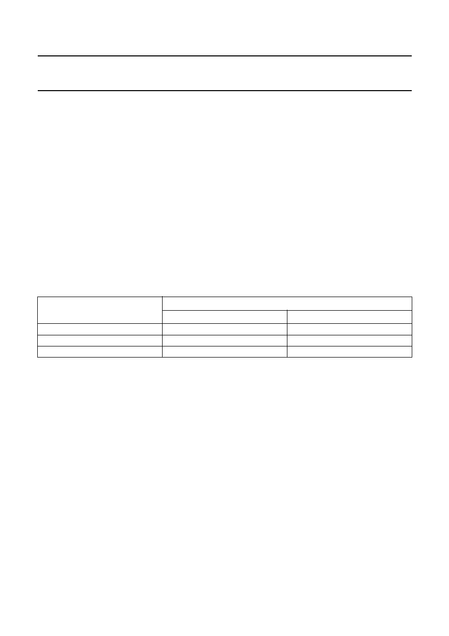
Suitability of through-hole mount IC packages for dipping and wave soldering methods
Notes
1. For SDIP packages, the longitudinal axis must be parallel to the transport direction of the printed-circuit board.
2. For PMFP packages hot bar soldering or manual soldering is suitable.
PACKAGE
SOLDERING METHOD
DIPPING
WAVE
CPGA, HCPGA
-
suitable
DBS, DIP, HDIP, RDBS, SDIP, SIL
suitable
suitable
(1)
PMFP
(2)
-
not suitable

2004 Feb 03
10
Philips Semiconductors
Product specification
Half-bridge power IC for CFL lamps
UBA2024
DATA SHEET STATUS
Notes
1. Please consult the most recently issued data sheet before initiating or completing a design.
2. The product status of the device(s) described in this data sheet may have changed since this data sheet was
published. The latest information is available on the Internet at URL http://www.semiconductors.philips.com.
3. For data sheets describing multiple type numbers, the highest-level product status determines the data sheet status.
LEVEL
DATA SHEET
STATUS
(1)
PRODUCT
STATUS
(2)(3)
DEFINITION
I
Objective data
Development
This data sheet contains data from the objective specification for product
development. Philips Semiconductors reserves the right to change the
specification in any manner without notice.
II
Preliminary data Qualification
This data sheet contains data from the preliminary specification.
Supplementary data will be published at a later date. Philips
Semiconductors reserves the right to change the specification without
notice, in order to improve the design and supply the best possible
product.
III
Product data
Production
This data sheet contains data from the product specification. Philips
Semiconductors reserves the right to make changes at any time in order
to improve the design, manufacturing and supply. Relevant changes will
be communicated via a Customer Product/Process Change Notification
(CPCN).
DEFINITIONS
Short-form specification
The data in a short-form
specification is extracted from a full data sheet with the
same type number and title. For detailed information see
the relevant data sheet or data handbook.
Limiting values definition
Limiting values given are in
accordance with the Absolute Maximum Rating System
(IEC 60134). Stress above one or more of the limiting
values may cause permanent damage to the device.
These are stress ratings only and operation of the device
at these or at any other conditions above those given in the
Characteristics sections of the specification is not implied.
Exposure to limiting values for extended periods may
affect device reliability.
Application information
Applications that are
described herein for any of these products are for
illustrative purposes only. Philips Semiconductors make
no representation or warranty that such applications will be
suitable for the specified use without further testing or
modification.
DISCLAIMERS
Life support applications
These products are not
designed for use in life support appliances, devices, or
systems where malfunction of these products can
reasonably be expected to result in personal injury. Philips
Semiconductors customers using or selling these products
for use in such applications do so at their own risk and
agree to fully indemnify Philips Semiconductors for any
damages resulting from such application.
Right to make changes
Philips Semiconductors
reserves the right to make changes in the products -
including circuits, standard cells, and/or software -
described or contained herein in order to improve design
and/or performance. When the product is in full production
(status `Production'), relevant changes will be
communicated via a Customer Product/Process Change
Notification (CPCN). Philips Semiconductors assumes no
responsibility or liability for the use of any of these
products, conveys no licence or title under any patent,
copyright, or mask work right to these products, and
makes no representations or warranties that these
products are free from patent, copyright, or mask work
right infringement, unless otherwise specified.

© Koninklijke Philips Electronics N.V. 2004
SCA76
All rights are reserved. Reproduction in whole or in part is prohibited without the prior written consent of the copyright owner.
The information presented in this document does not form part of any quotation or contract, is believed to be accurate and reliable and may be changed
without notice. No liability will be accepted by the publisher for any consequence of its use. Publication thereof does not convey nor imply any license
under patent- or other industrial or intellectual property rights.
Philips Semiconductors ≠ a worldwide company
Contact information
For additional information please visit http://www.semiconductors.philips.com.
Fax: +31 40 27 24825
For sales offices addresses send e-mail to: sales.addresses@www.semiconductors.philips.com.
Printed in The Netherlands
R79/02/pp
11
Date of release:
2004 Feb 03
Document order number:
9397 750 12676