Document Outline
- FEATURES
- GENERAL DESCRIPTION
- APPLICATIONS
- ORDERING INFORMATION
- QUICK REFERENCE DATA
- BLOCK DIAGRAM
- PINNING
- FUNCTIONAL DESCRIPTION
- LIMITING VALUES
- THERMAL CHARACTERISTICS
- QUALITY SPECIFICATION
- CHARACTERISTICS
- APPLICATION INFORMATION
- PACKAGE OUTLINE
- SOLDERING
- DATA SHEET STATUS
- DEFINITIONS
- DISCLAIMERS

DATA SHEET
Product specification
Supersedes data of 1999 Aug 10
2002 Sep 27
INTEGRATED CIRCUITS
UBA2030T
Full bridge driver IC

2002 Sep 27
2
Philips Semiconductors
Product specification
Full bridge driver IC
UBA2030T
FEATURES
∑
Full bridge driver
∑
Integrated bootstrap diodes
∑
Integrated high voltage level shift function
∑
High voltage input (570 V maximum) for the internal
supply
∑
Adjustable `dead time'
∑
Adjustable oscillator frequency
∑
High voltage level shifter for the bridge enable function
∑
Shut-down function.
APPLICATIONS
∑
The UBA2030T can drive the MOSFETs in any type of
load configured as a full bridge
∑
The circuit is intended as a commutator for High
Intensity Discharge (HID) lamps.
GENERAL DESCRIPTION
The UBA2030T is a high voltage integrated circuit
fabricated using the BCD750 power logic process. The
circuit is designed for driving the MOSFETs in a full bridge
configuration. In addition, it features a shut-down function,
an adjustable oscillator and a PMOS high voltage level
shifter to control the bridge enable function. To guarantee
an accurate 50% duty factor, the oscillator signal passes
through a divider before being fed to the output drivers.
ORDERING INFORMATION
TYPE NUMBER
PACKAGE
NAME
DESCRIPTION
VERSION
UBA2030T
SO24
plastic small outline package; 24 leads; body width 7.5 mm
SOT137-1

2002 Sep 27
3
Philips Semiconductors
Product specification
Full bridge driver IC
UBA2030T
QUICK REFERENCE DATA
SYMBOL
PARAMETER
CONDITIONS
MIN.
TYP.
MAX.
UNIT
High voltage
V
HV
high voltage supply
0
-
570
V
Start-up; powered via pin HV
I
strtu
start-up current
-
0.7
1.0
mA
V
th(oscstrt)
start oscillating threshold
voltage
at f
bridge
= 500 Hz; no load
14.0
15.5
17.0
V
V
th(oscstp)
stop oscillating threshold
voltage
11.5
13.0
14.5
V
Output drivers
I
o(source)
output source current
V
DD
= V
FSL
= V
FSR
= 15 V;
V
GHR
= V
GHL
= V
GLR
= V
GLL
= 0 V
140
190
240
mA
I
o(sink)
output sink current
V
DD
= V
FSL
= V
FSR
= 15 V;
V
GHR
= V
GHL
= V
GLR
= V
GLL
= 15 V
200
260
320
mA
Internal oscillator
f
bridge
bridge oscillating frequency
EXO pin connected to SGND
50
-
50000
Hz
External oscillator
f
osc(ext)
external oscillator frequency
RC pin connected to SGND;
100
-
100000 Hz
Dead time control
t
dead
dead time control range
adjusted externally
0.4
-
4
µ
s
Bridge enable
I
IH
HIGH-level input current
bridge enable active
100
-
700
µ
A
I
IL
LOW-level input current
bridge enable not active
0
-
20
µ
A
Shut-down
V
IH
HIGH-level input voltage
shut-down active;
4.5
-
V
DD
V
V
IL
LOW-level input voltage
shut-down not active;
0
-
0.5
V
f
bridge
f
osc(ext)
2
-----------------
=
V
SD
t
--------------
5 V/ms
>
V
SD
t
--------------
5 V/ms
>
2002 Sep 27
4
Philips Semiconductors
Product specification
Full bridge driver IC
UBA2030T
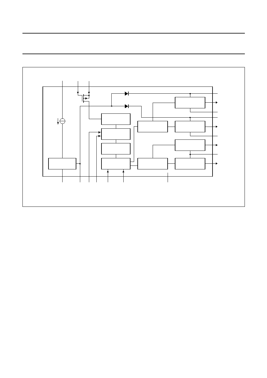
BLOCK DIAGRAM
Fig.1 Block diagram.
handbook, full pagewidth
MGK590
LOW VOLTAGE
LEVEL SHIFTER
LOW VOLTAGE
SUPPLY
HIGH VOLTAGE
LEVEL SHIFTER
HIGHER LEFT
DRIVER
LOWER LEFT
DRIVER
LOWER RIGHT
DRIVER
HIGHER RIGHT
DRIVER
BRIDGE ENABLE
OSCILLATOR
LOGIC
˜
2
18
24
23
5
20
22
8
7
HV
BER
BE
SGND
VDD RC EXO
DTC
21
SD
4, 6, 9, 16, 17, 19
n.c.
1
GLR
2
PGND
3
GLL
13
SHR
14
GHR
11
GHL
15
FSR
12
SHL
10
FSL
UBA2030T
2002 Sep 27
5
Philips Semiconductors
Product specification
Full bridge driver IC
UBA2030T
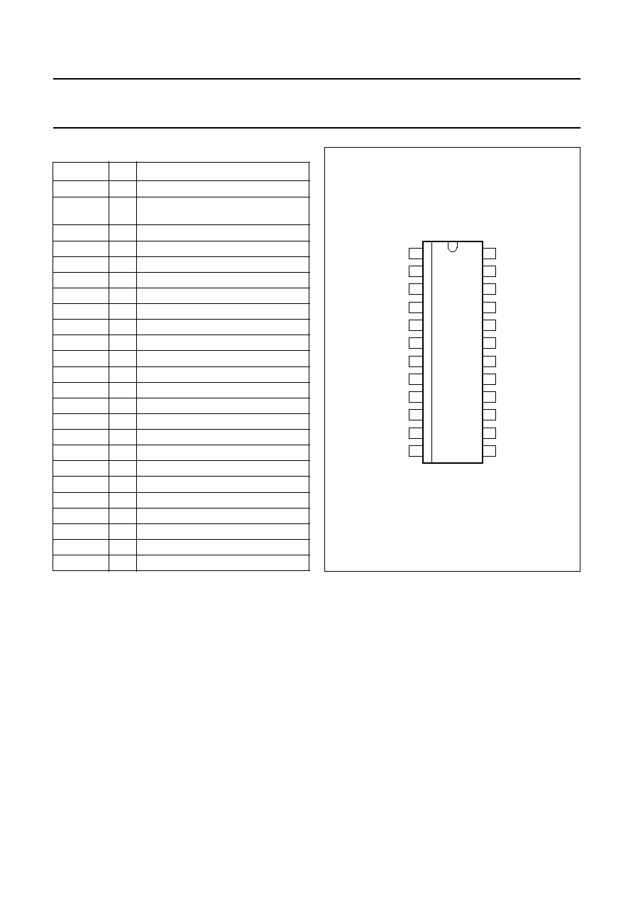
PINNING
SYMBOL
PIN
DESCRIPTION
GLR
1
gate of lower right MOSFET
PGND
2
power ground for sources of lower
left and right MOSFETs
GLL
3
gate of lower left MOSFET
n.c.
4
not connected
RC
5
RC input for internal oscillator
n.c.
6
not connected
BE
7
bridge enable control input
BER
8
bridge enable reference input
n.c.
9
not connected
FSL
10
floating supply voltage left side
GHL
11
gate of higher left MOSFET
SHL
12
source of higher left MOSFET
SHR
13
source of higher right MOSFET
GHR
14
gate of higher right MOSFET
FSR
15
floating supply voltage right side
n.c.
16
not connected
n.c.
17
not connected
HV
18
high voltage supply
n.c.
19
not connected
EXO
20
external oscillator input
SD
21
shut-down input
DTC
22
`dead time' control input
V
DD
23
internal (low voltage) supply
SGND
24
signal ground
Fig.2 Pin configuration.
handbook, halfpage
UBA2030T
GLR
PGND
GLL
n.c.
RC
n.c.
BE
BER
n.c.
FSL
GHL
SHL
SGND
VDD
DTC
SD
n.c.
HV
EXO
n.c.
n.c.
FSR
GHR
SHR
MGK589
1
2
3
4
5
6
7
8
9
10
11
12
24
23
22
21
20
19
18
17
16
15
14
13