 | –≠–ª–µ–∫—Ç—Ä–æ–Ω–Ω—ã–π –∫–æ–º–ø–æ–Ω–µ–Ω—Ç: UBA2033TS | –°–∫–∞—á–∞—Ç—å:  PDF PDF  ZIP ZIP |
Document Outline
- FEATURES
- APPLICATIONS
- GENERAL DESCRIPTION
- ORDERING INFORMATION
- BLOCK DIAGRAM
- PINNING
- FUNCTIONAL DESCRIPTION
- LIMITING VALUES
- THERMAL CHARACTERISTICS
- QUALITY SPECIFICATION
- CHARACTERISTICS
- APPLICATION INFORMATION
- PACKAGE OUTLINE
- SOLDERING
- DATA SHEET STATUS
- DEFINITIONS
- DISCLAIMERS

DATA SHEET
Product specification
2002 Oct 08
INTEGRATED CIRCUITS
UBA2033
HF full bridge driver IC

2002 Oct 08
2
Philips Semiconductors
Product specification
HF full bridge driver IC
UBA2033
FEATURES
∑
Full bridge driver circuit
∑
Integrated bootstrap diodes
∑
Integrated high voltage level shift function
∑
High voltage input for the internal supply voltage
∑
550 V maximum voltage
∑
Bridge disable function
∑
Input for start-up delay
∑
Adjustable oscillator frequency
∑
Predefined bridge position during start-up.
APPLICATIONS
∑
The UBA2033 can drive (via the MOSFETs) any kind of
load in a full bridge configuration
∑
The circuit is especially designed as a commutator for
High Intensity Discharge (HID) lamps.
GENERAL DESCRIPTION
The UBA2033 is a high voltage monolithic integrated
circuit made in the EZ-HV SOI process. The circuit is
designed for driving the MOSFETs in a full bridge
configuration. In addition, it features a disable function, an
internal adjustable oscillator and an external drive function
with a low-voltage level shifter for driving the bridge.
To guarantee an accurate 50% duty factor, the oscillator
signal can be passed through a divider before being fed to
the output driver.
ORDERING INFORMATION
TYPE
NUMBER
PACKAGE
NAME
DESCRIPTION
VERSION
UBA2033TS
SSOP28
plastic shrink small outline package; 28 leads; body width 5.3 mm
SOT341-1
2002 Oct 08
3
Philips Semiconductors
Product specification
HF full bridge driver IC
UBA2033
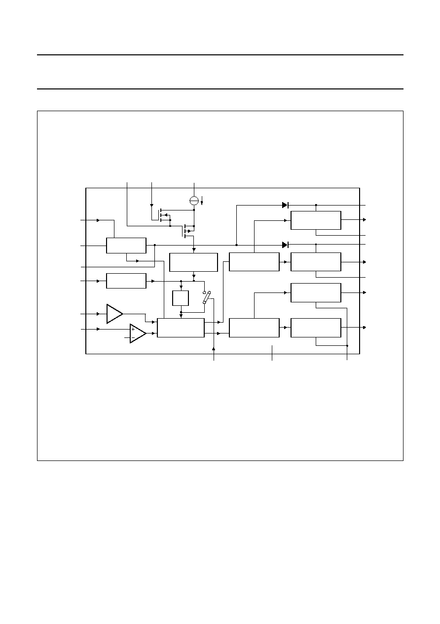
BLOCK DIAGRAM
handbook, full pagewidth
MBL457
LOW VOLTAGE
LEVEL SHIFTER
OSCILLATOR
STABILIZER
UVLO
HV
SGND
VDD
RC
SU
BD
HIGH VOLTAGE
LEVEL SHIFTER
HIGHER LEFT
DRIVER
LOWER RIGHT
DRIVER
LOWER LEFT
DRIVER
HIGHER RIGHT
DRIVER
LOGIC SIGNAL
GENERATOR
LOGIC
2
13
10
12
11
1.29 V
2
1
3
EXTDR
+
LVS
-
LVS
DD
4, 5, 7, 8, 18,
19, 22, 24, 25
n.c.
20
GLL
21
PGND
23
GLR
26
SHR
28
GHR
15
GHL
27
FSR
17
SHL
16
FSL
UBA2033TS
14
9
6
bridge disable
Fig.1 Block diagram.
2002 Oct 08
4
Philips Semiconductors
Product specification
HF full bridge driver IC
UBA2033
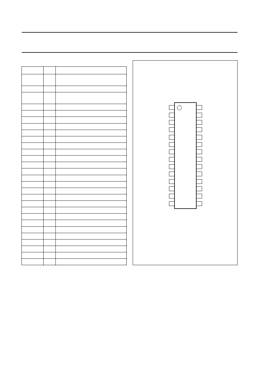
PINNING
SYMBOL
PIN
DESCRIPTION
-
LVS
1
negative supply voltage (for logic
input)
EXTDR
2
oscillator signal input
+
LVS
3
positive supply voltage (for logic
input)
n.c.
4
not connected
n.c.
5
not connected
HV
6
high voltage supply input
n.c.
7
not connected
n.c.
8
not connected
V
DD
9
internal low voltage supply
SU
10
input signal for start-up delay
DD
11
divider disable input
BD
12
bridge disable control input
RC
13
RC input for internal oscillator
SGND
14
signal ground
GHL
15
gate of higher left output MOSFET
FSL
16
floating supply voltage left
SHL
17
source of higher left MOSFET
n.c.
18
not connected
n.c.
19
not connected
GLL
20
gate of lower left output MOSFET
PGND
21
power ground
n.c.
22
not connected
GLR
23
gate of lower right output MOSFET
n.c.
24
not connected
n.c.
25
not connected
SHR
26
source of higher right MOSFET
FSR
27
floating supply voltage right
GHR
28
gate of higher right output MOSFET
handbook, halfpage
UBA2033TS
MBL458
1
2
3
4
5
6
7
8
9
10
11
12
13
14
28
27
26
25
24
23
22
21
20
19
18
17
16
15
EXTDR
n.c.
n.c.
HV
n.c.
n.c.
VDD
SU
DD
BD
RC
SGND
GHR
FSR
SHR
n.c.
n.c.
GLR
n.c.
PGND
GLL
n.c.
n.c.
SHL
FSL
GHL
+
LVS
-
LVS
Fig.2 Pin configuration.

2002 Oct 08
5
Philips Semiconductors
Product specification
HF full bridge driver IC
UBA2033
FUNCTIONAL DESCRIPTION
Supply voltage
The UBA2033 is powered by a supply voltage applied to
pin HV, for instance the supply voltage of the full bridge.
The IC generates its own low supply voltage for the
internal circuitry. Therefore an additional low voltage
supply is not required. A capacitor has to be connected to
pin V
DD
to obtain a ripple-free internal supply voltage.
The circuit can also be powered by a low voltage supply
directly applied to pin V
DD
. In this case pin HV should be
connected to pin V
DD
or SGND.
Start-up
With an increasing supply voltage the IC enters the
start-up state; the higher power transistors are kept off and
the lower power transistors are switched on. During the
start-up state the bootstrap capacitors are charged and the
bridge output current is zero. The start-up state is defined
until V
DD
= V
DD(UVLO)
, where UVLO stands for Under
Voltage Lock-out. The state of the outputs during the
start-up phase is overruled by the bridge disable function.
Release of the power drive
At the moment the supply voltage on pin V
DD
or HV
exceeds the level of release power drive, the output
voltage of the bridge depends on the control signal on
pin EXTDR (see Table 1). The bridge position after
start-up, disable, or delayed start-up (via pin SU) depends
on the status of the pins DD and EXTDR. If pin DD = LOW
(divider enabled) the bridge will start in the pre-defined
position: pin GLR and pin GHL = HIGH and pin GLL and
pin GHR = LOW. If pin DD = HIGH (divider disabled) the
bridge position will depend on the status of pin EXTDR.
If the supply voltage on pin V
DD
or HV decreases and
drops below the reset level of power drive the IC enters the
start-up state again.
Oscillation
At the point where the supply voltage on pin HV crosses
the level of release power drive, the bridge begins
commutating between the following two defined states:
∑
Higher left and lower right MOSFETs on,
higher right and lower left MOSFETs off
∑
Higher left and lower right MOSFETs off,
higher right and lower left MOSFETs on.
The oscillation can take place in three different modes:
∑
Internal oscillator mode.
In this mode the bridge commutating frequency is
determined by the values of an external resistor (R
osc
)
and capacitor (C
osc
). In this mode pin EXTDR must be
connected to pin
+
LVS. To realize an accurate 50% duty
factor, the internal divider should be used. The internal
divider is enabled by connecting pin DD to SGND. Due
to the presence of the divider the bridge frequency
is half the oscillator frequency. The commutation of the
bridge will take place at the falling edge of the signal on
pin RC. To minimize the current consumption
pins
+
LVS,
-
LVS and EXTDR can be connected
together to either pin SGND or V
DD
. In this way the
current source in the logic voltage supply circuit is shut
off.
∑
External oscillator mode without the internal divider.
In the external oscillator mode the external source is
connected to pin EXTDR and pin RC is short-circuited to
pin SGND to disable the internal oscillator. If the internal
divider is disabled (pin DD = V
DD
) the duty factor of the
bridge output signal is determined by the external
oscillator signal and the bridge frequency equals the
external oscillator frequency.
∑
External oscillator mode with the internal divider.
The external oscillator mode can also be used with the
internal divider function enabled (pin RC and
pin DD = SGND). Due to the presence of the divider the
bridge frequency is half the external oscillator
frequency. The commutation of the bridge is triggered
by the falling edge of the EXTDR signal with respect to
V
-
LVS
.
The design equation for the bridge oscillator frequency is:
Non-overlap time
The non-overlap time is the time between turning off the
conducting pair of MOSFETs and turning on the next pair.
The non-overlap time is internally fixed to a very small
value, which allows an HID system to operate with a very
small phase difference between load current and full
bridge voltage (pins SHL and SHR). Especially when
igniting an HID lamp via a LC resonance circuit, a small
`dead time' is essential. The high maximum operating
frequency, together with a small `dead time', also gives the
opportunity to ignite the HID lamp at the third harmonic of
the full bridge voltage, thereby reducing costs in the
magnetic power components.
f
bridge
1
k
osc
R
osc
◊
C
osc
◊
(
)
--------------------------------------------------
=

2002 Oct 08
6
Philips Semiconductors
Product specification
HF full bridge driver IC
UBA2033
'Dead time' can be increased by adding a resistor (for
slowly turning on the full bridge power FETs) and a diode
(for quickly turning off the full bridge power FETs) in
parallel, both in series with the gate drivers (see Fig.3).
Divider function
If pin DD = SGND, then the divider function is
enabled/present. If the divider function is present there is
no direct relation between the position of the bridge output
and the status of pin EXTDR.
Start-up delay
Normally, the circuit starts oscillating as soon as pin V
DD
or
HV reaches the level of release power drive. At this
moment the gate drive voltage is equal to the voltage on
pin V
DD
for the low side transistors and V
DD
-
0.6 V for the
high side transistors. If this voltage is too low for sufficient
drive of the MOSFETs the release of the power drive can
be delayed via pin SU.
A simple RC filter (R between pins V
DD
and SU;
C between pins SU and SGND) can be used to make a
delay, or a control signal from a processor can be used.
Bridge disable
The bridge disable function can be used to switch off all the
MOSFETs as soon as the voltage on pin BD exceeds the
bridge disable voltage (1.29 V). The bridge disable
function overrules all the other states.
Table 1
Logic table; note 1
Note
1. X = don't care
a) BD, SU and DD logic levels are with respect to SGND
b) EXTDR logic levels are with respect to V
-
LVS
c) GHL logic levels are with respect to SHL
d) GHR logic levels are with respect to SHR
e) GLL and GLR logic levels are with respect to PGND
f) If pin DD = LOW the bridge enters the state (oscillation state and pin BD = LOW and pin SU = HIGH) in the
pre-defined position pin GHL and pin GLR = HIGH and pin GLL and pin GHR = LOW.
DEVICE
STATUS
INPUTS
OUTPUTS
BD
SU
DD
EXTDR
GHL
GHR
GLL
GLR
Start-up state
HIGH
X
X
X
LOW
LOW
LOW
LOW
LOW
X
X
X
LOW
LOW
HIGH
HIGH
Oscillation state
HIGH
X
X
X
LOW
LOW
LOW
LOW
LOW
LOW
X
X
LOW
LOW
HIGH
HIGH
LOW
HIGH
HIGH
HIGH
LOW
HIGH
HIGH
LOW
LOW
HIGH
LOW
LOW
HIGH
LOW
HIGH
LOW
LOW
HIGH
LOW
LOW
HIGH
LOW-to-HIGH
HIGH
HIGH-to-LOW
LOW
HIGH
HIGH
LOW

2002 Oct 08
7
Philips Semiconductors
Product specification
HF full bridge driver IC
UBA2033
LIMITING VALUES
In accordance with the Absolute Maximum Rating System (IEC 60134); all voltages are measured with respect to
SGND; positive currents flow into the IC.
Note
1. In accordance with the Human Body Model (HBM): equivalent to discharging a 100 pF capacitor through a 1.5 k
series resistor.
SYMBOL
PARAMETER
CONDITIONS
MIN.
MAX.
UNIT
V
DD
supply voltage (low voltage)
DC value
0
14
V
transient at t < 0.1
µ
s
0
17
V
V
HV
supply voltage (high voltage)
0
550
V
V
FSL
floating supply voltage left
V
SHL
= V
SHR
= 550 V
0
564
V
V
SHL
= V
SHR
= 0 V
0
14
V
V
FSR
floating supply voltage right
V
SHL
= V
SHR
= 550 V
0
564
V
V
SHL
= V
SHR
= 0 V
0
14
V
V
SHL
source voltage for higher left
MOSFETs
with respect to PGND and SGND
-
3
+550
V
with respect to SGND; t < 1
µ
s
-
14
-
V
V
SHR
source voltage for higher right
MOSFETs
with respect to PGND and SGND
-
3
+550
V
with respect to SGND; t < 1
µ
s
-
14
-
V
V
PGND
power ground voltage
with respect to SGND
0
5
V
V
-
LVS
negative supply voltage for logic input
-
0.9
+17
V
I
-
LVS
negative supply current for logic input pin EXTDR = HIGH
-
1
-
mA
V
+
LVS
positive supply voltage for logic input
V
HV
= 0 V; DC value
0
14
V
transient at t < 0.1
µ
s
0
17
V
V
i(EXTDR)
input voltage from external oscillator
on pin EXTDR
with respect to V
-
LVS
0
V
+
LVS
V
V
i(RC)
input voltage on pin RC
DC value
0
V
DD
V
transient at t < 0.1
µ
s
0
17
V
V
i(SU)
input voltage on pin SU
DC value
0
V
DD
V
transient at t < 0.1
µ
s
0
17
V
V
i(BD)
input voltage on pin BD
DC value
0
V
DD
V
transient at t < 0.1
µ
s
0
17
V
V
i(DD)
input voltage on pin DD
DC value
0
V
DD
V
transient at t < 0.1
µ
s
0
17
V
SR
slew rate at output pins
repetitive
0
4
V/ns
T
j
junction temperature
-
40
+150
∞
C
T
amb
ambient temperature
-
40
+150
∞
C
T
stg
storage temperature
-
55
+150
∞
C
V
esd
electrostatic discharge voltage on
pins HV,
+
LVS,
-
LVS, EXTDR, FSL,
GHL, SHL, SHR, GHR and FSR
note 1
-
900
V

2002 Oct 08
8
Philips Semiconductors
Product specification
HF full bridge driver IC
UBA2033
THERMAL CHARACTERISTICS
QUALITY SPECIFICATION
In accordance with
"SNW-FQ-611D".
CHARACTERISTICS
T
j
= 25
∞
C; all voltages are measured with respect to SGND; positive currents flow into the IC; unless otherwise
specified.
SYMBOL
PARAMETER
CONDITIONS
VALUE
UNIT
R
th(j-a)
thermal resistance from junction to ambient
in free air
100
K/W
SYMBOL
PARAMETER
CONDITIONS
MIN.
TYP.
MAX.
UNIT
High voltage
I
HV
high voltage supply current
t < 0.5 s and V
HV
= 550 V
0
-
30
µ
A
I
FSL
, I
FSR
high voltage floating supply
current
t < 0.5 s and V
FSL
= V
FSR
= 564 V
0
-
30
µ
A
Start-up; powered via pin HV
I
i(HV)
HV input current
V
HV
= 11 V; note 1
-
0.5
1.0
mA
V
HV(rel)
level of release power drive
voltage
11
12.5
14
V
V
HV(UVLO)
reset level of power drive voltage
8.5
10
11.5
V
V
HV(hys)
HV hysteresis voltage
2.0
2.5
3.0
V
V
DD
internal supply voltage
V
HV
= 20 V
10.5
11.5
13.5
V
Start-up; powered via pin V
DD
I
i(DD)
V
DD
input current
V
DD
= 8.25 V; note 2
-
0.5
1.0
mA
V
DD(rel)
level of release power drive
voltage
8.25
9.0
9.75
V
V
DD(UVLO)
reset level of power drive voltage
5.75
6.5
7.25
V
V
DD(hys)
hysteresis voltage
2.0
2.5
3.0
V
Output stage
R
on(H)
higher MOSFETs on resistance
V
FSR
= V
FSL
= 12 V (with respect
to SHR and SHL); I
source
= 50 mA
15
21
26
R
off(H)
higher MOSFETs off resistance
V
FSR
= V
FSL
= 12 V (with respect
to SHR and SHL); I
sink
= 50 mA
9
14
18
R
on(L)
lower MOSFETs on resistance
V
DD
= 12 V; I
source
= 50 mA
15
21
26
R
off(L)
lower MOSFETs off resistance
V
DD
= 12 V; I
sink
= 50 mA
9
14
18
I
o(source)
output source current
V
DD
= V
FSL
= V
FSR
= 12 V;
V
GHR
= V
GHL
= V
GLR
= V
GLL
= 0 V
130
180
-
mA
I
o(sink)
output sink current
V
DD
= V
FSL
= V
FSR
= 12 V;
V
GHR
= V
GHL
= V
GLR
= V
GLL
= 12 V
150
200
-
mA
V
diode
bootstrap diode voltage drop
I
diode
= 20 mA
1.7
2.1
2.5
V
t
no
non-overlap time
-
-
250
ns
V
FSL
HS lockout voltage left
3.0
4.0
5.0
V

2002 Oct 08
9
Philips Semiconductors
Product specification
HF full bridge driver IC
UBA2033
Notes
1. The current is specified without commutation of the bridge. The current into pin HV is limited by a thermal protection
circuit. The current is limited to 11 mA at T
j
= 150
∞
C.
2. The current is specified without commutation of the bridge and pin HV is connected to V
DD
.
3. The minimum frequency is mainly determined by the value of the bootstrap capacitors.
V
FSR
HS lockout voltage right
3.0
4.0
5.0
V
I
FSL
FS supply current left
V
FSL
= 12 V
2
4
6
µ
A
I
FSR
FS supply current right
V
FSR
= 12 V
2
4
6
µ
A
DD input
V
IH
HIGH-level input voltage
V
DD
= 12 V
6
-
-
V
V
IL
LOW-level input voltage
-
-
3
V
I
i(DD)
input current into pin DD
-
-
1
µ
A
SU input
V
IH
HIGH-level input voltage
V
DD
= 12 V
4
-
-
V
V
IL
LOW-level input voltage
-
-
2
V
I
i(SU)
input current into pin SU
-
-
1
µ
A
External drive input
V
IH
HIGH-level input voltage
with respect to V
-
LVS
4.0
-
-
V
V
IL
LOW-level input voltage
with respect to V
-
LVS
-
-
1.0
V
I
i(EXTDR)
input current into pin EXTDR
-
-
1
µ
A
f
bridge
bridge frequency
note 3
-
-
250
kHz
Low voltage logic supply
I
+
LVS
low voltage supply current
V
+
LVS
= V
EXTDR
= 5.75 to 14 V with
respect to V
-
LVS
-
250
500
µ
A
V
+
LVS
low voltage supply voltage
with respect to V
-
LVS
5.75
-
14
V
Bridge disable input
V
ref(dis)
disable reference voltage
1.23
1.29
1.35
V
I
i(BD)
disable input current
-
-
1
µ
A
Internal oscillator
f
bridge
bridge oscillating frequency
note 3
-
-
100
kHz
f
osc(T)
oscillator frequency variation
with temperature
f
bridge
= 250 Hz and
T
amb
=
-
40 to +150
∞
C
-
10
0
+10
%
f
osc(VDD)
oscillator frequency variation
with V
DD
f
bridge
= 250 Hz and
V
DD
= 7.25 to 14 V
-
10
0
+10
%
k
H
high level trip point
V
RC(high)
= k
H
◊
V
DD
0.38
0.4
0.42
k
L
low level trip point
V
RC(low)
= k
L
◊
V
DD
-
0.01
-
k
osc
oscillator constant
f
bridge
= 250 Hz
0.94
1.02
1.10
R
ext
external resistor to V
DD
100
-
-
k
SYMBOL
PARAMETER
CONDITIONS
MIN.
TYP.
MAX.
UNIT

2002 Oct 08
10
Philips Semiconductors
Product specification
HF full bridge driver IC
UBA2033
APPLICATION INFORMATION
Basic application
A basic full bridge configuration with an HID lamp is shown
in Fig.3. The bridge disable, the start-up delay and the
external drive functions are not used in this application.
The pins
-
LVS,
+
LVS, EXTDR and BD are short-circuited
to SGND. The internal oscillator is used and to realize a
50% duty cycle the internal divider function has to be used
by connecting pin DD to SGND. The IC is powered by the
high voltage supply. Because the internal oscillator is
used, the bridge commutating frequency is determined by
the values of R
osc
and C
osc
. The bridge starts oscillating
when the HV supply voltage exceeds the level of release
power drive (typically 12.5 V on pin HV). If the supply
voltage on pin HV drops below the reset level of power
drive (typically 10 V on pin HV), the UBA2033 enters the
start-up state.
handbook, full pagewidth
UBA2033TS
VDD
EXTDR
SGND
HV
SU
DD
BD
RC
GHR
FSR
SHR
GLR
R>100
R>100
R>100
R>100
GLL
SHL
FSL
GHL
PGND
1
2
3
6
9
10
11
12
13
14
28
27
26
23
21
20
17
16
15
IGNITOR
Ci
C3
C1
C2
Rosc
Cosc
LR
HR
LL
HL
high voltage
550 V (max)
GND
MBL459
+
LVS
-
LVS
Fig.3 Basic configuration.

2002 Oct 08
11
Philips Semiconductors
Product specification
HF full bridge driver IC
UBA2033
Application with external control
Figure 4 shows an application containing a system
ground-referenced control circuit. Pin
+
LVS can be
connected to the same supply as the external oscillator
control unit and pin
-
LVS is connected to SGND. Pin RC is
short-circuited to SGND. The bridge commutation
frequency is determined by the external oscillator. The
bridge disable input (pin BD) can be used to immediately
turn off all four MOSFETs in the full bridge.
handbook, full pagewidth
UBA2033TS
VDD
EXTDR
SGND
HV
SU
DD
BD
RC
GHR
FSR
SHR
GLR
R>100
R>100
R>100
R>100
GLL
SHL
FSL
GHL
PGND
1
2
3
6
9
10
11
12
13
14
28
27
26
23
21
20
17
16
15
IGNITOR
Ci
C1
C2
C3
LR
HR
LL
HL
high voltage
550 V (max)
GND
MBL460
EXTERNAL
OSCILLATOR
CONTROL
CIRCUIT
low voltage
+
LVS
-
LVS
Fig.4 External control configuration.

2002 Oct 08
12
Philips Semiconductors
Product specification
HF full bridge driver IC
UBA2033
Additional application information
G
ATE RESISTORS
At ignition of an HID lamp, a large EMC spark occurs. This
can result in a large voltage transient or oscillation at the
gates of the full bridge MOSFETs (LL, LR, HR and HL).
When these gates are directly coupled to the gate drivers
(pins GHR, GLR, GHL and GLL), voltage overstress of the
driver outputs may occur. Therefore it is advised to add a
resistor with a minimum value of 100
in series with each
gate driver to isolate the gate driver outputs from the actual
power MOSFETs gate.
'Dead time' can also be adjusted via the combination gate
resistor and gate-source capacitance.
G
ATE CHARGE AND SUPPLY CURRENT AT HIGH FREQUENCY
USE
The total gate current needed to charge the gates of the
power MOSFETs equals:
Where:
I
gate
= gate current
f
bridge
= bridge frequency
Q
gate
= gate charge.
This current is supplied via the internal low voltage supply
(V
DD
). Since this current is limited to 11 mA (see
"Characteristics" table note 1), at higher frequencies and
with MOSFETs having a relative high gate charge, this
maximum V
DD
supply current may not be sufficient
anymore. As a result the internal low voltage supply (V
DD
)
and the gate drive voltage will drop resulting in an increase
of the higher resistance (R
on
) of the full bridge MOSFETs.
In this case an auxiliary low voltage supply is necessary.
I
gate
4
f
bridge
Q
gate
◊
◊
=
2002 Oct 08
13
Philips Semiconductors
Product specification
HF full bridge driver IC
UBA2033
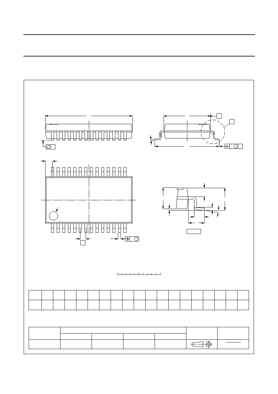
PACKAGE OUTLINE
UNIT
A
1
A
2
A
3
b
p
c
D
(1)
E
(1)
(1)
e
H
E
L
L
p
Q
Z
y
w
v
REFERENCES
OUTLINE
VERSION
EUROPEAN
PROJECTION
ISSUE DATE
IEC
JEDEC
EIAJ
mm
0.21
0.05
1.80
1.65
0.38
0.25
0.20
0.09
10.4
10.0
5.4
5.2
0.65
1.25
7.9
7.6
0.9
0.7
1.1
0.7
8
0
o
o
0.13
0.1
0.2
DIMENSIONS (mm are the original dimensions)
Note
1. Plastic or metal protrusions of 0.20 mm maximum per side are not included.
1.03
0.63
SOT341-1
MO-150
95-02-04
99-12-27
X
w
M
A
A
1
A
2
b
p
D
H
E
L
p
Q
detail X
E
Z
e
c
L
v
M
A
(A )
3
A
1
14
28
15
0.25
y
pin 1 index
0
2.5
5 mm
scale
SSOP28: plastic shrink small outline package; 28 leads; body width 5.3 mm
SOT341-1
A
max.
2.0

2002 Oct 08
14
Philips Semiconductors
Product specification
HF full bridge driver IC
UBA2033
SOLDERING
Introduction to soldering surface mount packages
This text gives a very brief insight to a complex technology.
A more in-depth account of soldering ICs can be found in
our
"Data Handbook IC26; Integrated Circuit Packages"
(document order number 9398 652 90011).
There is no soldering method that is ideal for all surface
mount IC packages. Wave soldering can still be used for
certain surface mount ICs, but it is not suitable for fine pitch
SMDs. In these situations reflow soldering is
recommended.
Reflow soldering
Reflow soldering requires solder paste (a suspension of
fine solder particles, flux and binding agent) to be applied
to the printed-circuit board by screen printing, stencilling or
pressure-syringe dispensing before package placement.
Several methods exist for reflowing; for example,
convection or convection/infrared heating in a conveyor
type oven. Throughput times (preheating, soldering and
cooling) vary between 100 and 200 seconds depending
on heating method.
Typical reflow peak temperatures range from
215 to 250
∞
C. The top-surface temperature of the
packages should preferable be kept below 220
∞
C for
thick/large packages, and below 235
∞
C for small/thin
packages.
Wave soldering
Conventional single wave soldering is not recommended
for surface mount devices (SMDs) or printed-circuit boards
with a high component density, as solder bridging and
non-wetting can present major problems.
To overcome these problems the double-wave soldering
method was specifically developed.
If wave soldering is used the following conditions must be
observed for optimal results:
∑
Use a double-wave soldering method comprising a
turbulent wave with high upward pressure followed by a
smooth laminar wave.
∑
For packages with leads on two sides and a pitch (e):
≠ larger than or equal to 1.27 mm, the footprint
longitudinal axis is preferred to be parallel to the
transport direction of the printed-circuit board;
≠ smaller than 1.27 mm, the footprint longitudinal axis
must be parallel to the transport direction of the
printed-circuit board.
The footprint must incorporate solder thieves at the
downstream end.
∑
For packages with leads on four sides, the footprint must
be placed at a 45
∞
angle to the transport direction of the
printed-circuit board. The footprint must incorporate
solder thieves downstream and at the side corners.
During placement and before soldering, the package must
be fixed with a droplet of adhesive. The adhesive can be
applied by screen printing, pin transfer or syringe
dispensing. The package can be soldered after the
adhesive is cured.
Typical dwell time is 4 seconds at 250
∞
C.
A mildly-activated flux will eliminate the need for removal
of corrosive residues in most applications.
Manual soldering
Fix the component by first soldering two
diagonally-opposite end leads. Use a low voltage (24 V or
less) soldering iron applied to the flat part of the lead.
Contact time must be limited to 10 seconds at up to
300
∞
C.
When using a dedicated tool, all other leads can be
soldered in one operation within 2 to 5 seconds between
270 and 320
∞
C.

2002 Oct 08
15
Philips Semiconductors
Product specification
HF full bridge driver IC
UBA2033
Suitability of surface mount IC packages for wave and reflow soldering methods
Notes
1. All surface mount (SMD) packages are moisture sensitive. Depending upon the moisture content, the maximum
temperature (with respect to time) and body size of the package, there is a risk that internal or external package
cracks may occur due to vaporization of the moisture in them (the so called popcorn effect). For details, refer to the
Drypack information in the
"Data Handbook IC26; Integrated Circuit Packages; Section: Packing Methods".
2. These packages are not suitable for wave soldering. On versions with the heatsink on the bottom side, the solder
cannot penetrate between the printed-circuit board and the heatsink. On versions with the heatsink on the top side,
the solder might be deposited on the heatsink surface.
3. If wave soldering is considered, then the package must be placed at a 45
∞
angle to the solder wave direction.
The package footprint must incorporate solder thieves downstream and at the side corners.
4. Wave soldering is only suitable for LQFP, TQFP and QFP packages with a pitch (e) equal to or larger than 0.8 mm;
it is definitely not suitable for packages with a pitch (e) equal to or smaller than 0.65 mm.
5. Wave soldering is only suitable for SSOP and TSSOP packages with a pitch (e) equal to or larger than 0.65 mm; it is
definitely not suitable for packages with a pitch (e) equal to or smaller than 0.5 mm.
PACKAGE
SOLDERING METHOD
WAVE
REFLOW
(1)
BGA, HBGA, LFBGA, SQFP, TFBGA
not suitable
suitable
HBCC, HLQFP, HSQFP, HSOP, HTQFP, HTSSOP, HVQFN, SMS
not suitable
(2)
suitable
PLCC
(3)
, SO, SOJ
suitable
suitable
LQFP, QFP, TQFP
not recommended
(3)(4)
suitable
SSOP, TSSOP, VSO
not recommended
(5)
suitable

2002 Oct 08
16
Philips Semiconductors
Product specification
HF full bridge driver IC
UBA2033
DATA SHEET STATUS
Notes
1. Please consult the most recently issued data sheet before initiating or completing a design.
2. The product status of the device(s) described in this data sheet may have changed since this data sheet was
published. The latest information is available on the Internet at URL http://www.semiconductors.philips.com.
3. For data sheets describing multiple type numbers, the highest-level product status determines the data sheet status.
LEVEL
DATA SHEET
STATUS
(1)
PRODUCT
STATUS
(2)(3)
DEFINITION
I
Objective data
Development
This data sheet contains data from the objective specification for product
development. Philips Semiconductors reserves the right to change the
specification in any manner without notice.
II
Preliminary data Qualification
This data sheet contains data from the preliminary specification.
Supplementary data will be published at a later date. Philips
Semiconductors reserves the right to change the specification without
notice, in order to improve the design and supply the best possible product.
III
Product data
Production
This data sheet contains data from the product specification. Philips
Semiconductors reserves the right to make changes at any time in order to
improve the design, manufacturing and supply. Relevant changes will be
communicated via a Customer Product/Process Change Notification
(CPCN).
DEFINITIONS
Short-form specification
The data in a short-form
specification is extracted from a full data sheet with the
same type number and title. For detailed information see
the relevant data sheet or data handbook.
Limiting values definition
Limiting values given are in
accordance with the Absolute Maximum Rating System
(IEC 60134). Stress above one or more of the limiting
values may cause permanent damage to the device.
These are stress ratings only and operation of the device
at these or at any other conditions above those given in the
Characteristics sections of the specification is not implied.
Exposure to limiting values for extended periods may
affect device reliability.
Application information
Applications that are
described herein for any of these products are for
illustrative purposes only. Philips Semiconductors make
no representation or warranty that such applications will be
suitable for the specified use without further testing or
modification.
DISCLAIMERS
Life support applications
These products are not
designed for use in life support appliances, devices, or
systems where malfunction of these products can
reasonably be expected to result in personal injury. Philips
Semiconductors customers using or selling these products
for use in such applications do so at their own risk and
agree to fully indemnify Philips Semiconductors for any
damages resulting from such application.
Right to make changes
Philips Semiconductors
reserves the right to make changes in the products -
including circuits, standard cells, and/or software -
described or contained herein in order to improve design
and/or performance. When the product is in full production
(status `Production'), relevant changes will be
communicated via a Customer Product/Process Change
Notification (CPCN). Philips Semiconductors assumes no
responsibility or liability for the use of any of these
products, conveys no licence or title under any patent,
copyright, or mask work right to these products, and
makes no representations or warranties that these
products are free from patent, copyright, or mask work
right infringement, unless otherwise specified.

2002 Oct 08
17
Philips Semiconductors
Product specification
HF full bridge driver IC
UBA2033
NOTES

2002 Oct 08
18
Philips Semiconductors
Product specification
HF full bridge driver IC
UBA2033
NOTES

2002 Oct 08
19
Philips Semiconductors
Product specification
HF full bridge driver IC
UBA2033
NOTES

© Koninklijke Philips Electronics N.V. 2002
SCA74
All rights are reserved. Reproduction in whole or in part is prohibited without the prior written consent of the copyright owner.
The information presented in this document does not form part of any quotation or contract, is believed to be accurate and reliable and may be changed
without notice. No liability will be accepted by the publisher for any consequence of its use. Publication thereof does not convey nor imply any license
under patent- or other industrial or intellectual property rights.
Philips Semiconductors ≠ a worldwide company
Contact information
For additional information please visit http://www.semiconductors.philips.com.
Fax: +31 40 27 24825
For sales offices addresses send e-mail to: sales.addresses@www.semiconductors.philips.com.
Printed in The Netherlands
613502/01/pp
20
Date of release:
2002 Oct 08
Document order number:
9397 750 09574