Document Outline
- FEATURES
- APPLICATION
- GENERAL DESCRIPTION
- ORDERING INFORMATION
- QUICK REFERENCE DATA
- BLOCK DIAGRAM
- PINNING
- FUNCTIONAL DESCRIPTION
- LIMITING VALUES
- THERMAL CHARACTERISTICS
- QUALITY SPECIFICATION
- CHARACTERISTICS
- PACKAGE OUTLINE
- SOLDERING
- DEFINITIONS
- LIFE SUPPORT APPLICATIONS

DATA SHEET
Product specification
Supersedes data of 1996 Jul 18
File under Integrated Circuits, IC01
1998 Jan 06
INTEGRATED CIRCUITS
UDA1309H
Low-power stereo bitstream
ADC/DAC

1998 Jan 06
2
Philips Semiconductors
Product specification
Low-power stereo bitstream ADC/DAC
UDA1309H
FEATURES
∑
Low power
∑
Integrated high-pass filter to cancel DC offset (ADC)
∑
Analog loop-through function
∑
Multiple digital input/output formats possible
∑
256f
s
system clock frequency
∑
Several power-down modes
∑
Digital de-emphasis (DAC)
∑
Overload detector to enable automatic recording level
adjustment (ADC)
∑
High dynamic range
∑
DAC requires only one capacitor for post-filtering
∑
Small 44-pin quad flat pack with 0.8 mm pitch
∑
256f
s
system clock frequency in Analog-to-Digital (AD)
and Digital-to-Analog (DA) mode
∑
Choice of three system clock frequencies
(192f
s
, 256f
s
or 384f
s
) in DA mode.
APPLICATION
∑
Portable digital audio equipment.
GENERAL DESCRIPTION
The UDA1309H is a single chip stereo analog-to-digital
and digital-to-analog converter employing bitstream
conversion techniques. The device is eminently suitable
for use in low-power portable digital audio equipment
which incorporates recording and playback functions.
ORDERING INFORMATION
TYPE
NUMBER
PACKAGE
NAME
DESCRIPTION
VERSION
UDA1309H
QFP44 plastic quad flat package; 44 leads (lead length 1.3 mm); body 10
◊
10
◊
1.75 mm SOT307-2

1998 Jan 06
3
Philips Semiconductors
Product specification
Low-power stereo bitstream ADC/DAC
UDA1309H
QUICK REFERENCE DATA
V
DDD
= V
DDA
= V
DDO
= V
DDD(F)
= 5 V; V
SSD
= V
SSA
= V
SSO
= V
SSD(F)
= 0 V; T
amb
= 25
∞
C; full scale sine wave input;
mode 1; f
i
= 1 kHz; 16-bit input data; conversion rate = 44.1 kHz; measurement bandwidth = 10 Hz to 20 kHz; unless
otherwise specified.
Notes
1. V
I
for full scale digital output is a function of V
DDA(AD)
[1.0 V (RMS) at V
DDA(AD)
= 5.0 V is equivalent to
-
1.0 dB in the
digital domain].
2. At full scale digital input; no de-emphasis; V
O(rms)
is a function of V
DDA(DA)
.
3. 18-bit input data.
SYMBOL
PARAMETER
CONDITIONS
MIN.
TYP.
MAX. UNIT
Supply
V
DDA(AD)
ADC analog supply voltage (pin 8)
4.5
5.0
5.5
V
V
DDA(DA)
DAC analog supply voltage (pin 25)
4.5
5.0
5.5
V
V
DDO
operational amplifiers supply voltage
(pin 19)
4.5
5.0
5.5
V
V
DDD
ADC and DAC digital supply voltage
(pin 28)
4.5
5.0
5.5
V
V
DDD(F)
digital filters supply voltage (pin 34)
4.5
5.0
5.5
V
I
DDA(AD)
ADC analog supply current (pin 8)
-
9
13.5
mA
I
DDA(DA)
DAC analog supply current (pin 25)
-
4.5
6.8
mA
I
DDO
operational amplifiers supply current
(pin 19)
-
14
21
mA
I
DDD
ADC and DAC digital supply current
(pin 28)
-
0.2
0.5
mA
I
DDD(F)
digital filters supply current (pin 34)
-
24
36
mA
T
amb
operating ambient temperature
-
20
-
+75
∞
C
Analog-to-digital converter
V
I(rms)
input voltage (RMS value)
note 1
0.9
1.0
1.1
V
(THD + N)/S total harmonic distortion plus
noise-to-signal ratio
at 0 dB
-
-
85
tbf
dB
at
-
60 dB; A-weighted
-
-
35
-
30
dB
S/N
idle channel signal-to-noise ratio
V
I
= 0 V; A-weighted
tbf
95
-
dB
cs
channel separation
-
90
-
dB
Digital-to-analog converter
V
O(rms)
output voltage (RMS value)
note 2
0.9
1.0
1.1
V
(THD + N)/S total harmonic distortion plus
noise-to-signal ratio
at 0 dB
-
-
90
-
82
dB
at
-
60 dB; A-weighted
-
-
38
-
34
dB
at
-
60 dB; A-weighted; note 3
-
-
44
-
dB
S/N
idle channel signal-to-noise ratio
code 0000H; A-weighted
-
104
-
dB
cs
channel separation
90
100
-
dB
1998 Jan 06
4
Philips Semiconductors
Product specification
Low-power stereo bitstream ADC/DAC
UDA1309H
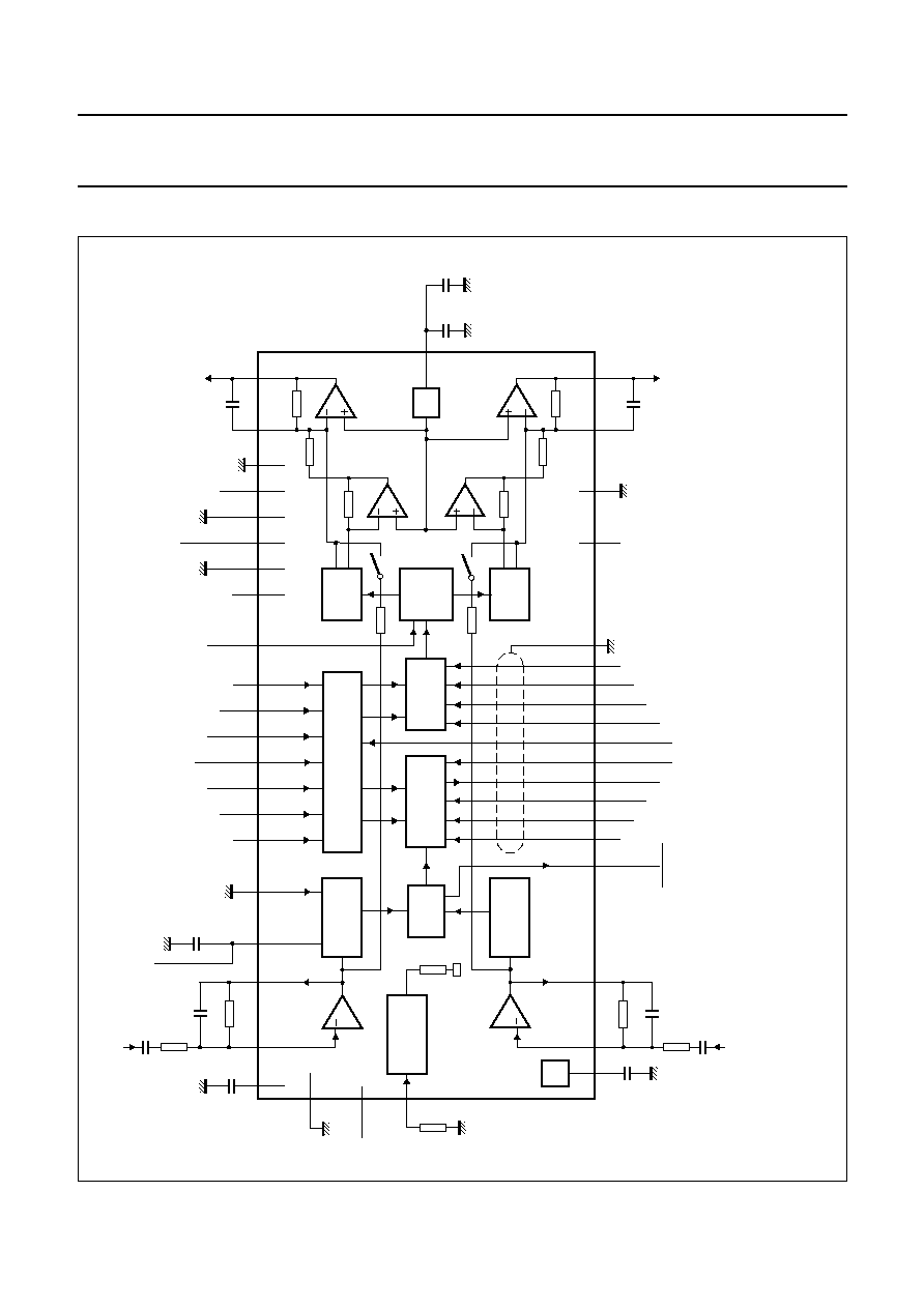
BLOCK DIAGRAM
ook, full pagewidth
MBH527
4.7 k
4.7 k
4.7 k
4.7 k
1.6 k
1.6 k
47
µ
F
0.22
µ
F
0.22
µ
F
47
µ
F
0.22
µ
F
1 nF
1 nF
330 pF
330 pF
47
k
10
µ
F
0.22
µ
F
Vm
Vm
DAC
DIGITAL
FILTER
DIGITAL
FILTER
DAC
DIGITAL
INTERFACE
DIGITAL
INTERFACE
MODE SELECT
ADC
ADC
CURRENT
REFERENCE
14
15
42
1
41
6
36
32
31
35
29
5
39
28
27
23
24
18
22
21
19
20
26
25
33
34
30
3
42
43
44
37
38
40
9
11
12
13
10
16
7
8
17
AD
ref
BAIR
BA
OR
O
VLO
AD
ADENB
AD
WS
ADBCK
ADSD
A
ADPON
ANLPTR
DA
W
S
D
ABCK
D
ASD
A
D
APON
V
SS(I/O)
V
DDD
V
SSD
DA
C
R
V
OR
analog output
V
OR
DA
ref
analog input
V
IR
V
OL
DACL
analog output
V
OL
V
SSO
V
DDO
V
SSA(DA)
V
DDA(DA)
V
SSD(F)
V
DDD(F)
DADEM
MODE0
MODE1
MODE2
CLKEDGE
TEST0
TEST1
SYSCLK
V
ref(neg)
V
ref(pos)
BAOL
BAIL
V
ref
V
DDA(AD)
analog input
V
IL
V
SSA(AD)
V
DDA(AD)
I ref
I DAC
UDA1309H
Supply decoupling on pins 19, 25, 28 and 34; 0.22
µ
F (ceramic), 47
µ
F (electrolytic).
Capacitance at pin 11 should be close to pins 11 and 9.
Fig.1 Block diagram.

1998 Jan 06
5
Philips Semiconductors
Product specification
Low-power stereo bitstream ADC/DAC
UDA1309H
PINNING
SYMBOL
PIN
DESCRIPTION
ADBCK
1
ADC input bit clock; 32f
s
or 64f
s
ADWS
2
ADC word select input at f
s
MODE0
3
ADC/DAC mode select input
ADENB
4
ADC serial data enable input (active HIGH)
OVLOAD
5
ADC output overload flag (active LOW)
ADPON
6
ADC power-on-mode input (active HIGH)
V
SSA(AD)
7
ADC analog ground supply voltage
V
DDA(AD)
8
ADC analog supply voltage
V
ref(neg)
9
ADC negative reference voltage input (ground)
V
ref
10
ADC decoupling capacitor
V
ref(pos)
11
ADC positive reference voltage decoupling capacitor
BAOL
12
ADC input amplifier output left
BAIL
13
ADC input amplifier virtual ground left
BAIR
14
ADC input amplifier virtual ground right
BAOR
15
ADC input amplifier output right
AD
ref
16
ADC decoupling capacitor
I
ref
17
ADC/DAC reference current resistor input
DA
ref
18
DAC decoupling capacitor
V
DDO
19
ADC/DAC operational amplifier supply voltage
V
SSO
20
ADC/DAC operational amplifier ground supply voltage
V
OL
21
DAC output voltage left
DACL
22
DAC output current left
DACR
23
DAC output current right
V
OR
24
DAC output voltage right
V
DDA(DA)
25
DAC analog supply voltage
V
SSA(DA)
26
DAC analog ground supply voltage
V
SSD
27
ADC/DAC digital ground supply voltage
V
DDD
28
ADC/DAC digital supply voltage
DAPON
29
DAC power-on-mode input (active HIGH)
DADEM
30
DAC digital de-emphasis input (active HIGH)
DABCK
31
DAC input bit clock; 32f
s
, 48f
s
or 64f
s
DAWS
32
DAC word select input at f
s
V
SSD(F)
33
ADC/DAC digital filters ground supply voltage
V
DDD(F)
34
ADC/DAC digital filters supply voltage
DASDA
35
DAC serial data input
ANLPTR
36
ADC/DAC analog loop-through input (active HIGH)
TEST0
37
ADC/DAC enable test mode 0 input (LOW is normal mode)
TEST1
38
ADC/DAC enable test mode 1 input (LOW is normal mode)
V
SS(I/O)
39
ADC/DAC digital input/output ground supply voltage
SYSCLK
40
ADC/DAC system clock input (f
sys
= 256f
s
; DAC also 192f
s
and 384f
s
)