
1.
General description
The UJA1023 is a stand-alone Local Interconnect Network (LIN) I/O slave that replaces
basic components commonly used in electronic control units for input and output handling.
The UJA1023 contains a LIN 2.0 controller, an integrated LIN transceiver which is
LIN 2.0 / SAE J2602 compliant and LIN 1.3 compatible, a 30 k
termination resistor
necessary for LIN-slaves, and eight I/O ports which are configurable via the LIN bus.
An automatic bit rate synchronization circuit adapts to any (master) bit rate between
1 kbit/s and 20 kbit/s. For this, an oscillator is integrated.
The LIN protocol will be handled autonomously and both Node Address (NAD) and LIN
frame Identifier (ID) programming will be done by a master request and an optional slave
response message in combination with a daisy chain or plug coding function.
The eight bidirectional I/O pins are configurable via LIN bus messages and can have the
following functions:
�
Input:
� Standard input pin
� Local wake-up
� Edge capturing on falling, rising or both edges
� Analog input pin
� Switch matrix (in combination with output pins)
�
Output:
� Standard output pin as high-side driver, low-side driver or push-pull driver
� Cyclic sense mode for local wake-up
� PWM mode, for example, for back light illumination
� Switch matrix (in combination with input pins)
On entering a low-power mode it is possible to hold the last output state or to change over
to a user programmable output state. In case of a failure (e.g. LIN bus short to ground) the
output changes over to a user programmable limp home output state and the low-power
Limp home mode will be entered.
Due to the advanced low-power behavior the power consumption of the UJA1023 in
low-power mode is minimal.
UJA1023
LIN-I/O slave
Rev. 03 -- 9 February 2006
Preliminary data sheet

UJA1023_3
� Koninklijke Philips Electronics N.V. 2006. All rights reserved.
Preliminary data sheet
Rev. 03 -- 9 February 2006
2 of 50
Philips Semiconductors
UJA1023
LIN-I/O slave
2.
Features
s
Automatic bit rate synchronization to any (master) bit rate between 1 kbit/s
and 20 kbit/s
s
Integrated LIN 2.0 / SAE J2602 transceiver (including 30 k
termination resistor)
s
Eight bidirectional I/O pins
s
4
�
2, 4
�
3, or 4
�
4 switch matrix to support reading and supplying a maximum
number of 16 switches
s
Outputs configurable as high-side and/or low-side driver and as cyclic or PWM driver
s
8-bit ADC
s
Advanced low-power behavior
s
On-chip oscillator
s
Node Address (NAD) configuration via daisy chain or plug coding
s
Inputs supporting local wake-up and edge capturing
s
Configurable Sleep mode
s
Limp home configuration in case of error conditions
s
Extremely low electromagnetic emission
s
High immunity against electromagnetic interference
s
Bus line protected in accordance with ISO 7637
s
Extended ambient temperature range (
-
40
�
C to +125
�
C)
3.
Quick reference data
[1]
All outputs turned off, LIN recessive, V
th1
selected.
[2]
Junction temperature in accordance with IEC60747-1. An alternative definition of T
vj
= T
amb
+ P
�
R
th(j-a)
,
where R
th(j-a)
is a fixed value to be used for calculating T
vj
. The rating for T
vj
limits the allowable
combinations of power dissipation (P) and ambient temperature (T
amb
).
4.
Ordering information
Table 1:
Quick reference data
Symbol Parameter
Conditions
Min
Typ
Max
Unit
V
BAT
supply voltage on pin BAT
all operating modes
6.5
-
27
V
I
BAT
supply current on pin BAT
LH sleep, Sleep and
Limp home mode
[1]
-
45
65
�
A
V
LIN
voltage on pin LIN
DC value
-
27
-
+40
V
T
vj
virtual junction temperature
[2]
-
40
-
+150
�
C
V
esd
electrostatic discharge voltage
on pins LIN, BAT, C1, C2 and C3
human body model;
C = 100 pF; R = 1.5 k
-
8
-
+8
kV
Table 2:
Ordering information
Type number
Package
Name
Description
Version
UJA1023T
SO16
plastic small outline package; 16 leads;
body width 3.9 mm
SOT109-1
UJA1023_3
� Koninklijke Philips Electronics N.V. 2006. All rights reserved.
Preliminary data sheet
Rev. 03 -- 9 February 2006
3 of 50
Philips Semiconductors
UJA1023
LIN-I/O slave
5.
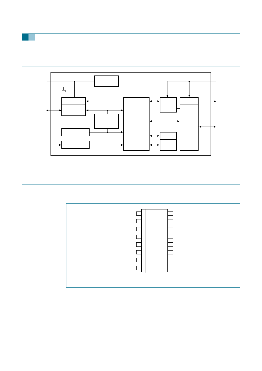
Block diagram
6.
Pinning information
6.1 Pinning
Fig 1.
Block diagram
mdb488
TERMINATION
OSCILLATOR
CYCLIC
SENSE
PWM
ADC
INH
I/O BLOCK
LIN
TRANSCEIVER
CONFIGURATION
AUTO
BIT RATE
DETECTION
VOLTAGE
REGULATOR
LIN
CONTROLLER
VIO
INH
P0 to P7
C1 to C3
LIN
BAT
GND
3
1
2
9 to 16
4
6 to 8
5
UJA1023
Fig 2.
Pin configuration
UJA1023T
VIO
P7
INH
P6
BAT
P5
LIN
P4
GND
P3
C1
P2
C2
P1
C3
P0
001aab877
1
2
3
4
5
6
7
8
10
9
12
11
14
13
16
15

UJA1023_3
� Koninklijke Philips Electronics N.V. 2006. All rights reserved.
Preliminary data sheet
Rev. 03 -- 9 February 2006
4 of 50
Philips Semiconductors
UJA1023
LIN-I/O slave
6.2 Pin description
[1]
I = input;
O = output;
I/O = input or output.
7.
Functional description
The UJA1023 combines all blocks necessary to work as a stand-alone LIN slave. Various
I/O functions typically used in a car are supported. For a more detailed description refer to
Section 7.2
to
Section 7.6
. The block diagram is shown in
Figure 1
.
7.1 Short description of the UJA1023
7.1.1 LIN controller
The LIN 2.0 controller monitors and evaluates the LIN messages in order to process the
LIN commands. It supervises and executes the NAD assignment, ID assignment and
I/O-configuration and controls the operating modes of the UJA1023.
The NAD configuration is done by a combination of a LIN master request frame and a
setting done by either a daisy chain or plug ID code.
7.1.2 LIN transceiver (including termination)
The LIN transceiver, which is LIN 2.0 / SAE J2602 compliant, is the interface between the
internal LIN controller and the physical LIN bus. The transmit data stream of the LIN
controller is converted into a bus signal with an optimized wave shape to minimize
Table 3:
Pin description
Symbol
Pin
Type
[1]
Description
VIO
1
I
reference input for level adaptation of the I/O pins P0 to P7
INH
2
O
inhibit output for controlling an external voltage regulator or
internal ADC
BAT
3
I
battery supply
LIN
4
I/O
LIN bus line
GND
5
I
ground
C1
6
I
configuration input 1 for LIN slave NAD assignment
C2
7
I
configuration input 2 for LIN slave NAD assignment
C3
8
I/O
configuration input / output 3 for LIN slave NAD assignment
P0
9
I/O
bidirectional I/O pin 0
P1
10
I/O
bidirectional I/O pin 1
P2
11
I/O
bidirectional I/O pin 2
P3
12
I/O
bidirectional I/O pin 3
P4
13
I/O
bidirectional I/O pin 4
P5
14
I/O
bidirectional I/O pin 5
P6
15
I/O
bidirectional I/O pin 6
P7
16
I/O
bidirectional I/O pin 7

UJA1023_3
� Koninklijke Philips Electronics N.V. 2006. All rights reserved.
Preliminary data sheet
Rev. 03 -- 9 February 2006
5 of 50
Philips Semiconductors
UJA1023
LIN-I/O slave
electromagnetic emission. The required LIN slave termination of 30 k
is already
integrated. In case of LIN bus faults the UJA1023 switches to the low-power Limp home
mode.
7.1.3 Automatic bit rate detection
The automatic bit rate detection adapts to the LIN master's bit rate. Any bit rate between
1 kbit/s and 20 kbit/s can be handled. This block checks whether the synchronization
break and synchronization field are valid. If not, the message will be rejected.
7.1.4 Oscillator
The on-chip oscillator provides the internal clock signal for some digital functions and is
the time reference for the automatic bit rate detection.
7.1.5 I/O block
The I/O block controls the configuration of the I/O pins. The LIN master configures the I/O
pin functionality by means of a master request frame and an optional slave response
frame.
Besides the standard level input and output behavior the following functions are also
handled by the UJA1023: local wake-up, cyclic input, edge capture, PWM output, switch
matrix I/O and AD conversion.
7.1.6 ADC
With three external components an 8-bit ADC function can be implemented. Each of the
eight bidirectional I/O pins can be used as input for the ADC, one at a time.
7.1.7 PWM
Each pin can be configured with a Pulse Width Modulation (PWM) function. The resolution
is 8-bit and the base frequency is approximately 2.7 kHz.
7.1.8 Cyclic sense
To reduce current consumption, the cyclic sense function can be used to read a switch.
The switch will be supplied and read back periodically.
7.2 LIN controller
7.2.1 Configuration
In this data sheet basic knowledge of the
"LIN diagnostic and configuration specification,
Rev. 2.0" is expected.
7.2.1.1
Message sequence
The UJA1023 conforms to the
"LIN diagnostic and configuration specification, Rev. 2.0"
and is compatible with LIN 1.3.
The UJA1023 can be configured via the LIN command frames `Master Request'
(MasterReq) and `Slave Response' (SlaveResp). Both frames consist of eight data bytes.
The MasterReq is used to send configuration data from the master to the slaves, whereas
the slave being addressed by the prior MasterReq will answer with the related data on
demand.