 | –≠–ª–µ–∫—Ç—Ä–æ–Ω–Ω—ã–π –∫–æ–º–ø–æ–Ω–µ–Ω—Ç: UMA1005T | –°–∫–∞—á–∞—Ç—å:  PDF PDF  ZIP ZIP |
Document Outline
- FEATURES
- APPLICATIONS
- GENERAL DESCRIPTION
- ORDERING INFORMATION
- BLOCK DIAGRAM
- PINNING
- FUNCTIONAL DESCRIPTION
- Serial programming input
- Auxiliary variable divider
- Reference variable divider
- Main variable divider
- Phase detectors
- Current settings
- Auxiliary output charge pumps
- Main output charge pumps and fractional compensation currents
- Lock detect
- LIMITING VALUES
- DC CHARACTERISTICS
- AC CHARACTERISTICS
- PACKAGE OUTLINE
- SOLDERING
- DEFINITIONS
- LIFE SUPPORT APPLICATIONS

DATA SHEET
Preliminary specification
Supersedes data of September 1992
File under Integrated Circuits, IC03
November 1994
INTEGRATED CIRCUITS
Philips Semiconductors
UMA1005T
Dual low-power frequency
synthesizer

November 1994
2
Philips Semiconductors
Preliminary specification
Dual low-power frequency synthesizer
UMA1005T
FEATURES
∑
Fast locking by `Fractional-N' divider
∑
Auxiliary synthesizer
∑
Digital phase comparator with proportional and integral
charge pump output
∑
High-speed serial input
∑
Low-power consumption
∑
Programmable charge pump currents
∑
Supply voltage range 2.9 to 5.5 V.
APPLICATIONS
∑
Mobile telephony
∑
Portable battery-powered radio equipment.
GENERAL DESCRIPTION
The UMA1005T is a low-power, high-performance dual
frequency synthesizer fabricated in CMOS technology.
Fractional-N division with selectable modulo 5 or 8 is
implemented in the main synthesizer.
The detectors and charge pumps are designated to
achieve 10 to 5000 kHz channel spacing using
fractional-N decreases the channel spacing by a factor
5 or 8. Together with an external standard 2, 3 or 4 ratio
prescaler the main synthesizer can operate in the GHz
frequency range.
Channel selection and programming is realized by a
high-speed 3-wire serial interface.
ORDERING INFORMATION
TYPE NUMBER
PACKAGE
NAME
DESCRIPTION
VERSION
UMA1005T
SSOP20
plastic shrink small outline package; 20 leads; body width 4.4 mm
SOT266-1

November 1994
3
Philips Semiconductors
Preliminary specification
Dual low-power frequency synthesizer
UMA1005T
BLOCK DIAGRAM
/1 page = 296 mm (Datasheet)
27 mm
MEA668 - 1
PRESCALER
FEEDBACK
NORMAL
OUTPUT
CHARGE
PUMP
SPEED-UP
OUTPUT
CHARGE
PUMP
INTEGRAL
OUTPUT
CHARGE
PUMP
AUXILIARY
OUTPUT
CHARGE
PUMP
CN
8
CL
2
CK
4
MAIN
REFERENCE
SELECT
SM
2
MAIN
PHASE
DETECTOR
EM
2
2
2
2
AUXILIARY
REFERENCE
SELECT
SA
2
AUXILIARY
PHASE
DETECTOR
EA
2
NF
3
FMOD
FRACTIONAL
ACCUMULATOR
FRD
NM4
4
NM2
NM3
8
NM1
12
PR
2
MAIN DIVIDERS
EM
2
3
6
5
4
EM + EA
7
EA
8
REFERENCE DIVIDER
NR
12
PA
NA
12
AUXILIARY DIVIDER
4 1
17
10
9
11
13
18
19
16
15
FB1
FB2
RF
RN
PHP
PHI
RA
PHA
LOCK
20
12
14
1
VDDD
VDDA
VSS
VSSA
INA
INR
INM2
INM1
STROBE
CLOCK
DATA
UMA1005T
SERIAL INPUT + PROGRAM LATCHES
Fig.1 Block diagram.
November 1994
4
Philips Semiconductors
Preliminary specification
Dual low-power frequency synthesizer
UMA1005T
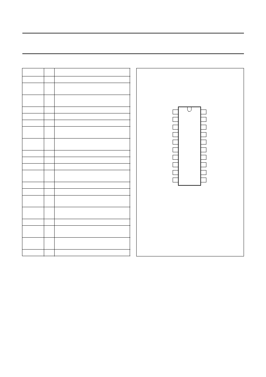
PINNING
SYMBOL PIN
DESCRIPTION
V
DDD
1
digital supply voltage
INM1
2
main divider positive input; rising edge
active
INM2
3
main divider negative input; falling
edge active
DATA
4
serial data input line
CLOCK
5
serial clock input line
STROBE
6
serial strobe input line
INR
7
reference divider input line; rising edge
active
INA
8
auxiliary divider input line; rising edge
active
RA
9
auxiliary current setting; resistor to V
SS
PHA
10
auxiliary phase detector output
PHI
11
integral phase detector output
V
SSA
12
analog ground; internally connected to
V
SS
PHP
13
proportional phase detector output
V
DDA
14
analog supply voltage
RN
15
main current setting input; resistor to
V
SS
RF
16
fractional compensation current setting
input; resistor to V
SS
LOCK
17
lock detector output
FB1
18
feedback output 1 for prescaler
modulus control
FB2
19
feedback output 2 for prescaler
modulus control
V
SS
20
common ground connection
Fig.2 Pin configuration.
1/2 page (Datasheet)
22 mm
1
2
3
4
5
6
7
8
9
10
20
19
18
17
16
15
14
13
12
11
UMA1005T
INM1
INM2
DATA
CLOCK
STROBE
INR
INA
RA
PHA
FB2
FB1
LOCK
RN
PHP
PHI
V DDA
V SSA
MEA667
RF
VDDD
V SS

November 1994
5
Philips Semiconductors
Preliminary specification
Dual low-power frequency synthesizer
UMA1005T
FUNCTIONAL DESCRIPTION
Serial programming input
The serial input is a 3-wire input (CLOCK, STROBE and
DATA) to program all counter ratios, DACs, selection and
enable bits. The programming data is structured into
24 or 32-bit words. Each word includes 1 or 4 address
bits. Figure 3 shows the timing diagram of the serial input.
When the STROBE = LOW, the clock driver is enabled
and on the positive edges of the CLOCK the signal on the
DATA input is clocked into a shift register. When the
STROBE = HIGH, the clock is disabled and the data in the
shift register remains stable. Depending on the
1 or 4 address bits the data is latched into different
working registers or temporary registers. In order to fully
program the synthesizer, 4 words must be sent:
1. D word.
2. C word.
3. B word.
4. A word.
Figure 4 shows the format and the contents of each word.
The E word is for testing purposes only. The E (test) word
is reset when programming the D word. The data for NM4,
CN and PR is stored by the B word temporary registers.
When the A word is loaded, the data of these temporary
registers is loaded together with the A word into the work
registers which avoids false temporary main divider input.
CN is only loaded from the temporary registers when a
short 24-bit A0 word is used. CN will be directly loaded by
programming a long 32-bit A1 word. The flag LONG in the
D word determines whether A0 (LONG = 0) or A1
(LONG = 1) format is applicable.
The A word contains new data for the main divider. The
A word is loaded only when a main divider synchronization
signal is also active, to avoid phase jumps when
reprogramming the main divider. The synchronization
signal is generated by the main divider. It disables the
loading of the A word each main divider cycle during
maximum 300 main divider input cycles. To make sure
that the A word will be correctly loaded the STROBE signal
must be HIGH for at least 300 main divider input cycles.
Programming the A word also means that the main charge
pumps on outputs PHP and PHI are set into the speed-up
mode as long as the STROBE remains HIGH.
Fig.3 Serial input timing sequence.
handbook, full pagewidth
MBE121
data
valid
data
change
t suDA
t hDA
DATA
CLOCK
t HC
t LC
V H
V L
V H
V L
D0
D1
D30
D31
V H
V L
t hST
t suST
clock disabled
store data
clock enabled
shift in data
STROBE

November 1994
6
Philips Semiconductors
Preliminary specification
Dual low-power frequency synthesizer
UMA1005T
Fig.4 Serial input word format.
andbook, full pagewidth
MBE122
NM3
NM2
NM2
CN
0
NF
NM1
word
D31
MSB
A1
LSB
NM3
NM2
NM2
0
NF
NM1
D23
D0
D0
A0
PR = `01'
PR `01'
B
1
NM4
CN
C
0
0
0
CK
CL
PR
1
NR
D
0
1
0
SM
SA
F
1
NA
0
0
1
PA
0
0
0
0
0
0
EM
EA M
O
D
L
O
N
G
1
E
1
1
1
D0
D23
TEST BITS
address bits

November 1994
7
Philips Semiconductors
Preliminary specification
Dual low-power frequency synthesizer
UMA1005T
Table 1
Description of symbols used in Fig.4
Notes
1. X = don't care.
2. Not including reset cycles and fractional-N effects.
SYMBOL
BITS
(1)
FUNCTION
NM1
12
number of main divider cycles when prescaler is programmed in ratio
R1 (FB1 = 1; FB2 = 0); note 2
NM2
8 if PR = 01
number of main divider cycles when prescaler is programmed in ratio
R2 (FB1 = 0; FB2 = 0); note 2
4 if PR
01
NM3
4 if PR = 1X
number of main divider cycles when prescaler is programmed in ratio
R3 (FB1 = 0; FB2 = 1); note 2
NM4
4 if PR = 11 or 00
number of main divider cycles when prescaler is programmed in ratio
R4 (FB1 = 1; FB2 = 1); note 2
PR
2
prescaler type in use:
PR = 01; modulus 2 prescaler
PR = 10; modulus 3 prescaler
PR = 11; modulus 4 prescaler
PR = 00; modulus 4 prescaler (inhibit ratio 3)
NF
3
fractional-N increment
FMOD
1
fraction-N modulus selection flag:
1 = modulo 8
0 = modulo 5
LONG
1
A word format selection flag:
0 = 24-bit A0 format
1 = 32-bit A1 format
CN
8
binary current setting factor for main charge pumps
CL
2
binary acceleration factor for proportional charge pump current
CK
4
binary acceleration factor for integral charge pump current
EM
1
main divider enable flag
EA
1
auxiliary divider enable flag
SM
2
reference select for main phase detector
SA
2
reference select for auxiliary phase detector
NR
9
reference divider ratio
NA
9
auxiliary divider ratio
PA
1
auxiliary prescaler mode:
PA = 0; divide-by-4
PA = 1; divide-by-1
Auxiliary variable divider
The input signal on INA is amplified to a logic level by a
single ended input buffer, which accepts LOW level AC
coupled input signals. This input stage is enabled if the
serial control bit EA = 1. Disabling means that all currents
in the input stage are switched off. A fixed divide by 4 is
enabled if PA = 0. This divider has been optimized to
accept a high-frequency (90 MHz at a supply voltage
range of 4.75 to 5.5 V) input signal. If PA = 1 this divider is
disabled and the input signal is fed directly to the second

November 1994
8
Philips Semiconductors
Preliminary specification
Dual low-power frequency synthesizer
UMA1005T
stage, which is a 9-bit programmable divider with standard
input frequency (30 MHz). The division ratio can be
expressed as:
If PA = 0; N = 4
◊
NA.
If PA = 1; N = NA; with NA = 4 to 511.
Reference variable divider (Fig.5)
The input signal on INR is amplified to a logic level by a
single ended input buffer, which accepts LOW level AC
coupled input signals. This input stage is enabled by the
OR function of the serial input bits EA and EM. Disabling
means that all currents in the input stage are switched off.
The reference divider consists of a programmable divider
by NR (NR = 4 to 511) followed by a 3-bit binary counter.
The 2-bit SM determines which of the 4 output pulses is
selected as main phase detector input. The 2-bit SA
determines the selection of the auxiliary phase detector
signal. To obtain the best time spacing for the main and
auxiliary reference signals, the opposite output will be
used for the auxiliary phase detector, reducing the
possibility of unwanted interactions. For this reason the
programmable divider produces a symmetric output pulse
for even ratios and a 1 input cycle asymmetric pulse for
odd ratios.
Main variable divider
The input signals on INM1 and INM2 are amplified to a
logic level by a balanced input comparator giving a
common mode rejection. This input stage is enabled when
serial control bit EM = 1. Disabling means that all currents
in the comparator are switched off. The main divider is
built-up by a 12-bit counter plus a sign bit. Depending on
the serial input values of NM1, NM2, NM3, NM4 and the
prescaler select PR, the counter will select a prescaler
ratio during a number of input cycles in accordance with
the information in Table 2.
Fig.5 Reference variable divider.
book, full pagewidth
MBE123
divide by NR
reference
input
2
2
2
MAIN SELECT
SM = `00'
SM = `01'
SM = `10'
SM = `11'
main
phase
detector
AUXILIARY SELECT
SA = `11'
SA = `10'
SA = `01'
SA = `00'
auxiliary
phase
detector

November 1994
9
Philips Semiconductors
Preliminary specification
Dual low-power frequency synthesizer
UMA1005T
Table 2
Selection of prescaler ratio
Notes
1. X = don't care.
2. When the fractional accumulator overflows.
The total division ratio from prescaler to the phase detector expressions are given in Table 3.
Table 3
Total division from prescaler to phase detector expressions
Note
1. When the fractional accumulator overflows.
When the prescaler ratio is R2 = R1 + 1 the total division ratio N
= N + 1.
Table 4
Modulus prescaler
COUNTER
STATUS
FB1
FB2
PRESCALER RATIO
(1)
(
-
NM1
-
1) to 0
1
0
R1
(
-
NM1
-
1) to
-
1
1
0
R1
(2)
1 to NM2
0
0
R2
0 to NM2
0
0
R2
(2)
0 to NM3
0
1
R3; if PR = 1X
0 to NM4
1
1
R4; if PR = 11 or 00
CONDITION
EXPRESSION
PR = 01
N = (NM1 + 2)
◊
R1 + NM2
◊
R2
N
= (NM1 + 1)
◊
R1 + (NM2 + 1)
◊
R2; note 1
PR = 10
N = (NM1 + 2)
◊
R1 + NM2
◊
R2 + (NM3 + 1)
◊
R3
N
= (NM1 + 1)
◊
R1 + (NM2 + 1)
◊
R2 + (NM3 + 1)
◊
R3; note 1
PR = 11
N = (NM1 + 2)
◊
R1 + NM2
◊
R2 + (NM3 + 1)
◊
R3 + (NM4 + 1)
◊
R4
N
= (NM1 + 1)
◊
R1 + (NM2 + 1)
◊
R2 + (NM3 + 1)
◊
R3 + (NM4 + 1)
◊
R4; note 1
PR = 00
N = (NM1 + 2)
◊
R1 + NM2
◊
R2 + (NM4 + 1)
◊
R4
N
= (NM1 + 1)
◊
R1 + (NM2 + 1)
◊
R2 + (NM4 + 1)
◊
R4; note 1
PR
MODULUS PRESCALER
BIT CAPACITY
NM1
NM2
NM3
NM4
00
4
12
4
-
4
01
2
12
8
-
-
10
3
12
4
4
-
11
4
12
4
4
4

November 1994
10
Philips Semiconductors
Preliminary specification
Dual low-power frequency synthesizer
UMA1005T
The loading of the work registers NM1, NM2, NM3, NM4
and PR is synchronized with the state of the main counter,
to avoid extra phase disturbance when switching over to
another main divider ratio as is explained in Section "Serial
programming input".
At the completion of a main divider cycle, a main divider
output pulse is generated which will drive the main phase
comparator. Also the fractional accumulator is
incremented with NF. The accumulator works modulo Q.
Q is preset by the serial control bit FMOD to 8 when
FMOD = 1. Each time the accumulator overflows, the
feedback to the prescaler will select one cycle using
prescaler ratio R2 instead of R1.
As shown above, this will increase the overall division ratio
by 1 if R2 = R1 + 1. The mean division ratio over Q main
divider cycles will then be:
Programming a fraction means the prescaler with main
divider will divide by N or N + 1.
The output of the main divider will be modulated with a
fractional phase ripple. This phase ripple is proportional to
the contents of the fractional accumulator FRD, which is
used for fractional current compensation.
Phase detectors (Fig.6)
The auxiliary and main phase detectors are a 2 D-type
flip-flop phase and frequency detector. The flip-flops are
set by the negative edges of output signals of the dividers.
The reset inputs are activated when both flip-flops have
been set and when the reset enable signal is active (LOW).
Around zero phase error this has the effect of delaying the
reset for 1 reference input cycle. This avoids non-linearity
or dead band around zero phase error. The flip-flops drive
on-chip charge pumps. A pull-up current from the charge
pump indicates that the VCO frequency shall be increased
while a pull-down pulse indicates that the VCO frequency
shall be decreased.
Current settings
The UMA1005T has 3 current setting pins RA, RN and RF.
The active charge pump currents and the fractional
compensation currents are linearly dependent on the
current in the current setting pins. This current I
R
can be
set by an external resistor to be connected between the
current setting pin (pin 9) and V
SS
. The typical value for R
(current setting resistor) can be calculated with the
NQ
N
NF
Q
--------
+
=
equation:
The current can be set to zero by connecting the
corresponding pin to V
DDA
.
Auxiliary output charge pumps
The auxiliary charge pumps on pin PHA are driven by the
auxiliary phase detector and the current value is
determined by the external resistor (R
ext
) at pin RA. The
active charge pump current is typically: |I
PHA
| = 8
◊
I
RA
.
Main output charge pumps and fractional
compensation currents
The main charge pumps on pins PHP and PHI are driven
by the main phase detector and the current value is
determined by the current at pin RN and via a number of
DACs which are driven by registers of the serial input. The
fractional compensation current is determined by the
current at pin RF, the contents of the fractional
accumulator FRD and a number of DACs driven by
registers from the serial input. The timing for the fractional
compensation is derived from the reference divider. The
current is on during 1 input reference cycle before and
1 cycle after the output signal to the phase comparator.
Figure 7 shows the waveforms for a typical case.
When the serial input A word is loaded, the output circuits
are in the `speed-up mode' as long as the STROBE is
HIGH, else the `normal mode' is active.
N
ORMAL MODE
In the `normal mode' the current output at PHP is:
I
PHP(N)
= I
pump10
+ I
comp10
.
Where:
; charge pump current.
; fractional compensation current.
In `normal mode' the current at output PHI is zero.
R
V
DDA
0.5
≠
(
)
237 I
R
≠
I
R
-------------------------------------------------------------
=
I
pump10
CN
I
RN
◊
29
------------------------
=
I
comp10
FRD
I
RF
◊
128
---------------------------
=

November 1994
11
Philips Semiconductors
Preliminary specification
Dual low-power frequency synthesizer
UMA1005T
handbook, full pagewidth
MBE124
INR
L
R
X
P
N
PH
AUXILIARY
AND MAIN
DIVIDER
R
D
C
Q
R
D
C
Q
`1'
X
`1'
R
L
REFERENCE
DIVIDER
INR
VSSA
VDDA
P
N
P-type
charge pump
N-type
charge pump
PH
Fig.6 Phase detector structure with timing.

November 1994
12
Philips Semiconductors
Preliminary specification
Dual low-power frequency synthesizer
UMA1005T
S
PEED
-
UP MODE
In `speed-up mode' the current in output PHP is:
I
PHP(S)
= I
PHP(N)
+ I
pump11
+ I
comp11
.
Where:
I
pump11
= I
pump10
◊
2
(CL + 1)
; charge pump current.
I
comp11
= I
comp10
◊
2
(CL + 1)
; fractional compensation
current.
In `speed-up mode' the current in output PHI is:
I
PHI(S)
= I
pump21
+ I
comp21
.
Where:
I
pump21
= I
pump11
◊
CK; charge pump current.
I
comp21
= I
comp11
◊
CK; fractional compensation current.
Figure 7 shows that for a proper fractional compensation
the area of the fractional compensation current pulse must
be equal to the area of the charge pump ripple output. This
means that the current setting on the inputs RN and RF
must have following ratio:
.
Where:
Q = fractional-N modulus.
f
VCO
= f
i(max)1
◊
N; input frequency of the prescaler.
f
i(max)1
= maximum input frequency of the main divider
(pins INM1 and INM2).
f
i(max)2
= maximum input frequency of the reference
divider (pin INR).
Lock detect
The output LOCK is HIGH when the auxiliary phase
detector and the main phase detector indicate a lock
condition. The lock condition is defined as a phase
difference of less than
±
1 cycle on the reference input INR.
The lock condition is also fulfilled when the relative counter
is disabled (EM = 0 or EA = 0 respectively) for the main or
auxiliary counter respectively.
I
RN
I
RF
--------
29
Q
◊
f
VCO
◊
64
CN
◊
f
i max
(
)
2
◊
------------------------------------------------
=

November 1994
13
Philips Semiconductors
Preliminary specification
Dual low-power frequency synthesizer
UMA1005T
handbook, full pagewidth
MBE125
INR
INM
N
N
N
1
N
N
1
detector output
contents
accumulator
2
4
1
3
0
fractional
compensation
current
pulse-width
modulation
mA
µ
A
t 1
t 2
pulse-level
modulation
outputs
PHP and PHI
Fig.7 Waveforms for NF = 2 and fraction = 0.4.

November 1994
14
Philips Semiconductors
Preliminary specification
Dual low-power frequency synthesizer
UMA1005T
LIMITING VALUES
In accordance with the Absolute Maximum Rating System (IEC 134).
DC CHARACTERISTICS
V
DDD
= V
DDA
= 2.9 to 5.5 V; T
amb
=
-
40 to +70
∞
C; unless otherwise specified.
SYMBOL
PARAMETER
MIN.
MAX.
UNIT
V
DDD
digital supply voltage
-
0.5
6.5
V
V
DDA
analog supply voltage
-
0.5
6.5
V
V
I
voltage on any input
-
0.5
V
DD
+ 0.5 V
I
n
DC current into any input or output
-
10
+10
mA
P
tot
total power dissipation
-
25
mW
T
stg
storage temperature
-
65
+150
∞
C
T
amb
operating ambient temperature
-
40
+70
∞
C
SYMBOL
PARAMETER
CONDITIONS
MIN.
TYP.
MAX.
UNIT
Supply
I
DDD(stb)
digital standby supply
current
EM = EA = 0; inputs on
V
DD
or 0
-
-
5
µ
A
I
DDD
operating digital supply
current
note 1
-
-
5
mA
I
DDA(stb)
analog standby supply
current
V
RA
= V
DDA
; V
RF
= V
DDA
;
V
RN
= V
DDA
-
-
10
µ
A
I
DDA
operating analog supply
current
note 1
-
-
0.6
mA
Digital inputs CLK, DATA and STROBE
V
IH
HIGH level input voltage
0.7V
DD
-
V
DD
V
V
IL
LOW level input voltage
0
-
0.3V
DD
V
Digital outputs FB1, FB2 and LOCK
V
OL
LOW level output voltage
I
O
= 2 mA; note 2
-
-
0.4
V
V
OH
HIGH level output voltage
I
O
=
-
2 mA; note 2
V
DD
-
0.4
-
-
V
Charge pump PHA
I
PHA
output current
I
RA
=
-
62.5
µ
A;
V
PHA
=
1
/
2
V
DD
; note 2
400
500
600
µ
A
I
RA
=
-
25
µ
A; V
PHA
=
1
/
2
V
DD
160
200
240
µ
A
relative output current
variation
I
RA
=
-
62.5
µ
A;
notes 2 and 3
-
2
6
%
I
PHA M
output current matching
I
RA
=
-
62.5
µ
A;
V
PHA
=
1
/
2
V
DD
;
notes 2 and 4
-
-
±
50
µ
A
I
PHA
I
PHA
---------------

November 1994
15
Philips Semiconductors
Preliminary specification
Dual low-power frequency synthesizer
UMA1005T
Charge pump PHP; normal mode (notes 5, 6 and 7); V
RF
= V
DD
I
PHP(N)
output current
I
RN
=
-
62.5
µ
A;
V
PHP
=
1
/
2
V
DD
; note 2
440
550
660
µ
A
I
RN
=
-
25
µ
A; V
PHP
=
1
/
2
V
DD
175
220
265
µ
A
I
PHP(N)
relative output current
variation
I
RN
=
-
62.5
µ
A; note 3
-
2
6
%
I
PHP(N M)
output current matching
I
RN
=
-
62.5
µ
A;
V
PHP
=
1
/
2
V
DD
;
notes 2 and 4
-
-
±
50
µ
A
Charge pump PHP; speed-up mode (notes 5, 6 and 8); V
RF
= V
DD
I
PHP(S)
output current
I
RN
=
-
62.5
µ
A;
V
PHP
=
1
/
2
V
DD
; note 2
2.20
2.75
3.30
mA
I
RN
=
-
25
µ
A; V
PHP
=
1
/
2
V
DD
0.85
1.1
1.35
mA
I
PHP(S)
relative output current
variation
I
RN
=
-
62.5
µ
A;
notes 2 and 3
-
2
6
%
I
PHP(S M)
output current matching
I
RN
=
-
62.5
µ
A;
V
PHP
=
1
/
2
V
DD
;
notes 2 and 4
-
-
±
250
µ
A
Charge pump PHI; speed-up mode (notes 5, 6 and 9); V
RF
= V
DD
I
PHI(S)
output current
I
RN
=
-
62.5
µ
A;
V
PHI
=
1
/
2
V
DD
; note 2
4.4
5.5
6.6
mA
I
RN
=
-
25
µ
A; V
PHI
=
1
/
2
V
DD
1.75
2.2
2.65
mA
I
PHI(S)
relative output current
variation
I
RN
=
-
62.5
µ
A;
notes 2 and 3
-
2
8
%
I
PHI(S M)
output current matching
I
RN
=
-
62.5
µ
A;
V
PHI
=
1
/
2
V
DD
; notes 2 and 4
-
-
±
500
µ
A
Fractional compensation PHP; normal mode (notes 5, 10 and 11); V
RN
= V
DD
; V
PHP
=
1
/
2
V
DD
I
PHP(F N)
fractional compensation
output current PHP as a
function of FRD
I
RF
=
-
62.5
µ
A;
FRD = 1 to 7;
notes 2 and 12
-
675
-
500
-
325
nA
I
RF
=
-
25
µ
A; FRD = 1 to 7;
note 12
-
270
-
200
-
130
nA
Fractional compensation PHP; speed-up mode (notes 5, 11 and 13); V
RN
= V
DD
; V
PHP
=
1
/
2
V
DD
I
PHP(F S)
fractional compensation
output current PHP as a
function of FRD
I
RN
=
-
62.5
µ
A;
FRD = 1 to 7;
notes 2 and 12
-
3.35
-
2.50
-
1.65
µ
A
I
RN
=
-
25
µ
A; FRD = 1 to 7;
note 12
-
1.35
-
1.00
-
0.65
µ
A
SYMBOL
PARAMETER
CONDITIONS
MIN.
TYP.
MAX.
UNIT

November 1994
16
Philips Semiconductors
Preliminary specification
Dual low-power frequency synthesizer
UMA1005T
Notes
1. Operational conditions:
a) Main and auxiliary divider enabled (EM = EA = 1).
b) NA = 125.
c) NR = 125.
d) NM1 = 60.
e) NM2 = 63.
f) f
i(max)1
= f
i(max)2
= 15 MHz.
g) f
i(max)3
= 60 MHz.
h) Lock condition.
i)
Normal mode; note 5
j)
I
RN
= I
RF
= I
RA
= 25
µ
A.
k) CN = 255.
l)
PA = 0.
2. Limited supply voltage range 4.5 to 5.5 V.
3. The relative output current variation is defined as:
; with V
1
= 0.7 V; V
2
= V
DD
-
0.8 V (see Fig.8).
4. The output current matching is measured when both (positive and negative current) sections of the output charge
pumps are on.
5. When a serial `A' word is programmed, the main charge pumps on PHP and PHI are in the `speed-up mode' as long
as STROBE = HIGH, otherwise the main charge pumps are in the `normal mode'.
6. Monotonicity is guaranteed with CN = 0 to 255.
7. Typical output current:
; specification condition: CN = 255.
Fractional compensation PHI; speed-up mode (notes 5, 11 and 14); V
RN
= V
DD
; V
PHP
=
1
/
2
V
DD
I
PHI(F)
fractional compensation
output current PHI as a
function of FRD
I
RN
=
-
62.5
µ
A;
FRD = 1 to 7;
notes 2 and 12
-
5.4
-
4.0
-
2.6
µ
A
I
RN
=
-
25
µ
A; FRD = 1 to 7;
note 12
-
2.15
-
1.60
-
1.05
µ
A
Charge pump leakage currents; charge pump not active
I
PHP(LO)
output leakage current PHP normal mode;
V
PHP
= 0.7 to V
DDA
-
0.8 V
note 5
-
10
750
nA
I
PHI(LO)
output leakage current PHI
normal mode;
V
PHI
= 0.7 to V
DDA
-
0.8 V
note 5
-
10
100
nA
I
PHA(LO)
output leakage current PHA V
PHA
= 0.7 to V
DDA
-
0.8 V
-
10
750
nA
SYMBOL
PARAMETER
CONDITIONS
MIN.
TYP.
MAX.
UNIT
I
O
I
O
---------
2
I
2
I
1
≠
I
2
I
1
+
------------------
◊
=
I
PHP(N)
I
RN
≠
CN
29
---------
◊
=

November 1994
17
Philips Semiconductors
Preliminary specification
Dual low-power frequency synthesizer
UMA1005T
8. Typical output current:
; specification conditions:
a) CN = 255; CL = 1 or,
b) CN = 75; CL = 3.
9. Typical output current:
; specification conditions:
a) CN = 160; CL = 3; CK = 1 or,
b) CN = 160; CL = 2; CK = 2 or,
c) CN = 160; CL = 1; CK = 4 or,
d) CN = 160; CL = 0; CK = 8.
10. Typical fractional compensation output current:
; specification condition: FRD = 1 to 7.
11. The compensation current specified does not include the leakage current of this output.
12. FRD is the value of the 3-bit fractional accumulator.
13. Typical fractional compensation output current:
; specification conditions:
FRD = 1 to 7; CL = 1.
14. Typical fractional compensation output current:
; specification conditions:
a) FRD = 1 to 7; CL = 1; CK = 2 or,
b) FRD = 1 to 7; CL = 2; CK = 1.
I
PHP(S)
I
RN
≠
CN
2
CL
1
+
(
)
1
+
29
-------------------------------
◊
◊
=
I
PHI
I
RN
≠
CN
◊
2
CL
1
+
(
)
CK
29
--------
◊
◊
=
I
PHP(F N)
I
RF
FRD
128
-------------
◊
=
I
PHP(F S)
I
RF
FRD
◊
2
CL
1
+
(
)
1
+
128
-------------------------------
◊
=
I
PHI(F)
I
RF
FRD
◊
2
CL
1
+
(
)
◊
CK
128
----------
◊
=

November 1994
18
Philips Semiconductors
Preliminary specification
Dual low-power frequency synthesizer
UMA1005T
AC CHARACTERISTICS
V
DDD
= V
DDA
= 2.9 to 5.5 V; T
amb
=
-
40 to +70
∞
C; unless otherwise specified.
SYMBOL
PARAMETER
CONDITIONS
MIN.
TYP.
MAX.
UNIT
Main divider (inputs INM1 and INM2)
f
i(max)1
maximum input frequency
10
-
-
MHz
note 1
30
-
-
MHz
V
INM(p-p)
differential input signal
amplitude V
INM1
-
V
INM2
(peak-to-peak value)
600
-
-
mV
V
CM
common mode range for
V
INM1
and V
INM2
1
-
V
DD
-
1
V
t
pd
propagation delay time
from I
NM1
and I
NM2
to FB1
and FB2
-
-
60
ns
note 1
-
18
30
ns
msr
mark-to-space ratio for
differential input signals
35 : 65
-
65 : 35
Z
i(min)
minimum input impedance
resistive; note 2
5
-
-
k
capacitive; note 2
-
-
5
pF
Fig.8 Relative output current variation.
handbook, full pagewidth
MBE126
I 2
I
I
1
I 2
I 1
V1
V
V
2
o
o
November 1994
19
Philips Semiconductors
Preliminary specification
Dual low-power frequency synthesizer
UMA1005T
Notes
1. Limited supply voltage range 4.5 to 5.5 V.
2. Periodically sampled; not 100% tested.
Reference divider (input INR)
f
i(max)2
maximum input frequency
15
-
-
MHz
note 1
30
-
-
MHz
V
i(p-p)
input signal amplitude
AC coupled (peak-to-peak
value)
300
-
-
mV
Z
i(min)
minimum input impedance
resistive; note 2
5
-
-
k
capacitive; note 2
-
-
5
pF
Auxiliary divider (input INA)
f
i(max)3
maximum input frequency
prescaler enabled; PA = 0
35
-
-
MHz
prescaler enabled; PA = 0;
note 1
90
-
-
MHz
prescaler disabled; PA = 1
15
-
-
MHz
prescaler disabled; PA = 1;
note 1
30
-
-
MHz
V
i(p-p)
input signal amplitude AC
coupled (peak-to-peak
value)
300
-
-
mV
Z
i(min)
minimum input impedance
resistive; note 2
5
-
-
k
capacitive; note 2
-
-
5
pF
Serial interface (inputs DATA, CLOCK and STROBE); see Fig.3
f
clk
clock frequency
-
-
10
MHz
t
HC
clock HIGH time
30
-
-
ns
t
LC
clock LOW time
30
-
-
ns
t
suDA
DATA set-up time
30
-
-
ns
t
hDA
DATA hold time
30
-
-
ns
t
suST
STROBE set-up time
30
-
-
ns
t
hST
STROBE hold time
30
-
-
ns
SYMBOL
PARAMETER
CONDITIONS
MIN.
TYP.
MAX.
UNIT

November 1994
20
Philips Semiconductors
Preliminary specification
Dual low-power frequency synthesizer
UMA1005T
PACKAGE OUTLINE
handbook, full pagewidth
A
MBC237 - 1
0.15
0
1.4
1.2
0.8
0.3
0.20
0.13
0.6
0.5
0 to 10
o
1.5
1.2
detail A
S
6.75
6.40
0.1 S
pin 1
index
0.6
0.2
(4x)
0.13 M
(20x)
0.32
0.20
0.65
4.5
4.3
6.6
6.2
1
10
20
11
Fig.9 Plastic shrink small outline package; 20 leads; body width 4.4 mm (SSOP20; SOT266-1).
Dimensions in mm.

November 1994
21
Philips Semiconductors
Preliminary specification
Dual low-power frequency synthesizer
UMA1005T
SOLDERING
Plastic small-outline packages
B
Y WAVE
During placement and before soldering, the component
must be fixed with a droplet of adhesive. After curing the
adhesive, the component can be soldered. The adhesive
can be applied by screen printing, pin transfer or syringe
dispensing.
Maximum permissible solder temperature is 260
∞
C, and
maximum duration of package immersion in solder bath is
10 s, if allowed to cool to less than 150
∞
C within 6 s.
Typical dwell time is 4 s at 250
∞
C.
A modified wave soldering technique is recommended
using two solder waves (dual-wave), in which a turbulent
wave with high upward pressure is followed by a smooth
laminar wave. Using a mildly-activated flux eliminates the
need for removal of corrosive residues in most
applications.
B
Y SOLDER PASTE REFLOW
Reflow soldering requires the solder paste (a suspension
of fine solder particles, flux and binding agent) to be
applied to the substrate by screen printing, stencilling or
pressure-syringe dispensing before device placement.
Several techniques exist for reflowing; for example,
thermal conduction by heated belt, infrared, and
vapour-phase reflow. Dwell times vary between 50 and
300 s according to method. Typical reflow temperatures
range from 215 to 250
∞
C.
Preheating is necessary to dry the paste and evaporate
the binding agent. Preheating duration: 45 min at 45
∞
C.
R
EPAIRING SOLDERED JOINTS
(
BY HAND
-
HELD SOLDERING
IRON OR PULSE
-
HEATED SOLDER TOOL
)
Fix the component by first soldering two, diagonally
opposite, end pins. Apply the heating tool to the flat part of
the pin only. Contact time must be limited to 10 s at up to
300
∞
C. When using proper tools, all other pins can be
soldered in one operation within 2 to 5 s at between 270
and 320
∞
C. (Pulse-heated soldering is not recommended
for SO packages.)
For pulse-heated solder tool (resistance) soldering of VSO
packages, solder is applied to the substrate by dipping or
by an extra thick tin/lead plating before package
placement.
DEFINITIONS
LIFE SUPPORT APPLICATIONS
These products are not designed for use in life support appliances, devices, or systems where malfunction of these
products can reasonably be expected to result in personal injury. Philips customers using or selling these products for
use in such applications do so at their own risk and agree to fully indemnify Philips for any damages resulting from such
improper use or sale.
Data sheet status
Objective specification
This data sheet contains target or goal specifications for product development.
Preliminary specification
This data sheet contains preliminary data; supplementary data may be published later.
Product specification
This data sheet contains final product specifications.
Limiting values
Limiting values given are in accordance with the Absolute Maximum Rating System (IEC 134). Stress above one or
more of the limiting values may cause permanent damage to the device. These are stress ratings only and operation
of the device at these or at any other conditions above those given in the Characteristics sections of the specification
is not implied. Exposure to limiting values for extended periods may affect device reliability.
Application information
Where application information is given, it is advisory and does not form part of the specification.

November 1994
22
Philips Semiconductors
Preliminary specification
Dual low-power frequency synthesizer
UMA1005T
NOTES

November 1994
23
Philips Semiconductors
Preliminary specification
Dual low-power frequency synthesizer
UMA1005T
NOTES

Philips Semiconductors
Philips Semiconductors ≠ a worldwide company
Argentina: IEROD, Av. Juramento 1992 - 14.b, (1428)
BUENOS AIRES, Tel. (541)786 7633, Fax. (541)786 9367
Australia: 34 Waterloo Road, NORTH RYDE, NSW 2113,
Tel. (02)805 4455, Fax. (02)805 4466
Austria: Triester Str. 64, A-1101 WIEN, P.O. Box 213,
Tel. (01)60 101-1236, Fax. (01)60 101-1211
Belgium: Postbus 90050, 5600 PB EINDHOVEN, The Netherlands,
Tel. (31)40 783 749, Fax. (31)40 788 399
Brazil: Rua do Rocio 220 - 5
th
floor, Suite 51,
CEP: 04552-903-S√O PAULO-SP, Brazil.
P.O. Box 7383 (01064-970).
Tel. (011)821-2333, Fax. (011)829-1849
Canada: PHILIPS SEMICONDUCTORS/COMPONENTS:
Tel. (800) 234-7381, Fax. (708) 296-8556
Chile: Av. Santa Maria 0760, SANTIAGO,
Tel. (02)773 816, Fax. (02)777 6730
Colombia: IPRELENSO LTDA, Carrera 21 No. 56-17,
77621 BOGOTA, Tel. (571)249 7624/(571)217 4609,
Fax. (571)217 4549
Denmark: Prags Boulevard 80, PB 1919, DK-2300 COPENHAGEN S,
Tel. (032)88 2636, Fax. (031)57 1949
Finland: Sinikalliontie 3, FIN-02630 ESPOO,
Tel. (9)0-50261, Fax. (9)0-520971
France: 4 Rue du Port-aux-Vins, BP317,
92156 SURESNES Cedex,
Tel. (01)4099 6161, Fax. (01)4099 6427
Germany: P.O. Box 10 63 23, 20043 HAMBURG,
Tel. (040)3296-0, Fax. (040)3296 213.
Greece: No. 15, 25th March Street, GR 17778 TAVROS,
Tel. (01)4894 339/4894 911, Fax. (01)4814 240
Hong Kong: PHILIPS HONG KONG Ltd., 6/F Philips Ind. Bldg.,
24-28 Kung Yip St., KWAI CHUNG, N.T.,
Tel. (852)424 5121, Fax. (852)428 6729
India: Philips INDIA Ltd, Shivsagar Estate, A Block ,
Dr. Annie Besant Rd. Worli, Bombay 400 018
Tel. (022)4938 541, Fax. (022)4938 722
Indonesia: Philips House, Jalan H.R. Rasuna Said Kav. 3-4,
P.O. Box 4252, JAKARTA 12950,
Tel. (021)5201 122, Fax. (021)5205 189
Ireland: Newstead, Clonskeagh, DUBLIN 14,
Tel. (01)640 000, Fax. (01)640 200
Italy: PHILIPS SEMICONDUCTORS S.r.l.,
Piazza IV Novembre 3, 20124 MILANO,
Tel. (0039)2 6752 2531, Fax. (0039)2 6752 2557
Japan: Philips Bldg 13-37, Kohnan 2 -chome, Minato-ku, TOKYO 108,
Tel. (03)3740 5028, Fax. (03)3740 0580
Korea: (Republic of) Philips House, 260-199 Itaewon-dong,
Yongsan-ku, SEOUL, Tel. (02)794-5011, Fax. (02)798-8022
Malaysia: No. 76 Jalan Universiti, 46200 PETALING JAYA,
SELANGOR, Tel. (03)750 5214, Fax. (03)757 4880
Mexico: 5900 Gateway East, Suite 200, EL PASO, TX 79905,
Tel. 9-5(800)234-7381, Fax. (708)296-8556
Netherlands: Postbus 90050, 5600 PB EINDHOVEN, Bldg. VB
Tel. (040)783749, Fax. (040)788399
New Zealand: 2 Wagener Place, C.P.O. Box 1041, AUCKLAND,
Tel. (09)849-4160, Fax. (09)849-7811
Norway: Box 1, Manglerud 0612, OSLO,
Tel. (022)74 8000, Fax. (022)74 8341
Pakistan: Philips Electrical Industries of Pakistan Ltd.,
Exchange Bldg. ST-2/A, Block 9, KDA Scheme 5, Clifton,
KARACHI 75600, Tel. (021)587 4641-49,
Fax. (021)577035/5874546.
Philippines: PHILIPS SEMICONDUCTORS PHILIPPINES Inc,
106 Valero St. Salcedo Village, P.O. Box 2108 MCC, MAKATI,
Metro MANILA, Tel. (02)810 0161, Fax. (02)817 3474
Portugal: PHILIPS PORTUGUESA, S.A.,
Rua dr. AntÛnio Loureiro Borges 5, Arquiparque - Miraflores,
Apartado 300, 2795 LINDA-A-VELHA,
Tel. (01)4163160/4163333, Fax. (01)4163174/4163366.
Singapore: Lorong 1, Toa Payoh, SINGAPORE 1231,
Tel. (65)350 2000, Fax. (65)251 6500
South Africa: S.A. PHILIPS Pty Ltd.,
195-215 Main Road Martindale, 2092 JOHANNESBURG,
P.O. Box 7430 Johannesburg 2000,
Tel. (011)470-5911, Fax. (011)470-5494.
Spain: Balmes 22, 08007 BARCELONA,
Tel. (03)301 6312, Fax. (03)301 42 43
Sweden: Kottbygatan 7, Akalla. S-164 85 STOCKHOLM,
Tel. (0)8-632 2000, Fax. (0)8-632 2745
Switzerland: Allmendstrasse 140, CH-8027 ZÐRICH,
Tel. (01)488 2211, Fax. (01)481 77 30
Taiwan: PHILIPS TAIWAN Ltd., 23-30F, 66, Chung Hsiao West
Road, Sec. 1. Taipeh, Taiwan ROC, P.O. Box 22978,
TAIPEI 100, Tel. (02)388 7666, Fax. (02)382 4382.
Thailand: PHILIPS ELECTRONICS (THAILAND) Ltd.,
209/2 Sanpavuth-Bangna Road Prakanong,
Bangkok 10260, THAILAND,
Tel. (662)398-0141, Fax. (662)398-3319.
Turkey: Talatpasa Cad. No. 5, 80640 GÐLTEPE/ISTANBUL,
Tel. (0 212)279 2770, Fax. (0212)269 3094
United Kingdom: Philips Semiconductors LTD.,
276 Bath road, Hayes, MIDDLESEX UB3 5BX,
Tel. (081)73050000, Fax. (081)7548421
United States: 811 East Arques Avenue, SUNNYVALE,
CA 94088-3409, Tel. (800)234-7381, Fax. (708)296-8556
Uruguay: Coronel Mora 433, MONTEVIDEO,
Tel. (02)70-4044, Fax. (02)92 0601
For all other countries apply to: Philips Semiconductors,
International Marketing and Sales, Building BE-p,
P.O. Box 218, 5600 MD, EINDHOVEN, The Netherlands,
Telex 35000 phtcnl, Fax. +31-40-724825
SCD35
© Philips Electronics N.V. 1994
All rights are reserved. Reproduction in whole or in part is prohibited without the
prior written consent of the copyright owner.
The information presented in this document does not form part of any quotation
or contract, is believed to be accurate and reliable and may be changed without
notice. No liability will be accepted by the publisher for any consequence of its
use. Publication thereof does not convey nor imply any license under patent- or
other industrial or intellectual property rights.
Printed in The Netherlands
413061/1500/02/pp24
Date of release: November 1994
Document order number:
9397 743 40011