 | –≠–ª–µ–∫—Ç—Ä–æ–Ω–Ω—ã–π –∫–æ–º–ø–æ–Ω–µ–Ω—Ç: UMA1021AM | –°–∫–∞—á–∞—Ç—å:  PDF PDF  ZIP ZIP |

DATA SHEET
Product specification
Supersedes data of 1998 Mar 03
File under Integrated Circuits, IC17
1998 Nov 19
INTEGRATED CIRCUITS
UMA1021AM
Low-voltage frequency synthesizer
for radio telephones
1998 Nov 19
2
Philips Semiconductors
Product specification
Low-voltage frequency synthesizer for
radio telephones
UMA1021AM
FEATURES
∑
Low phase noise
∑
Low current from 3 V supply
∑
Fully programmable main divider
∑
3-line serial interface bus
∑
Independent fully programmable reference divider,
driven from external crystal oscillator
∑
Hard and soft power-down control.
APPLICATIONS
∑
900 MHz and 2 GHz mobile telephones
∑
Portable battery-powered radio equipment.
GENERAL DESCRIPTION
The UMA1021AM BICMOS device integrates a prescaler,
programmable dividers, and a phase comparator to
implement a phase-locked loop.
The device is designed to operate from 3 NiCd cells, in
pocket phones, with low current and nominal 3 V supplies.
The synthesizer operates at RF input frequencies
up to 2.2 GHz with a fully programmable reference divider.
All divider ratios are supplied via a 3-wire serial
programming bus.
Separate power and ground pins are provided to the
analog (charge pump) and digital circuits. The ground
leads should be externally short-circuited to prevent large
currents flowing across the die and thus causing damage.
V
DD1
and V
DD2
must also be at the same potential (V
DD
).
V
CC
must be equal to or greater than V
DD
for wider control
range of the Voltage Controlled Oscillator (VCO),
e.g. V
DD
= 3 V and V
CC
= 5 V.
The charge pump current (phase detector gain) is fixed by
an external resistor at pin I
SET
and controlled via the serial
interface. Only a passive loop filter is necessary; the
charge pump functions within a wide voltage compliance
range to improve the overall system performance.
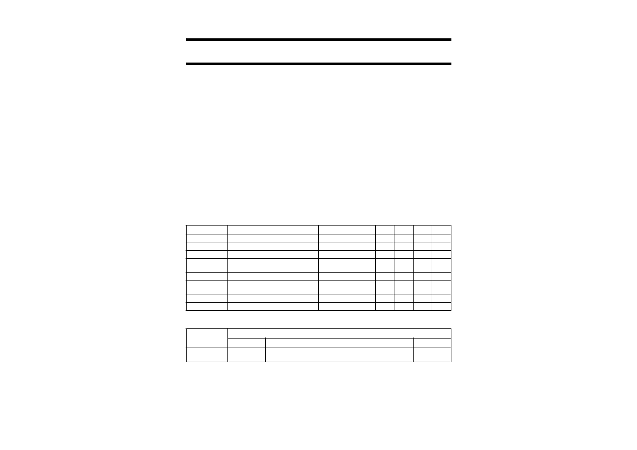
QUICK REFERENCE DATA
ORDERING INFORMATION
SYMBOL
PARAMETER
CONDITIONS
MIN.
TYP.
MAX.
UNIT
V
DD1
, V
DD2
digital supply voltage
V
DD1
= V
DD2
= V
DD
2.7
-
5.5
V
V
CC
analog supply voltage for charge pump V
CC
V
DD
2.7
-
5.5
V
I
tot
total supply current (I
DD
+ I
CC
)
V
CC
= V
DD
= 5.5 V
-
10
-
mA
I
tot(pd)
total supply current in Power-down
mode (I
DD
+ I
CC
)
logic levels 0 V or V
DD
-
5
-
µ
A
f
RF
RF input frequency
300
-
2200
MHz
f
xtal
crystal reference oscillator input
frequency
3
-
35
MHz
f
ph(comp)
phase comparator frequency
-
200
-
kHz
T
amb
operating ambient temperature
-
30
-
+85
∞
C
TYPE NUMBER
PACKAGE
NAME
DESCRIPTION
VERSION
UMA1021AM
SSOP16
plastic shrink small outline package; 16 leads; body width
4.4 mm
SOT369-1

1998 Nov 19
3
Philips Semiconductors
Product specification
Low-voltage frequency synthesizer for
radio telephones
UMA1021AM
BLOCK DIAGRAM
Fig.1 Block diagram.
handbook, full pagewidth
MGL406
CHARGE PUMP
PHASE COMPARATOR
MAIN DIVIDER
WITH
PRESCALER
REFERENCE
DIVIDER
SERIAL INTERFACE
BAND GAP
2
3
1
5
7
11
10
9
13
16
UMA1021AM
CP
4
6
8
LOCK
VSS3
RFI
VSS2
VDD2
PON
VSS1
ISET
XTAL
12
VDD1
15
VCC
14
GND(CP)
to charge pump
E
DATA
CLK
PINNING
SYMBOL
PIN
DESCRIPTION
LOCK
1
out-of-lock detector output
CP
2
charge pump output
V
DD2
3
digital supply voltage
V
SS3
4
ground 3 (0 V)
RFI
5
2 GHz main divider input
V
SS2
6
ground 2 (0 V)
PON
7
power-on input
V
SS1
8
ground 1 (0 V)
CLK
9
programming bus clock input
DATA
10
programming bus data input
E
11
programming bus enable input
(active LOW)
V
DD1
12
digital supply voltage
XTAL
13
crystal frequency input
GND(CP)
14
ground for charge pump
V
CC
15
analog supply voltage for charge
pump
I
SET
16
charge pump current setting with
external resistor from this pin to
ground
Fig.2 Pin configuration.
handbook, halfpage
UMA1021AM
MGL405
1
2
3
4
5
6
7
8
LOCK
CP
VDD2
VSS3
RFI
VSS2
PON
VSS1
ISET
VCC
GND(CP)
XTAL
VDD1
E
DATA
CLK
16
15
14
13
12
11
10
9

1998 Nov 19
4
Philips Semiconductors
Product specification
Low-voltage frequency synthesizer for
radio telephones
UMA1021AM
FUNCTIONAL DESCRIPTION
Main divider
The main divider is clocked at pin RFI by the RF signal
which is AC-coupled from an external VCO. The divider
operates with signal levels from 50 to 225 mV (RMS) and
at frequencies from 300 MHz to 2.2 GHz. It consists of a
fully programmable bipolar prescaler followed by a CMOS
counter. The main divider allows programmable ratios
from 512 to 131071 inclusive.
Reference divider
The reference divider is clocked by the signal at pin XTAL.
The applied input signal should be AC-coupled. The circuit
operates with levels from 50 up to 500 mV (RMS) and at
frequencies from 3 to 35 MHz. Any divide ratios from
8 to 2047 inclusive can be programmed.
Phase comparator and charge pump
The phase detector is driven by the edges of the output
signals of the main and reference dividers. The detector
produces current pulses at pin CP. The pulse duration is
equal to the difference in time of arrival of the edges from
the two dividers. If the main divider edge arrives first,
pin CP sinks current. If the reference divider edge arrives
first, pin CP sources current.
The current at pin CP can be controlled via the serial
programming bus as a multiple of the reference current set
by an external pull-down resistor connected between
pin I
SET
and ground (see Table 2). Pin CP remains active
except in the Power-down mode.
Additional circuitry is included to ensure that the gain of the
phase detector remains linear even for small phase errors.
Out-of-lock detector
The out-of-lock detector is enabled or disabled via the
serial interface by setting bit OOL (dt12) HIGH or LOW
(see Table 1). An open-drain transistor drives the output
pin LOCK. It is recommended to keep the sink current in
the LOW state below 400
µ
A by applying a pull-up resistor
from pin LOCK to the positive supply. When the out-of-lock
detector is enabled pin LOCK is HIGH if the error at the
phase detector input is less than approximately 25 ns,
otherwise pin LOCK is LOW. If the out-of-lock detector is
disabled, pin LOCK remains HIGH.
Serial programming bus
A simple 3-line unidirectional serial bus is used to program
the circuit.
The 3 lines are DATA (data bits), CLK (clock pulses) and
E (enable signal). The data sent to the device is loaded in
bursts framed by E. Programming clock edges and their
appropriate data bits are ignored until E goes active LOW.
The programmed information is loaded into the addressed
latch when E returns HIGH. During normal operation,
E should be kept HIGH. Only the last 21 bits serially
clocked into the device are retained within the
programming register. Additional leading bits are ignored,
and no check is made on the number of clock pulses.
The fully static CMOS design uses virtually no current
when the programming bus is inactive. It can always
capture new programmed data even during power-down.
When the synthesizer is switched on, the presence of a
signal at the reference divider input is required for correct
programming.
Data format
The data format is shown in Table 1. The first bit entered
is dt16, the last bit is ad0.
The leading bits (dt16 to dt0) make up the data field.
The four trailing bits (ad3 to ad0) are the address field.
The UMA1021AM uses 4 of the 16 available addresses.
These are chosen for compatibility with other Philips
Semiconductors radio telephone ICs. The trailing address
bits are decoded on the rising edge of E. This produces an
internal load pulse to store the data in the addressed latch.
To avoid erroneous divider ratios, the load pulse is not
allowed during data reads by the frequency dividers. This
condition is guaranteed by respecting a minimum E pulse
width after data transfer.
For the divider ratios, the first bits entered (PM16 and
PR10) are the Most Significant Bits (MSBs).
The test register (address 0000) does not normally need to
be programmed. However, if it is programmed all bits in the
data field should be set to logic 0.
Power-down mode
The synthesizer is switched on when both the power-on
input (PON) and the programmed bit dt6 (sPON) are
HIGH. When switched on, the dividers and phase detector
are synchronized to avoid random phase errors. When
switched off, the phase detector is synchronized to avoid
interrupting of the charge pump pulses.
The UMA1021AM has a very low current consumption in
the Power-down mode.
1998
Nov
19
5
Philips Semiconductors
Product specification
Low-voltage frequency synthesizer for
radio telephones
UMA1021AM
This text is here in white to force landscape pages to be rotated correctly when browsing through the pdf in the Acrobat reader.This text is here in
_
white to force landscape pages to be rotated correctly when browsing through the pdf in the Acrobat reader.This text is here inThis text is here in
white to force landscape pages to be rotated correctly when browsing through the pdf in the Acrobat reader. white to force landscape pages to be ...
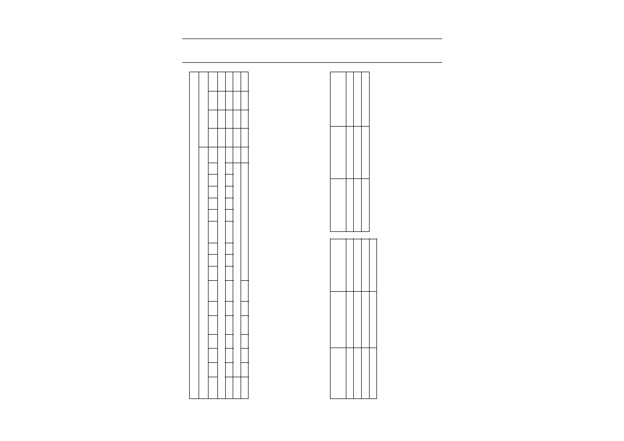
Table 1
Bit allocation; note 1
Notes
1. X = don't care.
2. The test register (address 0000) should not be programmed with any other values except all zeros for normal operation.
3. Bit OOL sets the Out-Of-Lock detector (1 = enabled).
4. Bits CR1 and CR0 set the charge pump current ratio (see Table 2).
5. Bit sPON sets the software power-up for the synthesizer (see Table 3).
6. PM16 is the MSB of the main divider coefficient.
7. PR10 is the MSB of the reference divider coefficient.
FIRST IN
REGISTER BIT ALLOCATION
LAST IN
DATA FIELD
ADDRESS
dt16
dt15 dt14 dt13
dt12
dt11
dt10
dt9
dt8 dt7
dt6
dt5 dt4 dt3 dt2 dt1
dt0
ad3
ad2
ad1
ad0
test bits; note 2
0
0
0
0
X
X
X
X
OOL
(3)
X
CR1
(4)
CR0
X
X
sPON
(5)
X
X
X
X
X
X
0
0
0
1
PM16
(6)
main divider coefficient
PM0
0
1
0
0
X
X
X
X
X
X
PR10
(7)
reference divider coefficient
PR0
0
1
0
1
Table 2
Charge pump current ratio; note 1
Note
1. Reference current for charge pump:
BIT CR1
BIT CR0
CHARGE PUMP
CURRENT
0
0
10
◊
I
set
0
1
18
◊
I
set
1
0
13
◊
I
set
1
1
17
◊
I
set
I
set
V
set
R
set
-----------
=
Table 3
Power-on programming
Notes
1. Signal level
a) L = LOW.
b) X = don't care.
c) H = HIGH.
2. X = don't care.
PIN PON
(1)
BIT sPON
(2)
SYNTHESIZER
STATE
L
X
off
X
0
off
H
1
on