VA S 9 6011/ VA S 9 6012
A d v a n c e d C o m p u t i n g
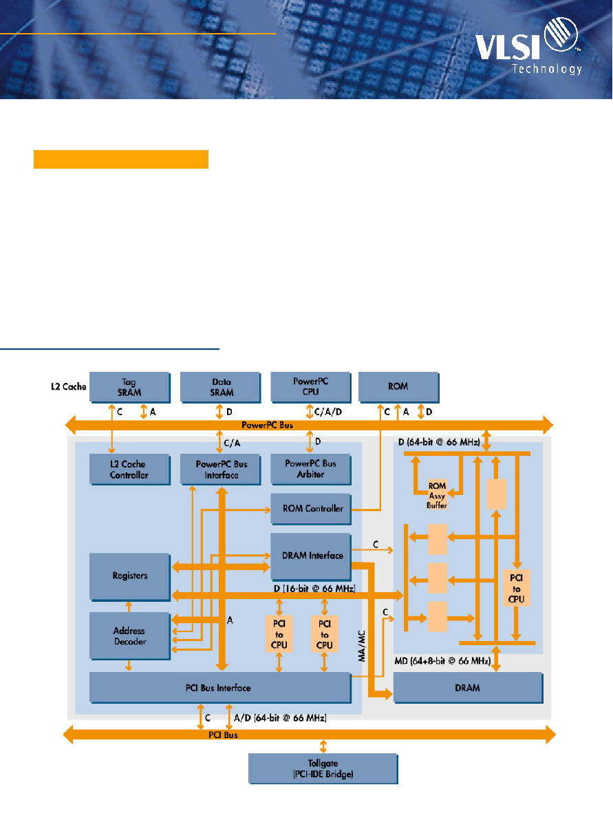
B l o c k D i a g r a m
O V E R V I E W
VLSI's VAS96011/2 is a cost-effective
core logic solution for CHRP PowerPC
platforms. The dual-chip solution
integrates system control logic and
provides a logical connection between
the PowerPC microprocessor and the
PCI bus. VAS96011/2 enable glueless
connection to the PowerPC processor,
secondary cache, system memory, ROM
and the PCI bus. This significantly
reduces overall system cost and
footprint. The VAS96011's system
memory controller supports a variety of
memory types and configurations.
The integrated secondary (L2) cache
controller supports programmable
copy back and write through modes.
Caching and shadowing of the ROM
contents are also supported to
significantly enhance ROM access
performance under MacOS.
The 32-bit PCI bus interface is opera-
tional up to 33 MHz, with program-
mable option to run synchronously
with or independent of the CPU bus
clock. All PCI bus master accesses to
main memory are snooped.
VAS96011 contains system control
logic, CPU address path and PCI inter-
face. VAS96012 is a 3-way, 64-bit wide
data path to the CPU, system memory
and VAS96011.
PowerPC System Controller

F E A T U R E S
· CHRP-compliant PowerPC system
controller
· Highly integrated dual-chip solution
· VAS96011: Address path and system
controller (240 MQFP)
· VAS96012: Data path controller
(208 MQFP)
· High performance 64-bit, 66 MHz
PowerPC CPU interface
· Supports PowerPC 603 and
604 processor families
· Integrated Phase-Locked Loop
· Secondary look-aside cache
controller
· Configurable for copy-back or
write-through operation with
direct-mapped organization
· Cache sizes of 256 KB, 512 KB, 1 MB
· Supports synchronous pipelined
burst SRAM
· Supports COASt 3.0 cache module
· Integrated tag comparator
· Caches ROM for improved ROM
access performance
· Integrated DRAM controller
· Supports Synchronous DRAM
(SDRAM), FPM-, EDO-, and
BEDO-DRAM
· 64-bit memory organization
· Addressable up to six 64-bit banks
· Glue-less connection of up to three
64-bit banks
· Supports 1 MB x 4, 16 MB x 1,
4 MB x 4, 2 MB x 8, 16 MB x 4,
and 8 MB x 8 DRAMs
· Supports symmetrical and
asymmetrical DRAM addressing
· Programmable access timing
· Integrated ROM interface controller
· S u p p o rts 2 independent ROM banks
· Supports burst cache line-fill
transactions from ROM and
flash ROM writes
· Option to boot from
PCI-based ROM
· ROM shadowing in system memory
· Integrated PCI interface controller
· Compliant with
PCI 2.1 specification
· Concurrent operation of
PowerPC and PCI buses
· Up to 33 MHz PCI bus operation
with optional synchronization to
the PowerPC bus
· Prefetching (32 bytes) of PCI reads
from system memory and of PowerPC
reads from PCI slaves
· Write FIFOs for writes from a PCI
master to system memory (64 bytes)
· Supports big- and little-endian
PCI modes
· Configuration support (IDSEL) for
up to 15 external PCI devices
· 3.3 V with 5 V-tolerant PCI pads
· 3.3V, 0.5µm technology
VLSI Technology, Inc.
1109 McKay Drive
San Jose, CA 95131
With respect to the information in this document,
VLSI Te c h n o l o g y, Inc. (VLSI) makes no guarantee or
w a rranty of its accuracy or that the use of such infor-
mation will not infringe upon the intellectual rights of
t h i rd parties. VLSI shall not be responsible for any
loss or damage of whatever nature resulting from the
use of, or reliance upon it and no patent or other
license is implied here b y. This document does not in
any way extend or modify VLSI's warranty on any
p roduct beyond that set forth in its standard term s
and conditions of sale. VLSI re s e rves the right to
make changes in its products and specifications at
any time and without notice.
LIFE SUPPORT APPLICATIONS:
V L S I 's products are not intended for use as critical
components in life suppor t appliances, devices, or
systems, in which the failure of a VLSI product to
p e rf o rm could be expected to result in personal injury.
For update information, please visit our Web site:
h t t p : / / w w w. v l s i . c o m
All brands, product names, and company names are trademarks or registered trademarks of their respective owners.
© 1997 VLSI Technology, Inc. Printed in USA
Document Control: PB-VAS96011/VAS96012
November 97