GENERAL PURPOSE PIN PHOTODIODES
SPECIFICATIONS
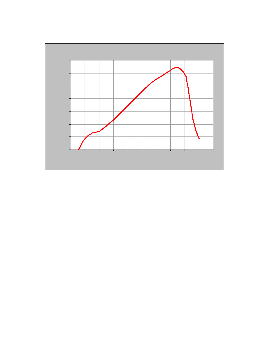
Responsivity:
0.32 A/W min., 0.38 A/W typ. @ 632.8nm; 0.50 A/W min., 0.62 A/W typ. @ 900nm
Part Number
Total
Area
Active
Area
Shunt
Resistance
1
Dark Current
1
at 5V
Breakdown
Voltage
2
at 10�A
Capacitance
3
Typ.
NEP
4
Max
Linear
Current
5
Response
Time
6
at 10V
Min.
Typ.
Max.
Typ.
at 0V
at 10V
Typ.
Typ.
Typ.
(mm
2
) (in) (M
)
(nA) (nA) (V) (pF) (pF) (W/
Hz)
(mA) (ns)
SD 057-11-21-015
1.67
0.051
x
0.051
800 0.5 2.0 50 28 6
2.8x10
-14
0.17
7
SD 057-11-21-011
1.67
0.051
x
0.051
800
0.5
2.0
50
28
6
2.8x10
-14
0.17
7
SD 076-11-21-011
isolated -211
2.91
0.105
x
0.043
450 0.9 3.5 50 50 10
3.2x10
-14
0.29 8
SD 100-11-21-021
isolated -221
5.1
0.100
(dia.)
300
1.6
6.4
50
87
18
4.0x10
-14
0.51
10
SD 125-11-21-021
7.95
0.111
x
0.111
180 2.5
10.0 50 135 28
5.2x10
-14
0.80 15
SD 172-11-21-021
isolated -221
15.4
0.185
x
0.125
100
5.0
20.0
50
255
53
7.0x10
-14
1.5
30
SD 200-11-21-041
isolated -241
20.3
0.200
(dia).
70 6.5
26.0 50 345
71
8.6x10
-14
2.03 32
SD 290-11-21-041
isolated -241
42.6
0.300
x
0.220
35
13.0
52.0
50
725
150
1.2x10
-13
4.26
70
SD 445-11-21-305
100
0.394
x
0.394
15 30.0
120 50 1700
350
2.0x10
-13
10.0 140
* All values at 23�C
1. Dark Current and Shunt Resistance vary with temperature as follows; for T23
�C, I
DT
= I
D23
* 1.09
T
,
R
SHT
= R
SH23
* 0.9
T
, where
T=(T-23) and I
D23
and R
SH23
are values at 23
�C.
2. Typical values listed. Minimum value shall be 50% of typical.
3. Typical values listed. Maximum value shall be 20% higher than the typical.
4. Test conditions are V
B
= -5V, and 950 nm.
5. In photovoltaic mode. Maximum linear current specifies the level at which the output current characteristic deviates more than 10% from the
straight line. The short circuit current saturates at approximately 10 times this level.
6. Response Time (transition time between 10% and 90% of the output signal amplitude) measured at 670 nm with a 50
load. Shorter wavelengths
will result in faster rise and fall times.
7. Storage and Operating Temperature Range for all photodiodes is -40
�C to 110�C, except for the SD
057-11-21-015 and SD
445-11-21-305, which
is �20
�C to 75�C.