PJ1085
3 Amp Low Dropout Positive Voltage Regulator
1-7
2002.rev.A
Parameter Symbol
Maximum
Units
Input Voltage
V
IN
7 V
Power Dissipation
P
D
Internally
Limited W
Thermal Resistance Junction to Case
JC
2.5
Thermal Resistance Junction to Ambient
JA
50
/W
Operating Junction Temperature Range
T
J
0 to +125
Operating Ambient Temperature Range
T
A
-20 to +85
Storage Temperature Range
T
STG
-25 to 150
Lead Temperature (Soldering) 10 Sec.
T
LEAD
260
He PJ1085 Series of high performance positive voltage
Regulators are designed for use in applications
requiring
low dropout performance at full rated current, Additionally,
the PJ1085 Series provides excellent regulation over
variations due to changes in line, load and temperature.
Outstanding features include low dropout performance at
rated current, fast transient response, internal current
limiting and thermal shutdown protection of the output
device. The PJ1085 Series are three terminal regulators with
fixed and adjustable voltage options available in popular
packages.
Low dropout voltage 1.3V max.
Full current rating over line and temperature
� Fast transient response
� Total output regulation �2% over line, load and
temperature
� Adjust pin current max 120A over temperature
� Line regulation typical 0.015%.
� Load regulation typical 0.05%.
� Fixed/adjustable output voltage
� TO-220 & TO-263 & To-252 package
Device Operating
Temperature
(Ambient)
Package
PJ1085CZ
PJ1085CZ-2.5
PJ1085CZ-3.3
TO-220
PJ1085CM
PJ1085CM-2.5
PJ1085CM-3.3
TO-263
PJ1085CP
PJ1085CP-2.5
PJ1085CP-3.3
-20 to +85
TO-252
NOTE: Contact factory for additional voltage option.
BLOCK DIAGRAM
T
TO-220 TO-263 TO-252
FEATURES
ORDERING INFORMATION
Pin: 1..Adj (Com)
2. Out
3. In
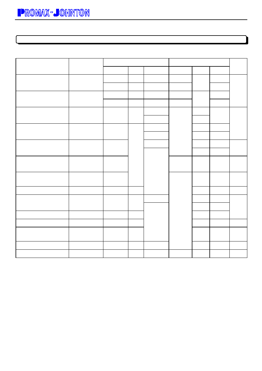
ABSOLUTE MAXIMUM RATING
PJ1085
3 Amp Low Dropout Positive Voltage Regulator
2-7
2002.rev.A
Unless otherwise specified, Adjust V
IN
= 2.75V to 12V and Adjust Io = 10mA to 3.0A
Fixed V
IN
= 4.75V to 12V and Fixed Io = 10mA to 3.0A
Test Conditions
Test Limits
Parameter
Symbol
V
IN
-V
OUT
I
O
T
J
(4)
Min
Typ
Max
Units
5V 10mA
25 0.99|Vo| 1.01|Vo|
Output Voltage
(1)
Fixed Voltage
Vo
Over
Temp.
0.98|Vo|
Vo
1.02|Vo|
5V 10mA
25 1.238
1.262
Reference Voltage
(1)
Adj Voltage
V
REF
Over
Temp.
1.225
1.250
1.275
V
25 0.015
Line Regulation
(1)
(Vin-Vout=3V)
REG
(LINE)
10mA
Over Temp.
0.035
0.2
25 0.05
0.3
Load Regulation
(1)
(Vin-Vout=3V)
REG
(LOAD)
Over Temp.
0.2
0.4
%
25 1
Dropout Voltage
V
REF
=1%
V
D
1.1 1.3
V
Current Limit
(Vin-Vout=5V)
Ic
L
3.2
4.0
A
Quiescent Current
Fixed Model
I
Q
5V
12 14 mA
Temperature Coefficient
Tc
Over Temp.
0.005 %/
25 55
Adjust Pin Current
I
ADJ
120
Adjust Pin Current Change
I
ADJ
0.2
5
A
Temperature Stability
Ts
5V
500mA
0.5
%
Minimum Load Current
Adjust Model
Io 5V
Over Temp.
5 10 mA
RMS Output Noise
(2)
V
N
25
0.003 %Vo
Ripple Rejection Ratio
(3)
R
A
5V
3.0A
Over
Temp.
60
72
dB
(1)Low duty cycle pulse testing with Kelvin connections required.
(2)Bandwidth of 10Hz to 10KHz.
(3)120Hz input ripple (C
ADJ
for ADJ)
=25F .
(4)Over Temp.-over specified operating junction temperature range.
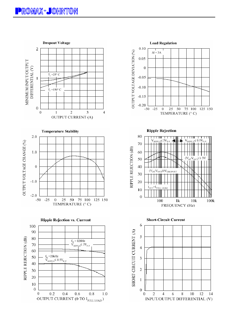
ELECTRICAL CHARACTERISTICS
PJ1085
3 Amp Low Dropout Positive Voltage Regulator
3-7
2002.rev.A
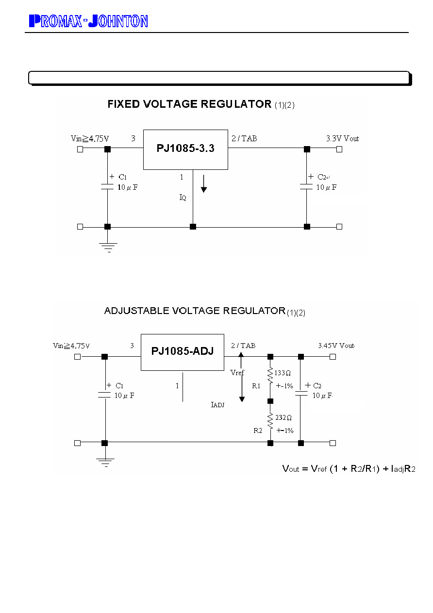
(1) C1 NEEDED IF DEVICE IS FAR FROM FILTER CAPACITORS
(2) C2 REQUIRED FOR STABILITY
(1) C1 NEEDED IF DEVICE IS FAR FROM FILTER CAPACITORS
(2) C2 REQUIRED FOR STABILITY
Typical Application Circuit