 | –≠–ª–µ–∫—Ç—Ä–æ–Ω–Ω—ã–π –∫–æ–º–ø–æ–Ω–µ–Ω—Ç: PJ2109CD | –°–∫–∞—á–∞—Ç—å:  PDF PDF  ZIP ZIP |
PJ2109
Quad Low Power Operational Amplifiers
1-4
2003/04.rev.A
Preliminary
he PJ2109 is include four independent op-amp and fixed
Voltage Reference. This device is offering space and
cost saving in many applications like power supply
management or data acquisition systems.
The PJ2109 can operate at supply Voltages as low as 3.0V or
as high as 32V with very low quiescent currents and eliminat
the necessity for external biasing components in many
applications. The output voltage range also includes the
negative power supply voltage.
∑ Low input offset voltage 2mV.
∑ Low supply current:800uA/op (@Vcc=5V)
∑ Medium Bandwidth (unity gain):0.9MHz
∑ Large output voltage range includes Ground
∑ Wide power supply range:3 to 32V
∑ Fixed output voltage reference 2.5V
∑ Voltage precision:1%
∑ Sink current capability:1 to 200mA
∑ Typical output impedance:0.2
T
Device
Operating Temperature
Package
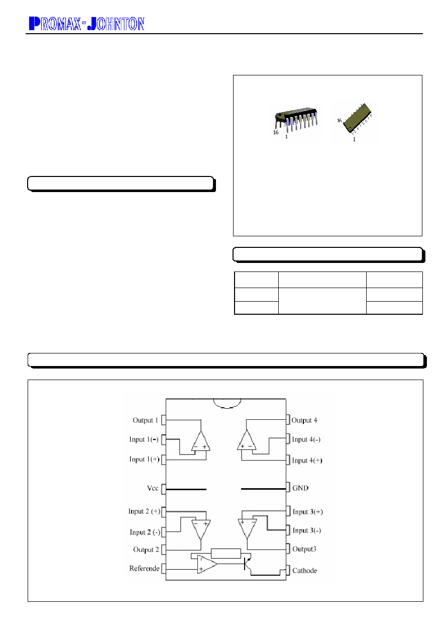
PJ2109CD
DIP16
PJ2109CS
SOP16
FEATURES
ORDERING INFORMATION
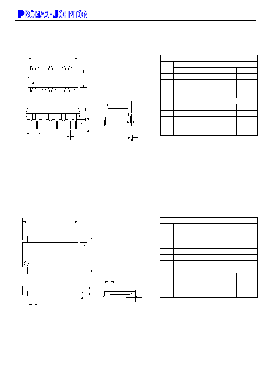
Pin:1.Output 1 9.Cathode
2.Input 1(-)
10.Input 3
3.Input 1(+)
11. Input 3(-)
4.Vcc
12 Input 3(+)
5.Input 2(+)
13. GND
6.Input 2(-)
14. Input4(+)
7.Output 2
15. Input4 (-)
8.Referenoe
16. Output 4
DIP-16
SOP-16
BLOCK DIAGRAM
-20 ~ +85

PJ2109
Quad Low Power Operational Amplifiers
2-4
2003/04.rev.A
Preliminary
PJ2109
Characteristics Symbol
Min
Typ
Max
Unit
Operaion Amplifier
Input Offset Voltage
V
CC
=5.0V to 30V
V
ICR
=0 V to V
CC
-0.7V, Vo=1.4V, Rs=0
T
A
=25
T
A
=T
high
to T
low
(Note 1)
V
IO
-
-
2.0
-
7.0
9.0
mV
Average Temperature Coefficient of Input Offset Voltage
T
A
=T
hige
to T
low
(Note 1)
I
IO
/T
-
7.0
-
V/
Input Offset Current
T
A
=T
hige
to T
low
(Note 1)
I
IO
-
-
5.0
-
50
150
nA
Average Temperature Coefficient of Input Offset Voltage
T
A
=T
hige
to T
low
(Note 1)
I
IO
/T
-
10
-
pA/
Input Bias Current
T
A
=T
hige
to T
low
(Note 1)
I
IB
-
-
-90
-
-250
-500
nA
Input Common Mode Voltage Range (Note 2)
V
CC
=30V
V
CC
=30V, T
A
=T
hige
to T
low
V
ICR
0
0
-
-
28.3
28
V
Differential Input Voltage Range
V
IDR
- - V
CC
V
Large Signal Open-Loop Voltage Gain
R
L
=2.0K, V
CC
=15V, for Large Vo Swing
T
A
=T
hige
to T
low
(Note 1)
A
VOL
25
15
100
-
-
-
V/mV
Channel Separation
10KHzf20KHz, Input Referenced
CS
- -120 - dB
Common Mode Rejection
Rs10K
CMR 65 70 - dB
Power Supply Rejection
PSR
65
100
-
dB
Output Voltage - High Limit ( T
A
=T
hige
to T
low
)
(Note 1)
V
CC
=5.0V, R
L
=10K,T
A
=25
V
CC
=30V, R
L
=2.0K
V
CC
=30V, R
L
=10K
V
OH
3.3
26
27
3.5
-
28
-
-
-
V
Output Voltage-Low Limit
V
CC
=5.0V, R
L
=10K, T
A
=T
hige
to T
low
(Note 1)
V
OL
-
5.0
20
mV
Output Source Current (V
ID
=+1.0V, V
CC
=15V)
T
A
=25
T
A
=T
hige
to T
low
(Note 1)
I
O
+
20
10
40
20
-
-
mA
Output Sink Current
(V
ID
= -1.0V, V
CC
=15V)
T
A
=25
T
A
=T
hige
to T
low
(Note 1)
(V
ID
= -1.0V, V
CC
=200mV, T
A
=25)
Io
-
10
5.0
12
20
8.0
50
-
-
-
mA
A
Output Short Circuit Ground (Note 2)
Isc
-
40 60
mA
Power Supply Current (T
A
=T
hige
to T
low
)
(Note 1)
V
CC
=30V (26V for LM2902), Vo=0V, R
L
=
V
CC
=5.0V, Vo=0V, R
L
=
Icc
-
-
-
-
3.0
1.2
mA
ELECTRICAL CHARACTERISTICS (V
CC
= 5.0V, V
EE
=GND, T
A
= 25
unless otherwise noted.)
PJ2109
Quad Low Power Operational Amplifiers
3-4
2003/04.rev.A
Preliminary
PJ2109
Characteristic Symbol
Min
Typ
Max
Unit
Operaion Amplifier
Reference Input Voltage (Figure 1)
V
KA
= V
ref
, I
K
= 10 mA, T
A
= +25
T
A
= T
low
to T
high
(Note 1)
PJ2109
Vref
2.475 2.495 2.525
Reference Input Voltage Deviation Over
Temperature Range (Figure 1, Note 1,2,4)
V
KA
= V
ref
, I
K
= 10 mA
Vref
-- 3.0 17 mV
Minimum Cathode Current for Regulation
V
KA
= V
ref
(Figure 1)
I
min
-- 0.15 0.3 mA
Off-State Cathode Current (Figure 3)
V
KA
= 36 V, V
ref
= 0V
I
off
-- 2.6 1000 nA
Dynamic Impedance (Figure 1, Note 3)
V
KA
= V
ref
,
I
K
= 1.0 mA to 100 mA, f
1.0 kHz
| Z
ke
|
-- 0.22 0.5
Note: 1. Short circuits from the output to Vcc can cause excessive heating and eventual destruction . Destructive dissipation can
result from simultaneous shorts on all amplifiers.
2. The input common mode voltage or either input signal voltage should not be allowed to go negative by more than 0.3V
The upper end of the common mode voltage range is Vcc-1.7V.
VOLTAGE REFERENCE
PJ2109
Quad Low Power Operational Amplifiers
4-4
2003/04.rev.A
Preliminary
DIP-16 Unitmm
G
K
D
C
N
A
1
16
B
8
9
M
J
L
DIP-16 DIMENSION
MILLIMETERS INCHES
DIM
MIN MAX MIN MAX
A 1.780 18.050 0.701 0.710
B 6.250 6.450 0.292 0.299
C 2.350 2.650 0.093 0.104
D 0.350 0.490 0.014 0.019
G 1.27BSC
0.05BSC
J 0.250 0.320 0.010 0.012
K 0.100 0.250 0.004 0.009
L 7.750 8.000 0.305 0.315
M 0∞ 10∞
0∞ 10∞
N 0.390 1.010 0.015 0.039
SOP-16 Unitmm
A
1
D
16
P
B
C
K
8
9
R
F
SOP-16 DIMENSION
MILLIMETERS INCHES
DIM
MIN MAX MIN MAX
A 9.800 10.000 0.368 0.393
B 7.400 7.600 0.292 0.299
C 2.350 2.650 0.093 0.104
D 0.350 0.490 0.014 0.019
F 0.500 0.900 0.020 0.035
G 1.27BSC
0.05BSC
K 0.100 0.250 0.004 0.009
M 0 7 0
7
P 10.05 10.55 0.395 0.415
R 0.250 0.75 0.010 0.029