PJ2700 Series
Low Noise CMOS Positive Voltage Regulators
1-5
2002/10.rev.A
he PJ2700 series are highly precise, low noise, ultra low
power consumption, positive voltage regulators
manufactured using CMOS and laser trimming technologies.
The series provides large currents with a significantly small
dropout voltage. The PJ2700 consists of a current limiter
circuit, a driver transistor, a precision reference voltage and an
error amplifier. Output voltage is selectable in 0.1V steps
between 2.0V ~ 6.0V in TO-92, SOT-89 and SOT-23 packages are
available.
Maximum Output Current:300mA
Dropout Voltage :300mV @ 100mA
Maximum Operating Voltage : 10V
Output Voltage Range :2.0V~6.0V(selectable in 0.1V steps)
Highly Accurate : ±2%
Low Power Consumption : TYP 2µA at Vout=5.0V
Operational Temperature Range : -20 ~ 85
Ultra Small Packages : TO-92, SOT-89, SOT-23
Applications
Mobile phones
Cordless phones
Cameras, video recorders
Portable games
Portable AV equipment
CD-Rom, DVD and LAN Card
Battery powered equipment
Device Operation
Temperature
Package
PJ27xxCT TO-92
PJ27xxCY SOT-89
PJ27xxCX
-20 ~ +85
o
C
SOT-23
Remark: xx is output voltage, ex 33 = 3.3V, 25 = 2.5V
T
FEATURES
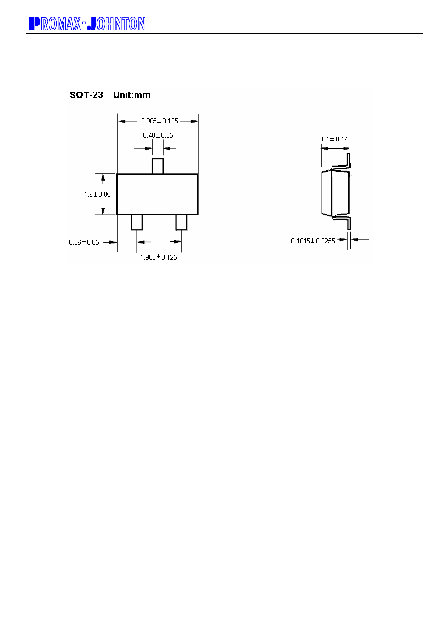
SOT-89
SOT-23
ORDER INFORMATION
BLOCK DIAGRAM
Pin 1. Gnd
2. In
3. Out
(Heatsink surface connected to Pin 2)
Pin 1. Gnd
2. Out
3. In
TO-92
Pin 1.Gnd
2. In
3. Out

PJ2700 Series
Low Noise CMOS Positive Voltage Regulators
2-5
2002/10.rev.A
Parameter
Symbol Value
Unit
Input Voltage
V
IN
10 V
Output Current
I
OUT
300 mA
Output Voltage
V
OUT
Vss-0.3
~
V
IN
+0.3
V
Power Dissipation TO-92
SOT-89
SOT-23
Pd
625
550
300
mW
Operating Temp
Topr
-20 ~ +85
Storage Temp
Tstg
-40 ~ +125
Parameter Symbol
Conditions
Min Typ Max Unit
Circuit
Output Voltage
V
OUT
(E)
(Note 2)
I
OUT
=40mA
V
IN
=V
OUT
+ 1V
-2% -- +2% V 2
Maximum Output Current
I
OUT
max
V
IN
= V
OUT
+
1V,
300 -- -- mA 2
Load Regulation
V
OUT
V
IN
= V
OUT
+ 1V
1mA
I
OUT
100mA
-- 45 90 mV --
Dropout Voltage (Note3)
Vdif 1
Vdif 2
Vdif 3
I
OUT
=80mA
I
OUT
=160mA
Iout=300mA
--
200
450
800
360
700
950
mV 2
Supply Current
Iss
V
IN
= V
OUT
+ 1V
--
3.0
5.0
µA
1
Line Regulation
V
OUT
V
IN
∑
V
OUT
I
OUT
=40mA
V
OUT
+ 1VVin
10V
-- 0.2 0.3
%/V 2
Input Voltage
V
IN
--
--
--
10
V
--
Output Voltage
Temperature Characteristics
V
OUT
Topr
∑
V
OUT
I
OUT
=40mA
-40
o
CTopr
85
o
C
-- ±100 -- ppm/
o
C
2
Note: 1. V
OUT
(T)=
Specified Output Voltage.
2. V
OUT
(E)
=Effective output Voltage (i.e. the output voltage when "V
OUT
(T)+1.0" is provided while maintaining a certain
I
OUT
value).
3. Vdif={V
IN
1(Note5)- V
OUT
1(Note4)}
4.
V
OUT
1=A voltage equal to 98% of the output voltage when a stabilized (V
OUT
(T)
+1.0V) is input.
5.
V
IN
=The input voltage at the time V
OUT
1
is output (input voltage has been gradually reduced).
ABSOLUTE MAXIMUM RATINGS
ELECTRICAL CHARACTERISTICS
(Ta = +25∞C, Cin = Cout = 1uF unless otherwise noted)

PJ2700 Series
Low Noise CMOS Positive Voltage Regulators
3-5
2002/10.rev.A
Measuring Circuit 1: Supply Current
Measuring Circuit 2: Output Voltage, Oscillation Check, Line Regulation, Dropout Voltage, Load Regulation
TYPICAL APPLICATIONS
MEASURING CIRCUITS