
PJ3100Series
300mA CMOS LDO With Enable
1-9
2002/11.rev.A
he PJ3100 family is a positive voltage linear regulator
developed utilizing CMOS technology featured low
quiescent current (30µA typ), low dropout voltage, and high
output voltage accuracy, making them ideal for battery
applications. EN input connected to CMOS has low bias
current. The space-saving SOT-23-5L package is attractive for
"Pocket" and "Hand Held" application.
These rugged devices have both Thermal Shutdown, and
Current Fold-back to prevent device failure under the "Worst"
of operating conditions.
In application requiring a low noise, regulated supply, place a
1000pF capacitor between Bypass and Ground.
The PJ3100 is stable with an output capacitance of 2.2µF or
greater.
Very Low Dropout Voltage
High Accuracy Output Voltage: ±1.5%
Low Current Consumption : Typ. 30µA, Max. 35µA
Output Voltage Range :1.5V, 1.8V, 1.9V, 2.2V, 2.5V, 2.7V,
2.8V, 3.3V, 3.5V, 3.6V, and 3.8V
Thermal Shutdown
Low Temperature Coefficient
Battery-powered devices
Personal communication devices
Home electric/electronic application
PC peripherals
Short Circuit Current Fold-Back
Compact package : SOT-23-5
Factory Pre-set Output Voltage
Current Limiting
Input Range of 2.6V to 7.0V
Guaranteed 300mA Output
T
FEATURES
SOT-23-5
ORDER INFORMATION
TYPICAL APPLICATIONS
Pin:
1. Vin 4. BYP
2. Gnd 5. Vout
3. EN
Device
Operation Temperature
(Ambient)
Package
PJ3100CX -40 ~ +85
o
C SOT-23-5
APPLICATION
PJ3100Series
300mA CMOS LDO With Enable
2-9
2002/11.rev.A
Parameter
Symbol Value
Unit
Input Voltage
V
IN
7 V
Output Current
I
OUT
P
D
/ (V
IN
≠ Vo)
mA
Output Voltage
V
OUT
GND-0.3V
~
V
IN
+0.3
V
Junction Temperature
Tj
-40 ~ +125
Storage Temp.
Tstg
-40 ~ +125
Parameter
Maximum Unit
Thermal Resistance (
JC
) SOT-23-5
260
/W
Internal Power Dissipation (P
D
)
(T = 100)
SOT-23-5 380
/W
Maximum Junction Temperature
150
Maximum Lead Temperature
300
ABSOLUTE MAXIMUM RATINGS
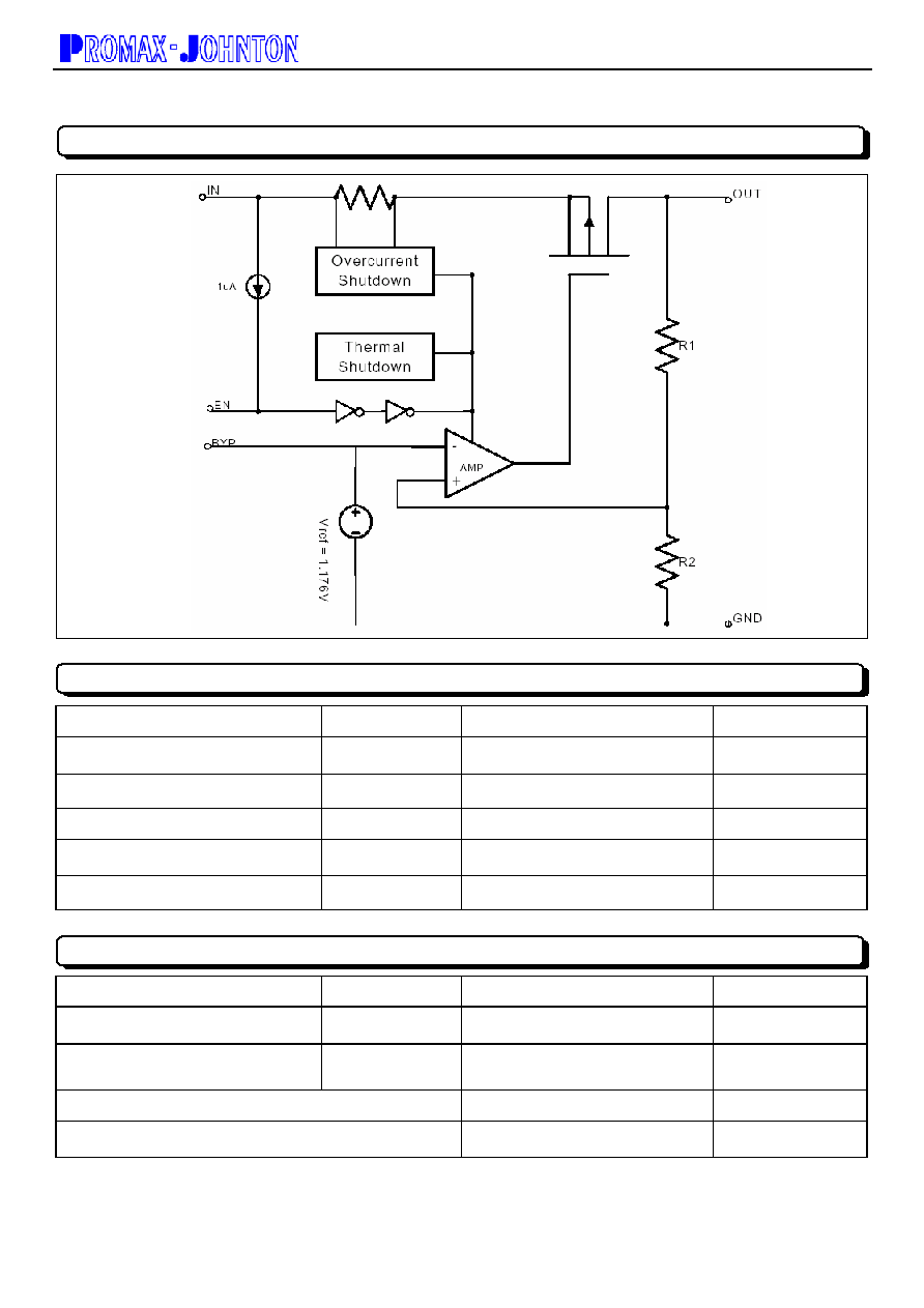
BLOCK DIAGRAM
THERMAL INFORMATION

PJ3100Series
300mA CMOS LDO With Enable
3-9
2002/11.rev.A
Parameter Symbol Test
Conditions Min
Typ
Max
Unit
Input Voltage
V
IN
Note
1
7
V
Output Voltage Accuracy
V
OUT
I
O
=1mA ~ 300mA
-2
2
%
Load Regulation
REG
LOAD
Io=1mA ~ 300mA
0.2
1
%
V
OUT
<=3.0V
-0.15 0.03 0.15 %
Line Regulation
REG
LINE
I
o
=5mA, VIN= V
OUT
+1
to V
OUT
+2
V
OUT
>3.0V
-0.3
0.06
0.3
%
Io=300mA,V
OUT
=V
O(NOM)
-2%, V
OUT
>=2.5V
300
Dropout Voltage
V
DROPOUT
Io=300mA,V
OUT
=V
O(NOM)
-2%, V
OUT
<2.5V
800
mV
Output Current
Io
V
OUT
> 1.2V
300
mA
Current Limit
I
LIMIT
V
OUT
> 1.2V
300
450
mA
Short Circuit Current
Isc
V
OUT
< 0.95V
150
300
mA
Quiescent Current
I
Q
Io = 0mA
30
35
µA
Ground Pin Current
I
GND
Io = 1mA ~ 300mA
30
50
µA
Over Temperature Shutdown
OTS
150
Over Temperature Hysteresis
OTH
30
V
OUT
Temperature Coefficient
TC
25
ppm/
f=1KHz 60
f=10KHz 50
Power Supply Rejection
PSRR
Io = 100mA
Co=2.2µF ceramic
f=100KHz 40
dB
f=1KHz 75
f=10KHz 55
Power Supply Rejection
PSRR
Io = 100mA
Co=2.2µF ceramic
C
BYP
=0.01µF
f=100KHz 30
dB
Co=2.2µF 30
Output Voltage Noise
eN
f=10Hz to 100KHz
Io=10mA, C
BYP
=0µF
Co=100µF 20
µVrms
Co=2.2µF 30
Output Voltage Noise
eN
f=10Hz to 100KHz
Io=10mA,C
BYP
=0.01µF
Co=100µF 20
µVrms
Shutdown Supply Current
I
SD
V
IN
=5V, V
OUT
=0V, V
EN
<V
EL
2.0
3.0
µA
I
EH
V
EN
=V
EL,
V
IN
=2.6V~7V
0.1
EN Input Bias Current
I
EL
V
EN
=V
EL,
V
IN
=2.6V~7V
1.0
3.0
µA
V
EH
V
IN
=2.6V~7V
V
IN
/2+0.8V
V
IN
EN Input Threshold
V
EL
V
IN
=2.6V~7V 0
V
IN
/2-0.8V
V
Note: 1. V
IN(MIN)
= V
OUT
+V
DROPOUT
ELECTRICAL CHARACTERISTICS
(Ta = +25∞C unless otherwise noted)
PJ3100Series
300mA CMOS LDO With Enable
4-9
2002/11.rev.A
DETAILED DESCRIPTION
The PJ3100 family of CMOS regulators contain a PMOS pass transistor, voltage reference, error amplifier, over-current protection,
thermal shutdown, and short circuit protection.
The P-channel pass transistor receives data from the error amplifier, over current shutdown, short output protection, and thermal
protection circuits. During normal operation, the error amplifier compares the output voltage to a precision reference. Over-current
and Thermal shutdown circuits become active when the junction temperature exceeds 150, or the current exceeds 300mA.
During thermal shutdown, the output voltage remains low. Normal operation is restored when the junction temperature drops
below 120.
The PJ3100 switches from voltage mode to current mode when the load exceeds the rated output current. This prevents over-stress.
The PJ3100 also incorporates current fold-back to reduce power dissipation when the output is short-circuited. This feature
becomes active when the output drops below 1.05V, and reduces the current flow by 65%. Full current is restored when the
voltage exceeds 0.95V.
ENABLE
The Enable pin normally floats high. When actively, pulled low, the PMOS pass transistor shut off, and all internal circuits are
powered down. In this state, the quiescent current is less than 2µA. This pin behaves much like an electronic switch.
EXTERNAL CAPACITOR
The PJ3100 is stable with an output capacitor to ground of 2.2µF or greater. It can keep stable even with higher or poor ESR
capacitors. A second capacitor is recommended between the input and ground to stabilize VIN. The input capacitor should be
larger than 0.1uF to have a beneficial effect. All capacitors should be placed in close proximity to the pins. A "quiet" ground
termination is desirable.
Part Number
Output Voltage Voltage
Code
Package
PJ3115CX 1.5V
A
SOT-23-5L
PJ3118CX 1.8V
D
SOT-23-5L
PJ3119CX 1.9V
E
SOT-23-5L
PJ3122CX 2.2V
H
SOT-23-5L
PJ3125CX 2.5V
K
SOT-23-5L
PJ3127CX 2.7V
M
SOT-23-5L
PJ3128CX 2.8V
N
SOT-23-5L
PJ3129CX 2.9V
O
SOT-23-5L
PJ3130CX 3.0V
P
SOT-23-5L
PJ3133CX 3.3V
S
SOT-23-5L
PJ3135CX 3.5V
U
SOT-23-5L
PJ3136CX 3.6V
V
SOT-23-5L
PJ3138CX 3.8V
X
SOT-23-5L
ORDERING INFORMATION
