 | –≠–ª–µ–∫—Ç—Ä–æ–Ω–Ω—ã–π –∫–æ–º–ø–æ–Ω–µ–Ω—Ç: PJ4558CS | –°–∫–∞—á–∞—Ç—å:  PDF PDF  ZIP ZIP |

PJ4558
Dual Wide Bandwidth Operational Amplifiers
1-5
2003/04.ver.B
Preliminary
2.5MHz Unity Gain Bandwidth Guaranteed(PJ4558)
Internally Compensated
Short Circuit Protection
Gain and Phase Match between Amplifiers
Low Power Consumption
Device Operating
Temperature Package
PJ4558CS SOP-8
PJ4558CD
-20~ +85
DIP-8
DIP-8
SOP-8
Pin: 1.Output A 5. Input B
2.Input A 6. Input B
3.Input A 7. Output B
4.V
EE
8.Vcc
FEATURES
MAXIMUM RATINGS
(T
A
=25, unless otherwise noted)
Rating Symbol
PJ4558
Unit
Power Supply Voltage
Vcc
V
EE
+22
-22
Vdc
Input Differential Voltage
V
ID
±
30
V
Input Common Mode Voltage
(Note 1)
V
ICM
±
15
V
Output Short Circuit Duration
(Note 2)
tsc Continuous --
Ambient Temperature Range
T
A
-20 to 85
Storage Temperature Range
Tstg
5 to 125
Junction Temperature
T
J
150
ORDERING INFORMATION
BLOCK DIAGRAM

PJ4558
Dual Wide Bandwidth Operational Amplifiers
2-5
2003/04.ver.B
Preliminary
Input Offset Voltage(Rs10K)
V
IO
-- 1.0 5.0 mV
Input Offset Current
I
IO
-- 20 200 nA
Input Bias Current(Note 1)
I
IB
-- 80 500 nA
Input Resistance
rj
0.3
2.0
--
M
Input Capacitance
Cj
--
1.4
--
pF
Common Mode Input Voltage Range
V
ICR
±
12
±
13
-- V
Large Signal Voltage Gain
(Vo=±10V,R
L
=2.0K)
A
VOL
50 200 --
V/mV
Output Resistance
ro
--
75
--
Common Mode Rejection(Rs10K)
CMR 70
90 --
dB
Supply Voltage Rejection Ratio(Rs10K)
PSRR --
30 150 V/V
Output Voltage Swing
(R
L
10K)
(R
L
2.0K)
Vo
±
12
±
10
±
14
±
13
--
--
V
Output Short Circuit Current
Isc
10
20
40
mA
Supply Currents(Both Amplifiers)
I
D
-- 2.3 5.0 mA
Power Consumption(Both Amplifiers)
Pc
--
70
150
mW
Transient Reponse(Unity Gain)
(V
I
=20mV , R
L
2.0K, C
L
100pF)Rise Time
(V
I
=20mV , R
L
2.0K, C
L
100pF)Overshoot
(V
I
=10V , R
L
2.0K, C
L
100pF)Slew Rate
t
TLH
os
SR
--
--
1.5
0.3
15
1.6
--
--
--
s
%
V/s
Input Offset Votlage(Rs10K)
V
IO
- 1.0 6.0 mV
Input Offset Current
(T
A
=Thigh)
(T
A
=Tlow)
(T
A
=0 to 70)
I
IO
--
--
--
7.0
85
--
200
500
--
nA
Input Bias Current
(T
A
=Thigh)
(T
A
=Tlow)
(T
A
=0 to 70)
I
IB
--
--
--
30
300
--
500
1500
--
nA
Common Mode Input Voltage Range
V
ICR
±
12
±
13
-- V
Large Signal Voltage Gain(Vo=±10V,R
L
=2.0 K
)
A
VOL
26
-- --
V/mV
Common Mode Rejection(Rs10K)
CMR 70
90 --
dB
Supply Voltage Rejection Ratio(Rs10K)
PSRR --
30 150 V/V
Output Voltage Swing
(R
L
10K)
(R
L
2.0K)
Vo
±
12
±
10
±
14
±
13
--
--
V
Supply currents(Both Amplifiers)
(T
A
=Thigh)
(T
A
=Tlow)
I
D
--
--
--
--
4.5
6.0
mA
Power Consumption(Both Amplifiers)
(T
A
=Thigh)
(T
A
=Tlow)
Pc
--
--
--
--
135
180
mW
Notes:1. I
IB
is
out of amplifier due to PNP input transistors. 2.T high=70, T low=0.
ELECTRICAL CHARACTERISTICS
(Vcc=+15V,V
EE
= -15V,T
A
=Thigh to Tlow,unless otherwise noted)
ELECTRICAL CHARACTERISTICS
(Vcc=+15V,V
EE
= -15V, T
A
=25,unless otherwise noted)

PJ4558
Dual Wide Bandwidth Operational Amplifiers
3-5
2003/04.ver.B
Preliminary
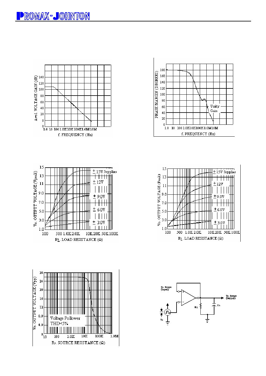
Figure 1.Burst Noise versus Source Resistance
Figure 3.Output Noise Versus Source Resistance
Unlike conventional peak reading or RMS meters, this system
was especially designed to provide the quick response time
essential to burst(popcorn) noise testing.
Figure 2.RMS Noise versus Source Resistance
Figure 4.Spectrial Noise Density
The test time employed is 10 sec and the 20Vpeak limit
refers to the operational amplifier input thus eliminating
errors in the closed loop gain factor of the operational
amplifier.
Figure 5.Burse Noise Test Circuit
PJ4558
Dual Wide Bandwidth Operational Amplifiers
4-5
2003/04.ver.B
Preliminary
Figure 6. Open Loop Frequency Response
Figure 8.Positive Output Voltage Swing versus Load
Resistance
Figure 10.Power Bandwidth (Large Signal Swing versus
Frequency)
Figure 7.Phase Margin versus Frequency
Figure 9.Negative Output Voltage Swing versus Load
Resistance
Figure 11.Transient Response Test Circuit
PJ4558
Dual Wide Bandwidth Operational Amplifiers
5-5
2003/04.ver.B
Preliminary
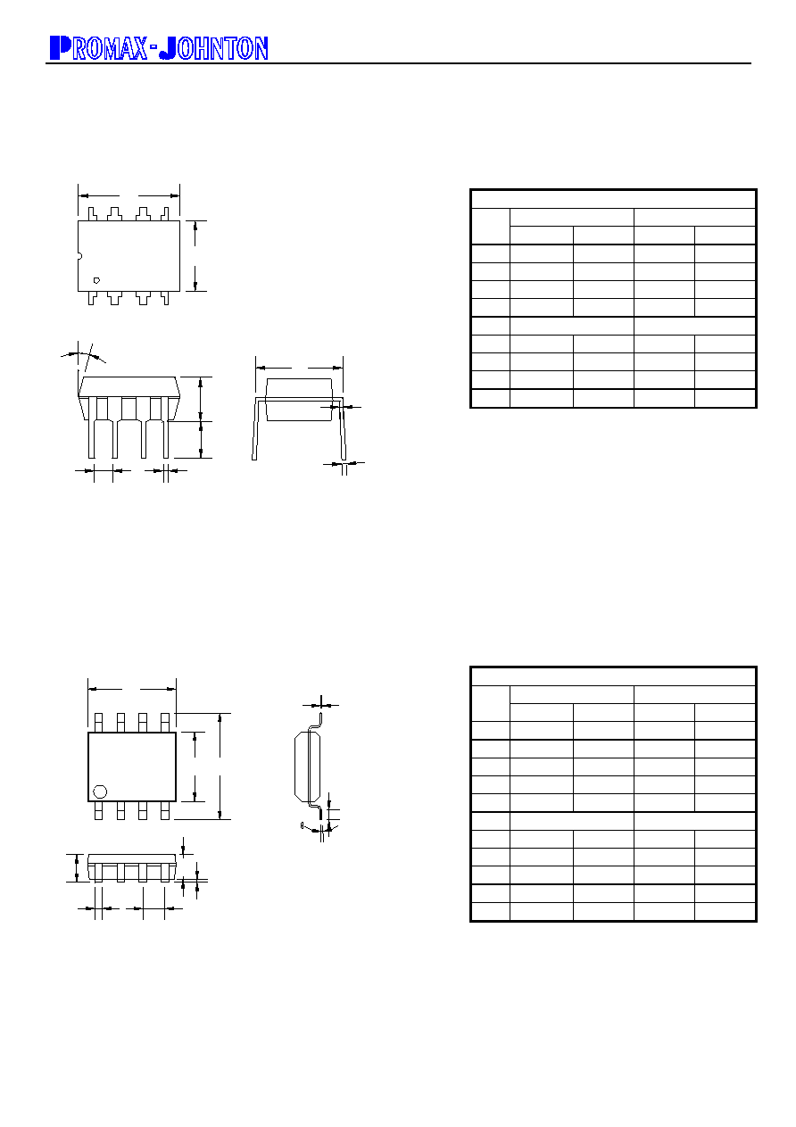
DIP-8 DIMENSION
MILLIMETERS INCHES
DIM
MIN MAX MIN MAX
A 9.070 9.320 0.357 0.367
B 6.220 6.480 0.245 0.255
C 3.180 4.430 0.125 0.174
D 0.350 0.550 0.019 0.022
G 2.54BSC
0.10BSC
J 0.150 0.290 0.006 0.011
K 3.250 3.350 0.128 0.132
L 7.750 8.000 0.305 0.315
M - 10∞ - 10∞
DIP-8 Unitmm
7∞
K
D
G
C
A
1
8
B
4
5
L
M
J
SOP-8 Unitmm
B
C
H
G
1
D
E
F
4
A
8
5
J
I
SOP-8 DIMENSION
MILLIMETERS INCHES
DIM
MIN MAX MIN MAX
A 4.800 5.000 0.189 0.197
B 3.800 4.000 0.150 0.157
C 5.800 6.200 0.228 0.244
D 1.400 1.500 0.055 0.059
E - 0.100 - 0.004
F 1.27BSC
0.05BSC
G 0.330 0.510 0.013 0.020
H 1.450 1.550 0.057 0.061
I 0.190 0.250 0.007 0.010
J 0.400 1.270 0.016 0.050
0∞
8∞
0∞
8∞