PJ4800 Series
400mA Low Dropout Voltage Regulators
1-6 2002/01.rev.A
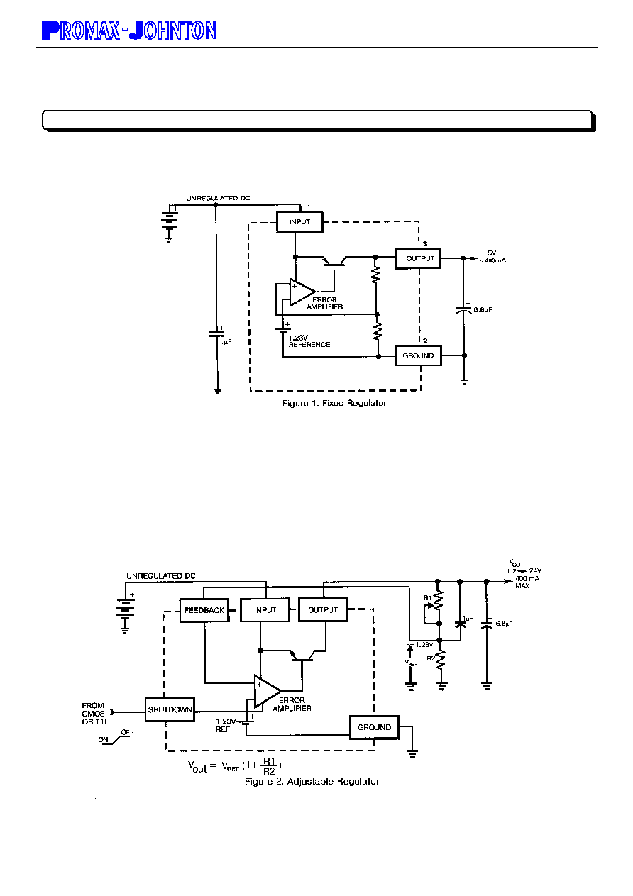
he series of fixed-voltage monolithic micropower voltage
regulators is designed for a wide range of applications.
Thes device excellent choice fo use in battery-power
application. Furthermore, the quiescent current increases on
slightly at dropout, which prolongs battery life.
This series of fixed-voltage regulators features very low
quiescent current ( 100mA Typ.) and very low drop output
voltage (Typ. 60mV al light load and 600mV at 400mA).
This includes a tight initial tolerance of 0.5% typ., extremely
good load and line regulation of 0.05% typ., and very low
output temperature coefficient.
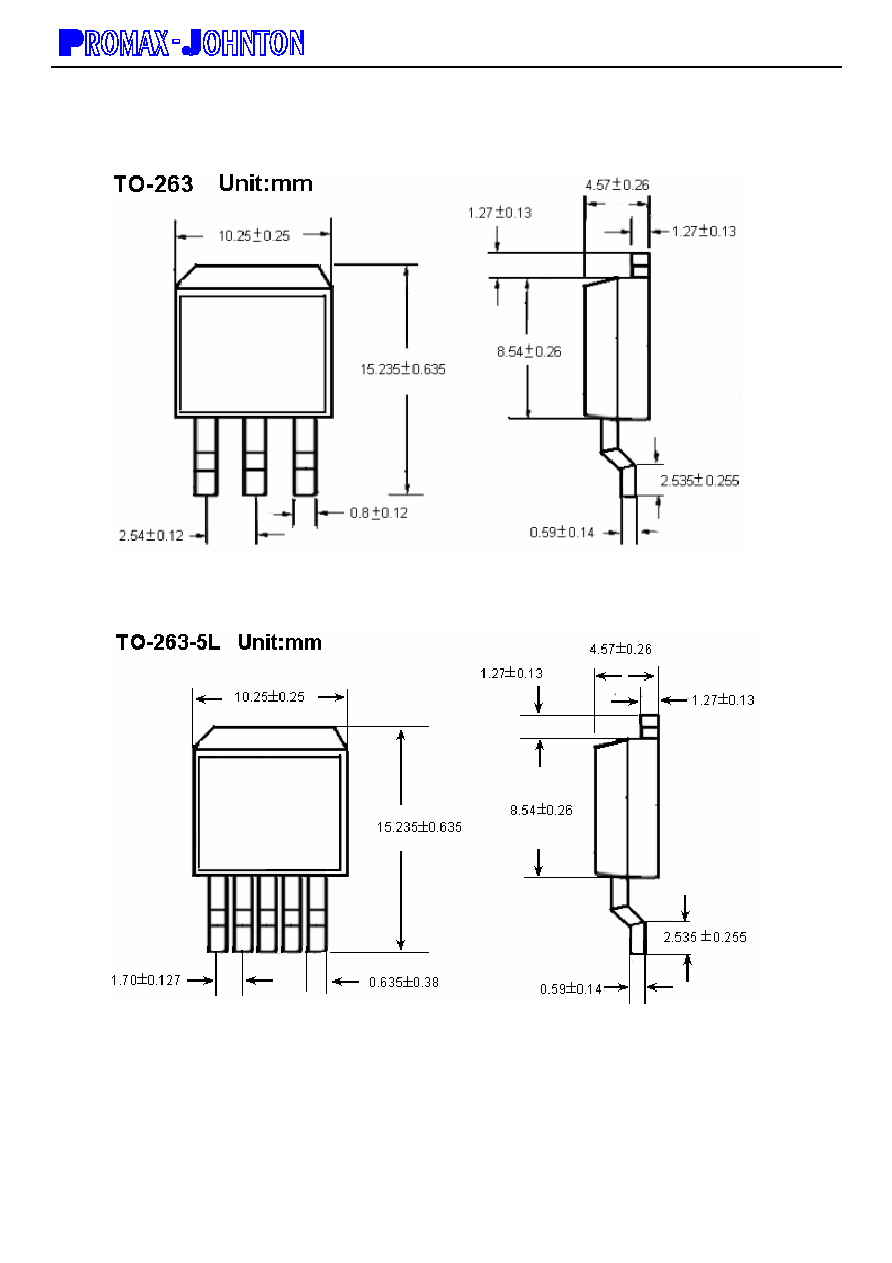
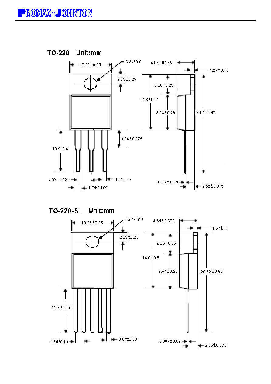
This series is offered in 3-pin TO-263, TO-220, TO-252 &
SOT-223 package, and in 5-pin TO-220 & TO-263 package
with shutdown input.
______________________________________________________________
______________________________________
∑ Output accuracy within 2% at over timperature
∑ Very low quiescent current
∑ Low dropout voltage (400mV Typ)
∑ Extremely tight load and line regulation
∑ Very low temperature coefficient
∑ Unregulated DC input can withstand -20V reverse battery
and +60V positive transients
∑ Avaiable Output Voltage 5V, 3.3V, 2.5V, 1.8V
∑
High-efficiency linear regulator
∑
Battery powered systems
∑
Portable instrumentation
∑
Portable consumer equipment
∑
Portable / Palm top / Notebook computers
∑
Automotive electronics
∑ SMPS Post-Regulator
Device Operating
Temperature
Package
PJ48xxCZ-5L TO-220-5L
PJ48xxCM-5L
TO-263-5L
PJ48xxCZ TO-220
PJ48xxCM TO-263
PJ48xxCP TO-252
PJ48xxCW
-20 to +85
SOT-223
xx- output voltage
Power Dissipation
Internally Limited
Lead Temperature (Soldering, 5 seconds)
260
Storage Temperature Range
.-65 to +150
Operating Junction Temperature Range
-55 to +150
Input Supply Voltage
-20 to +35V
Continuous total dissipation at 25 free-air temperature TO-220/TO-263
TO-252
SOT-223
2W
1W
0.8W
T
FEATURES
APPLICATIONS
ORDERING INFORMATION
TO-220-5L
TO-263-5L
SOT-223 / TO-252
TO-220 / TO-263
PIN 1. Error
2. Input
3. Ground
4. Output
5. Shutdown
ABSOLUTE MAXIMUM RATINGS
PIN 1. Input
2. Ground
3. Output
PJ4800 Series
400mA Low Dropout Voltage Regulators
2-6 2002/01.rev.A
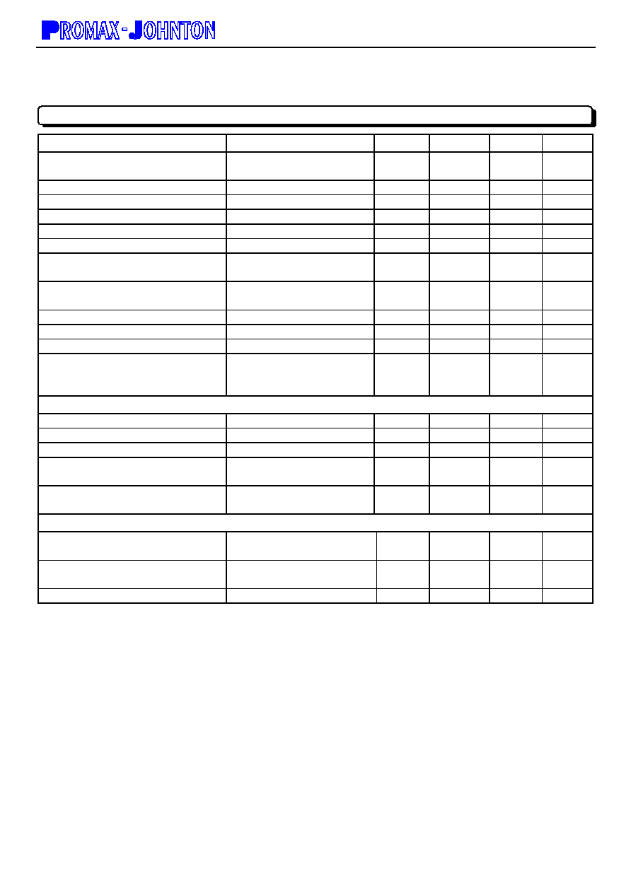
Parameter Conditions
Min
Typ
Max
UNITS
Output Voltage
T
J
=25
Full Operating Temperature
0.980|Vo|
0.970|Vo||
5.0 / 3.3
2.5 / 1.8
1.020|Vo|
1.030|Vo|
V
Output Voltage
1mA
I
L
700mA, T
J
T
JMAX
0.965|Vo|
1.035|Vo|
V
Input Supply Voltage
26
V
Output VoltageTemperature Coefficient
(Note 1)
50
150
ppm/
Line Regulation (Note 2)
13V
V
in
26V (Note 3)
0.1
0.4
%
Load Regulation (Note 2)
1mA
I
L
700mA
0.1
0.3
%
Dropout Voltage (Note 4)
I
L
=100mA
I
L
=400mA
200
400
300
600
mV
mV
Ground Current (Note 5)
I
L
=100
A
I
L
=400mA
100
30
200
40
A
mA
Dropout Ground Current (Note 5)
V
in
=Vout-0.5V, I
L
=100A
200
300
A
Current Limit
V
out
=0
700
900
mA
Thermal Regulation (Note 6)
0.05
0.2
%W
Output Noise,
10Hz
to 100KHz,
I
L
=400mA
C
L
=2.2F
C
L
=3.3F
C
L
=33F
500
350
120
Vrms
Adjust Model
Reference Voltage
1.21 1.235 1.26 V
Reference Voltage
Over Temperature (Note 7)
1.185 1.285
V
Feedback Pin Bias Current
20
40
nA
Reference Voltage Temperature
Coefficient
(Note 1)
50
ppm/
Feedback Pin Bias Current Temperature
Coefficient
0.1
nA/
Shutdown Input
Input Logic Voltage
Low (Regulator ON)
High (Regulator OFF)
2
0.7 V
Shutdown Pin Input Current
Vs = 2.4V
Vs = 26V
30
450
50
600
A
Regulator Output Current in Shutdown (Note 8)
200
A
Note 1: Output or reference voltage temperature coefficients defined as the worst case voltage change divided by the tatal
temperature range.
Note 2: Regulations is measured at constant junction temperature, using pulse testing with a low duty cycle. Changes in output
voltage due to heating effects are covered under the specification for thermal regulation.
Note 3: Line regulation is tested at 125 for I
L
= 5mA. For I
L
= 100A and T
J
= 125, line regulation is guaranteed by desigh to
0.2%. for 13V
V
in
26V.
Note 4: Dropout voltage is defined as the input to output differential at which the output voltage drops2% below its nominal value
measured at 1V differential.
Note 5: Ground pin current is the regulator quiescent current. The total current drawn from the source is the sum of the ground pin
current and output load current.
Note 6: Thermal regulation is the change in output voltage at a time T after a change in power dissipation, excluding load or line
regulation effects. Specifications are for a 200mA load pulse(3W pulse) for T = 10ms.
Note 7: Vref
Vou t (Vin-1V), 2.3V Vin 26V, 100A I
L
400mA,
T
J
T
JMAX
.
Note 8: 2V
Vshutdown, Vin 26V, Vout = 0V
ELECTRICAL CHARACTERISTICS at
Vin = 14.4V, Ta = 25, I
L
= 5mA, C
o
= 100F, unless otherwise noted.