 | –≠–ª–µ–∫—Ç—Ä–æ–Ω–Ω—ã–π –∫–æ–º–ø–æ–Ω–µ–Ω—Ç: P102-05SC | –°–∫–∞—á–∞—Ç—å:  PDF PDF  ZIP ZIP |
PLL102-05
Low Skew Output Buffer
47745 Fremont Blvd., Fremont, California 94538 Tel (510) 492-0990 Fax (510) 492-0991 www.phaselink.com Rev 09/22/05 Page 1
FEATURES
∑ Frequency range 25 ~ 60MHz.
∑ Internal phase locked loop will allow spread spec-
trum modulation on reference clock to pass to the
outputs (up to 100kHz SST modulation).
∑ Zero input - output delay.
∑ Less than 700 ps device - device skew.
∑ Less than 250 ps skew between outputs.
∑ Less than 150 ps cycle - cycle jitter.
∑ Output Enable function tri-state outputs.
∑ 3.3V operation.
∑ Available in 8-Pin 150mil SOIC.
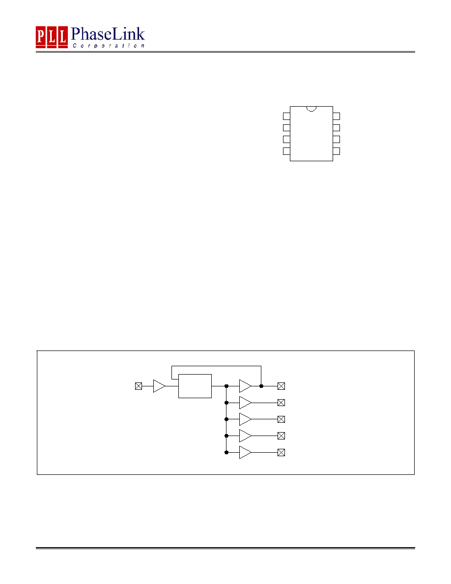
DESCRIPTION
The PLL102-05 is a high performance, low skew, low
jitter zero delay buffer designed to distribute high
speed clocks and is available in 8-pin SOIC package. It
has four outputs that are synchronized with the input.
The synchronization is established via CLKOUT feed
back to the input of the PLL. Since the skew between
the input and output is less than
±350 ps, the device
acts as a zero delay buffer.
PIN CONFIGURATION
Remark
If REF clock is stopped for more than 10us after it has already been
provided to the chip, and after power-up, the output clocks will
disappear. In that instance, a full power-up reset is required in order
to reactivate the output clocks.
BLOCK DIAGRAM
1
2
3
4
REF
5
6
7
8
CLK2
CLK1
GND
CLKOUT
CLK4
VDD
CLK3
PLL 102-05
PLL
REF
CLKOUT
CLK1
CLK2
CLK3
CLK4
PLL102-05
Low Skew Output Buffer
47745 Fremont Blvd., Fremont, California 94538 Tel (510) 492-0990 Fax (510) 492-0991 www.phaselink.com Rev 09/22/05 Page 2
PIN DESCRIPTIONS
Name Number
Type
Description
REF
1
1
I
Input reference frequency. Spread spectrum modulation on this signal will be
passed to the output (up to 100kHz SST modulation).
CLK2
2
2
O
Buffered clock output.
CLK1
2
3
O
Buffered clock output.
GND 4
P
Ground.
CLK3
2
5
O
Buffered clock output.
VDD 6
P
3.3V
Power
Supply.
CLK4
2
7
O
Buffered clock output.
CLKOUT
2
8
O
Buffered clock output. Internal feed back on this pin.
Notes: 1: Weak pull-down. 2: Weak pull-down on all outputs.
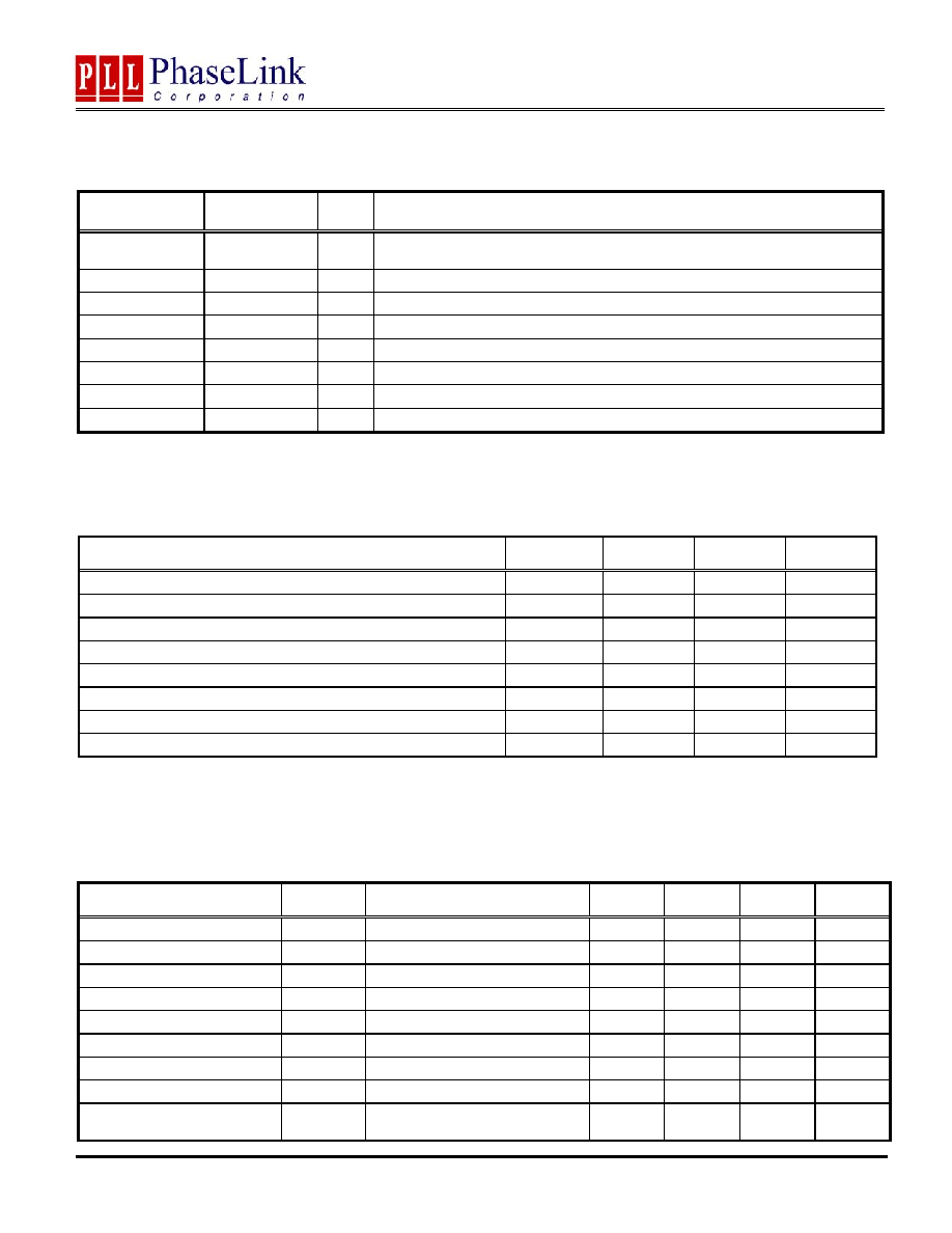
ELECTRICAL SPECIFICATIONS
1. Absolute Maximum Ratings
PARAMETERS SYMBOL
MIN.
MAX.
UNITS
Supply Voltage
V
DD
4.6 V
Input Voltage, dc
V
I
-0.5
V
DD
+0.5 V
Output Voltage, dc
V
O
-0.5
V
DD
+0.5 V
Storage Temperature
T
S
-65 150
∞C
Ambient Operating Temperature*
T
A
-40 85
∞C
Junction Temperature
T
J
125
∞C
Lead Temperature (soldering, 10s)
260
∞C
ESD Protection, Human Body Model
2
kV
Exposure of the device under conditions beyond the limits specified by Maximum Ratings for extended periods may cause permanent damage to the
device and affect product reliability. These conditions represent a stress rating only, and functional operations of the device at these or any other con-
ditions above the operational limits noted in this specification is not implied.
* Note: Operating Temperature is guaranteed by design for all parts (COMMERCIAL and INDUSTRIAL), but tested for COMMERCIAL grade only.
2. Electrical Characteristics
PARAMETERS SYMBOL CONDITIONS
MIN.
TYP.
MAX.
UNITS
Supply Voltage
V
DD
2.97
3.63
V
Input Low Voltage
V
IL
0.8
V
Input High Voltage
V
IH
2.0
V
Input Low Current
I
IL
V
IN
= 0V
19
50.0
µA
Input High Current
I
IH
V
IN
= V
DD
0.10
100.0
µA
Output Low Voltage
V
OL
I
OL
= 50mA
0.25
0.4
V
Output High Voltage
V
OH
I
OH
= 50mA
2.4
2.9
V
Power Down Supply Current
I
DD
REF = 0MHz
0.3
50.0
µA
Supply Current
I
DD
Unloaded outputs at 133MHz,
SEL inputs at V
DD
or GND
35 45
mA
PLL102-05
Low Skew Output Buffer
47745 Fremont Blvd., Fremont, California 94538 Tel (510) 492-0990 Fax (510) 492-0991 www.phaselink.com Rev 09/22/05 Page 3
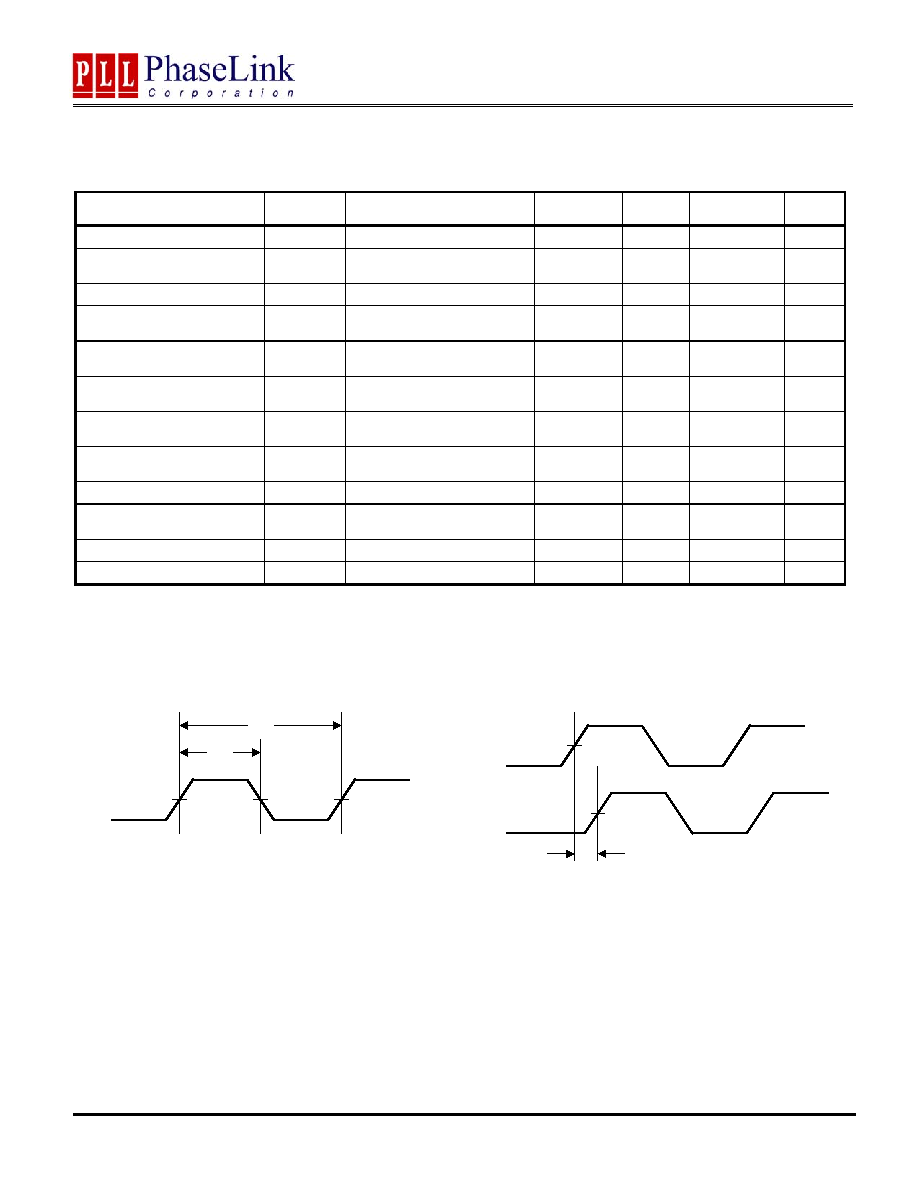
3. Switching Characteristics
PARAMETERS SYMBOL DESCRIPTION MIN.
TYP.
MAX.
UNITS
Output Frequency
t1
25
60
MHz
Duty Cycle ( t2
˜ t1 )
Dt1
Measured at 1.4V,
C
L
=30pF, F
out
= 60MHz
40.0 50.0 60.0 %
Duty Cycle ( t2
˜ t1 )
Dt2
Measured at 1.4V
45.0
50.0
55.0
%
Rise Time
T
r
Measured between 0.8V
and 2.0V, C
L
=30pF
1.2 1.5 ns
Fall Time
T
f
Measured between 2.0V
and 0.8V, C
L
=30pF
1.2 1.5 ns
Output to Output Skew
T
skew
All outputs equally loaded,
C
L
=20pF
250
ps
Delay, REF Rising Edge to
CLKOUT Rising Edge
T
delay
Measured at 1.4V
0
±350
ps
Device to Device Skew
T
dsk-dsk
Measured at V
DD
/2 on the
CLKOUT pins of devices
0 700
ps
Cycle to Cycle Jitter
T
cyc-cyc
Loaded outputs
150
ps
PLL Lock Time
T
lock
Stable power supply, valid
clock presented on REF pin
1.0
ms
Jitter; Absolute Jitter
T
jabs
At 10,000 cycles, C
L
=30pF 70 100 ps
Jitter; 1-sima
T
j1-s
At 10,000 cycles, C
L
=30pF 10 20 ps
SWITCHING WAVEFORMS
Duty Cycle Timing
t1
t2
1.4V
1.4V
1.4V
Output - Output Skew
1.4V
1.4V
T
SKEW
Output
Output
PLL102-05
Low Skew Output Buffer
47745 Fremont Blvd., Fremont, California 94538 Tel (510) 492-0990 Fax (510) 492-0991 www.phaselink.com Rev 09/22/05 Page 4
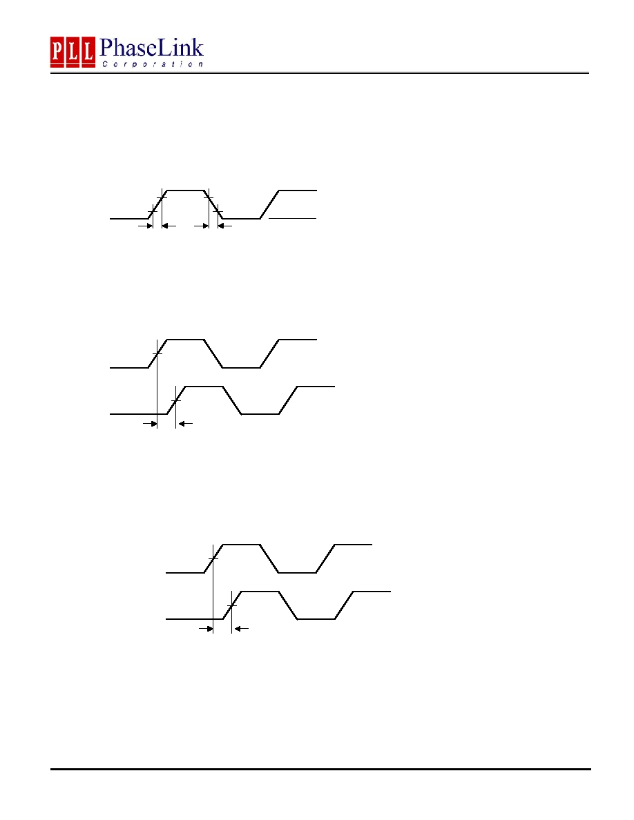
SWITCHING WAVE FORMS
All Outputs Rise/Fall Time
0.8V
2.0V
Output
t
r
t
f
2.0V
0.8V
3.3V
0V
Input to Output Propagation Delay
Input
Output
V
DD
/2
T
delay
V
DD
/2
Device to Device Skew
Device1 CLKOUT
Device2 CLKOUT
V
DD
/2
T
dsk - dsk
V
DD
/2
PLL102-05
Low Skew Output Buffer
47745 Fremont Blvd., Fremont, California 94538 Tel (510) 492-0990 Fax (510) 492-0991 www.phaselink.com Rev 09/22/05 Page 5
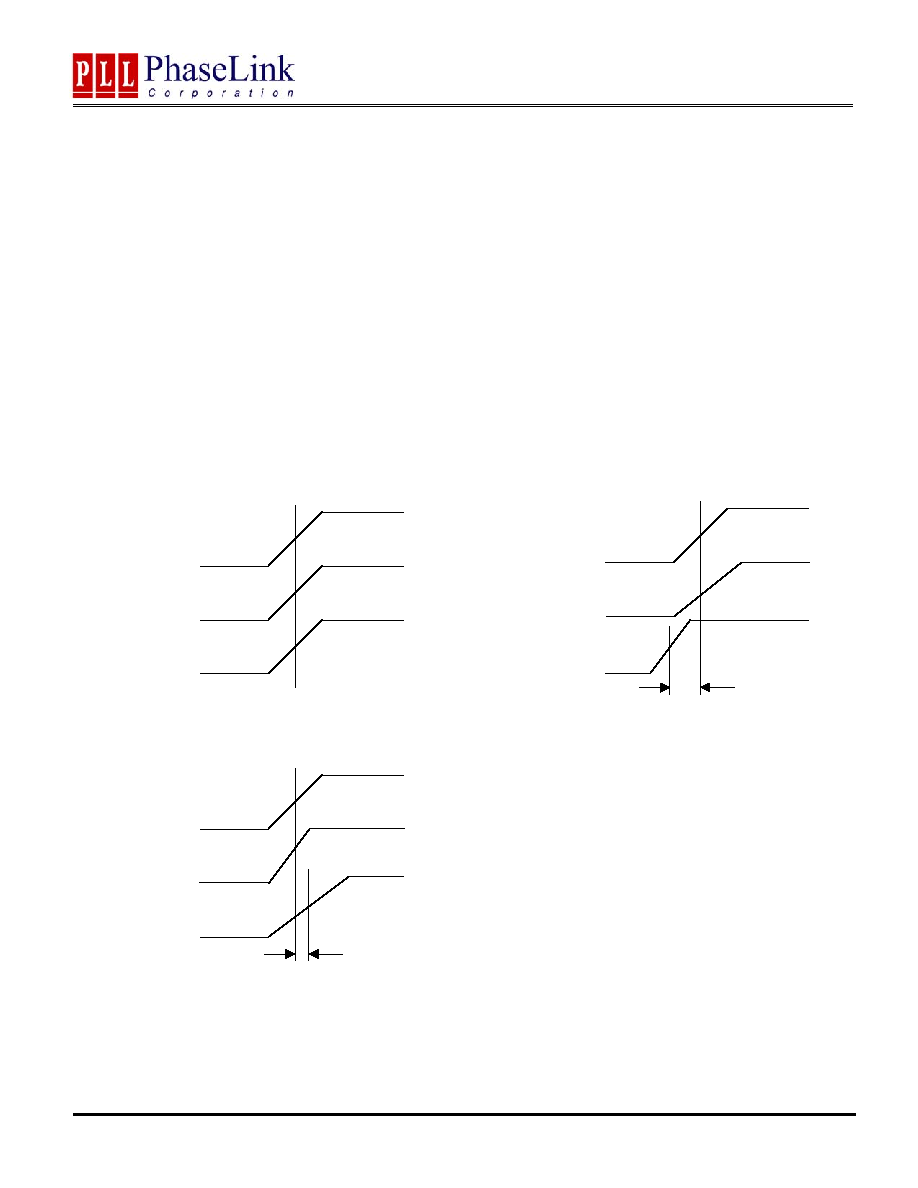
Output-Output Skew
REF
CLKOUT
The skew between CLKOUT and the CLK(1-4) outputs is not dynamically adjusted by the
PLL. Since CLKOUT is one of the inputs to the PLL, zero phase difference is maintained
from REF to CLKOUT. If all outputs are equally loaded, zero phase difference will
maintained from REF to all outputs.
If applications requiring zero output-output skew, all the outputs must equally loaded.
If the CLK(1-4) outputs are less loaded than CLKOUT, CLK(1-4) outputs will lead it; if the
CLK(0-4) is more loaded than CLKOUT, CLK(1-4) will lag the CLKOUT.
Since the CLKOUT and the CLK(1-4) outputs are identical, they all start at the same time,
but difference loads cause them to have different rise times and different times crossing
the measurement thresholds.
CLK(1-4)
Zero Delay
REF
CLKOUT
CLK(1-4)
Advanced
REF
CLKOUT
CLK(1-4)
Delayed
REF input and all outputs loaded equally
REF input and CLK(1-4) outputs loaded equally,
with CLK(1-4) less loaded than CLKOUT.
REF input and CLK(1-4) outputs loaded equally, with
CLK(1-4) more loaded than CLKOUT.