 | ÐлекÑÑоннÑй компоненÑ: PL603-27 | СкаÑаÑÑ:  PDF PDF  ZIP ZIP |
Äîêóìåíòàöèÿ è îïèñàíèÿ www.docs.chipfind.ru

Multimedia Clocks
PL603-27
47745 Fremont Blvd., Fremont, California 94538 TEL (510) 492-0990, FAX (510) 492-0991 Rev.: 07-12-04
Page 1 of 7
Multimedia
Clock
IC
Technical Document
Multimedia Clocks
PL603-27
47745 Fremont Blvd., Fremont, California 94538 TEL (510) 492-0990, FAX (510) 492-0991 Rev.: 07-12-04 Page 2 of 7
PRODUCT DESCRIPTION
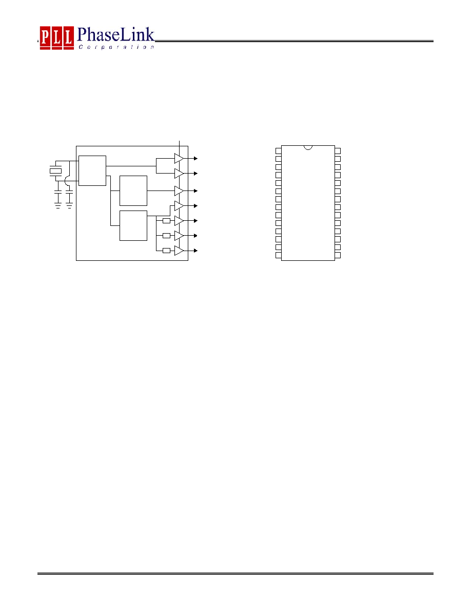
PhaseLink's PL603-27 is a clock generator IC, specifically designed to accommodate the clock requirements of
the set top box, HDTV, and personal video recording (PVR) receiver equipment. It offers seven different clock
signals while utilizing a single low-cost 27MHz crystal input. PhaseLink's PL603-27 is designed to save board
space and implementation cost while producing multiple system clock outputs.
Figure 1: Overall PL603-27 Block Diagram
Figure 2: PL603-27 Pin Assignment
FEATURES
· High accuracy synthesis Phase Locked Loop design
· Eliminates costly quartz crystals and crystal oscillators
· Very low jitter and Phasenoise
· Single 27MHz crystal input
· Seven different output frequencies:
o Two 27MHz output
o One 83.33MHz output
o One 12.288MHz output
o One 3.3864MHz output
o One 1.536MHz output
o One 48KHz output
· OE (output enable) feature
· Low-power sub-micron CMOS process
· Single 3.3V +/- 10% power supply
· Available in 28-pin SSOP package
Xtal
OSC
PLL
PLL
27MHz Xtal
÷
÷
÷
27MHz
48kHz
1.536MHz
3.6864MHz
12.288MHz
83.33MHz
27MHz
OE
P
L603
-
2
7
1
2
3
4
5
6
7
8
9
10
11
12
13
14
15
16
22
23
24
25
26
27
28
21
20
19
18
17
DNC
OE
XOUT
XIN
27MHz
27MHz
83.33MHz
3.6864MHz
12.288MHz
1.536MHz
48KHz
VDD48K
VDDOSC
VDDBUF
VDDBUF
VDD83M
VDD27M
VDDANA
VDDANA
GNDOSC
GNDDIG
GNDBUF
GNDBUF
GND83M
GND27M
GNDANA
GNDANA
GND48K
Multimedia Clocks
PL603-27
47745 Fremont Blvd., Fremont, California 94538 TEL (510) 492-0990, FAX (510) 492-0991 Rev.: 07-12-04 Page 3 of 7
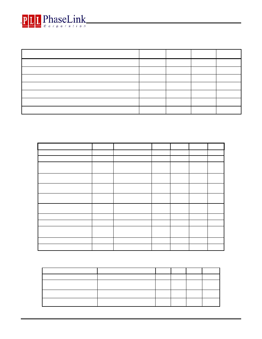
ELECTRICAL SPECIFICATIONS
ABSOLUTE MAXIMUM RATINGS
PARAMETERS SYMBOL
MIN.
MAX.
UNITS
Supply Voltage
V
DD
4.6 V
Input Voltage, dc
V
I
V
SS
-0.5 V
DD
+0.5 V
Output Voltage, dc
V
O
V
SS
-0.5 V
DD
+0.5 V
Storage Temperature
T
S
-55
+150
°C
Ambient Operating Temperature
T
A
-40 +85
°C
Junction Temperature
T
J
125
°C
Lead Temperature (soldering, 10s)
260
°C
Exposure of the device under conditions beyond the limits specified by Maximum Ratings for extended periods may cause permanent damage to the
device and affect product reliability. These conditions represent a stress rating only, and functional operations of the device at these or any other
conditions above the operational limits noted in this specification is not implied.
DC SPECIFICATION
PARAMETERS SYMBOL
CONDITIONS
MIN.
TYP.
MAX.
UNITS
Operating Voltage
VDD
3.13
3.47
V
Input High Voltage
V
IH
VDD/2
V
Input Low Voltage
V
IL
VDD/2
VDD/2
- 1
V
Input High Voltage
V
IH
For all Tri-level
input
VDD-
0.5
V
Input Low Voltage
V
IL
For all Tri-level
input
0.5
V
Input High Voltage
V
IH
For all normal
input
2
V
Input Low Voltage
V
IL
For all normal
input
0.8
V
Output High Voltage
V
OH
I
OH
= -25mA
2.4
V
Output Low Voltage
V
OL
I
OL
= 25mA
0.4
V
Output High Voltage At
CMOS Level
V
OH
I
OH
= -8mA
VDD-
0.4
V
Operating Supply Current
I
DD
No Load
35
mA
Short-circuit Current
I
S
±50
mA
AC SPECIFICATION
PARAMETERS CONDITIONS
MIN.
TYP.
MAX.
UNITS
Input Frequency
27
MHz
Output Clock Rise/Fall Time
10% ~ 90% VDD with 10 pF
load
1.2
1.6
ns
Output Clock Duty Cycle
Measured @ 50% VDD
45
50
55
%
Absolute Short Term Jitter
200
ps
Multimedia Clocks
PL603-27
47745 Fremont Blvd., Fremont, California 94538 TEL (510) 492-0990, FAX (510) 492-0991 Rev.: 07-12-04 Page 4 of 7
PACKAGE PIN DESCRIPTION AND ASSIGNMENT
PIN ASSIGNMENTS
Name
Pin#
Type
Description
XIN
1
I
Input from crystal oscillator circuitry.
GND
2
P
Connect to Ground.
VDD48K
3
P
Connect to 3.3V. Recommend decoupling to GND48K.
48KHz
4
O
48KHz clock output.
VDDANA
5
P
Connect to 3.3V. Recommend decoupling to GNDANA.
VDDANA
6
P
Connect to 3.3V. Recommend decoupling to GNDANA.
VDD27M
7
P
Connect to 3.3V. Recommend decoupling to GND27M.
GND48K
8
P
Connect to Ground.
GNDANA
9
P
Connect to Ground.
GNDANA
10
P
Connect to Ground.
GND27M
11
P
Connect to Ground.
27MHz
12
O
27MHz clock output.
27MHz
13
O
27MHz clock output.
GND83M
14
P
Connect to Ground.
83.33MHZ
15
O
83.33MHz clock output.
VDD83M
16
P
Connect to 3.3V. Recommend decoupling to GND83M.
1,536MHz
17
O
1.536MHz clock output.
3.6864MHZ
18
O
3.6864MHz clock output.
12.288MHz
19
O
12.288MHz clock output.
GNDBUF
20
P
Connect to Ground.
GNDBUF
21
P
Connect to Ground.
GNDOSC
22
P
Connect to Ground.
VDDBUF
23
P
Connect to 3.3V. Recommend decoupling to GNDBUF.
VDDBUF
24
P
Connect to 3.3V. Recommend decoupling to GNDBUF.
DNC
25
N/A Do Not Connect.
OE
26
I
Output Enable.
VDDOSC
27
P
Connect to 3.3V. Recommend decoupling to GNDOSC.
XOUT
28
O
Output from crystal oscillator circuitry.
PL6
03-
27
1
2
3
4
5
6
7
8
9
10
11
12
13
14
15
16
22
23
24
25
26
27
28
21
20
19
18
17
DNC
OE
XOUT
XIN
27MHz
27MHz
83.33MHz
3.6864MHz
12.288MHz
1.536MHz
48KHz
VDD48K
VDDOSC
VDDBUF
VDDBUF
VDD83M
VDD27M
VDDANA
VDDANA
GNDOSC
GNDDIG
GNDBUF
GNDBUF
GND83M
GND27M
GNDANA
GNDANA
GND48K
Multimedia Clocks
PL603-27
47745 Fremont Blvd., Fremont, California 94538 TEL (510) 492-0990, FAX (510) 492-0991 Rev.: 07-12-04 Page 5 of 7
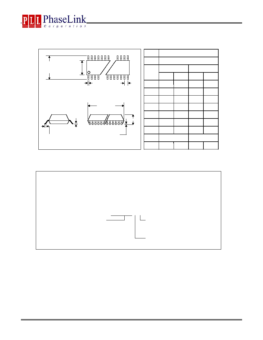
PACKAGE INFORMATION
PART NUMBERING
ORDERING INFORMATION
PhaseLink Corporation, reserves the right to make changes in its products or specifications, or both at any time without
notice. The information furnished by PhaseLink is believed to be accurate and reliable. However, PhaseLink makes no
guarantee or warranty concerning the accuracy of said information and shall not be responsible for any loss or damage of
whatever nature resulting from the use of, or reliance upon this product.
LIFE SUPPORT POLICY
PhaseLink's products are not authorized for use as critical components in life support devices or systems without the
express written approval of the President of PhaseLink Corporation.
A1
D
C
L
A
e
E
E1
B
28PIN SSOP
L
0.022
0.038
0.55
0.95
0.220
e
0.65BSC
0.0256BSC
E1
5.00
5.60
0.197
0.413
E
7.40
8.20
0.291
0.323
D
9.9
10.5
0.390
0.015
C
0.09
0.25
0.004
0.010
B
0.25
0.38
0.01
0.079
A1
0.05
0.002
A
2.0
Unit
mm
inches
min
max
min
max
Package
SSOP (QSOP) 209mil
Pins#
28
For part ordering, please contact our Sales Department:
47745 Fremont Blvd., Fremont, CA 94538, USA
Tel: (510) 492-0990 Fax: (510) 492-0991
PART NUMBER
The order number for this device is a combination of the following:
Device number, Package type and Operating temperature range
PLL603-27 X C
PART NUMBER
TEMPERATURATURE
C=COMMERCIAL
M=MILITARY
I=INDUSTRAL
PACKAGE TYPE
X =SSOP