
PLL102-108
Programmable DDR Zero Delay Clock Driver
47745 Fremont Blvd., Fremont, California 94538 TEL (510) 492-0990 FAX (510) 492-0991 Rev 03/29/02 Page 1
FEATURES
∑
PLL clock distribution optimized for Double Data
Rate SDRAM application up to 266Mhz.
∑
Distributes one clock Input to one bank of ten
differential outputs.
∑
Track spread spectrum clocking for EMI reduction.
∑
Programmable delay between CLK_INT and
CLK[T/C] from ≠0.8ns to +3.1ns by programming
CLKINT and FBOUT skew channel, or from ≠1.1ns to
+3.5ns if additional DDR skew channels are enabled.
∑
Four independent programmable DDR skew chan-
nels from ≠0.3ns to +0.4ns with step size
±
100ps.
∑
Support 2-wire I2C serial bus interface.
∑
2.5V Operating Voltage.
∑
Available in 48-Pin 300mil SSOP.
DESCRIPTIONS
The PLL102-108 is a zero delay buffer that distributes
a single-ended clock input to ten pairs of differential
clock outputs and one feedback clock output. Output
signal duty cycles are adjusted to 50%, independent of
the duty cycle at CLK_INT. The PLL can be bypassed
for test purposes by strapping AV
dd
to ground.
PIN CONFIGURATION
BLOCK DIAGRAM
PLL102-108
CLKT4
CLKT3
CLKC3
GND
AGND
AVDD
VDD
N/C
SCLK
VDD
CLKC2
GND
GND
CLKT1
VDD
CLKT0
CLKC0
GND
GND
CLKC4
VDD
CLKT2
GND
GND
CLKC7
CLKT7
VDD
SDATA
N/C
FB_INT
VDD
FB_OUTT
N/C
GND
CLKC5
CLKT5
VDD
CLKT6
CLKC6
GND
VDD
CLKC8
CLKT8
CLKC9
GND
1
2
3
4
5
6
7
8
9
10
11
12
13
14
15
16
17
18
19
20
21
22
23
24
40
39
38
37
36
35
34
33
32
31
30
29
28
27
26
25
41
42
44
43
45
46
47
48
CLK_INT
CLKC1
CLKT9
CLK_INT
FB_INT
Control
Logic
FB_OUTT
CLKT0
CLKC0
CLKT1
CLKC1
CLKT5
CLKC5
CLKT2
CLKC2
CLKT3
CLKC3
CLKT4
CLKC4
CLKT7
CLKC7
CLKT8
CLKC8
CLKT9
CLKC9
CLKT6
CLKC6
AV
DD
AV
DD
-600~+800ps
±200ps step
-300~+400ps
±100ps step
-300~+400ps
±100ps step
-300~+400ps
±100ps step
-300~+400ps
±100ps step
(0~2.5ns)
+170ps step
PLL
Programmable
Delay Channel
Programmable
Skew Channel

PLL102-108
Programmable DDR Zero Delay Clock Driver
47745 Fremont Blvd., Fremont, California 94538 TEL (510) 492-0990 FAX (510) 492-0991 Rev 03/29/02 Page 2
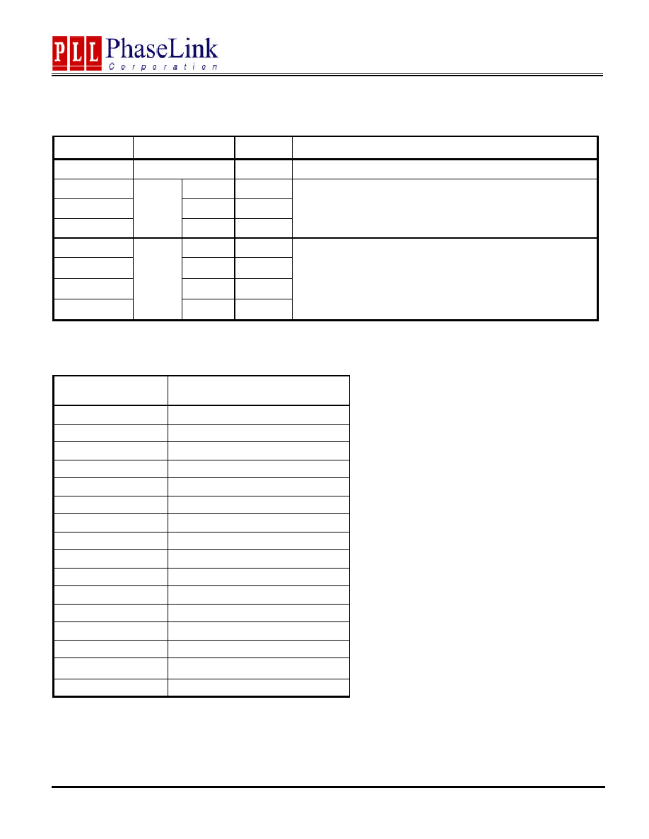
PIN DESCRIPTIONS
Name
Number
Type
Description
VDD
4,11,15,21,28,34,
38,45
P
2.5V power supply.
GND
1,7,8,18,24,
25,31,41,42,48
P
Ground
AVDD
16
P
Analog power supply (2.5V).
AGND
17
P
Analog ground.
CLKT(0:9)
3,5,10,20,22,46,
44,39,29,27
I
"True" clocks of differential pair outputs.
CLKC(0:9)
2,6,9,19,23,47,
43,40,30,26
I
"Complementary" clocks of differential pair outputs.
CLK_INT
13
I
Single-ended 3.3V tolerant input.
N/C
14,32,36
Not connected.
FB_OUTT
33
O
"True" feedback output. Dedicated for external feedback. It switches at the
same frequency as the CLK_INT.
FB_INT
35
I
"True" feedback input, provides feedback signal to the internal PLL for
synchronization with CLK_INT to eliminate phase error.
SDATA
37
B
SCLK
12
I
Serial data input for serial interface port.
Functionality
INPUTS
OUTPUTS
AVDD
CLK_INT
CLK_INC
CLKT
CLKC
FB_OUTT
PLL State
2.5V (Nom)
L
H
L
H
L
On
2.5V (Nom)
H
L
H
L
H
On
GND
L
H
L
H
L
Bypass/Off
GND
H
L
H
L
H
Bypass/Off

PLL102-108
Programmable DDR Zero Delay Clock Driver
47745 Fremont Blvd., Fremont, California 94538 TEL (510) 492-0990 FAX (510) 492-0991 Rev 03/29/02 Page 3
I2C BUS CONFIGURATION SETTING
Address Assignment
A6 A5 A4 A3 A2 A1 A0 R/W
1 1 0 1 0 0 1 _
Slave Re-
ceiver/Transmitter
Provides both slave write and readback functionality
Data Transfer Rate
Standard mode at 100kbits/s
Data Protocol
This serial protocol is designed to allow both blocks write and read from the controller. The
bytes must be accessed in sequential order from lowest to highest byte. Each byte transferred
must be followed by 1 acknowledge bit. A byte transferred without acknowledged bit will termi-
nate the transfer. The write or read block both begins with the master sending a slave address
and a write condition (0xD4) or a read condition (0xD5).
Following the acknowledge of this address byte, in Write Mode: the Command Byte and Byte
Count Byte must be sent by the master but ignored by the slave, in Read Mode: the Byte
Count Byte will be read by the master then all other Data Byte. Byte Count Byte default at
power-up is = (0x09).
I2C CONTROL REGISTERS
1. BYTE 0: Outputs Register (1=Enable, 0=Disable)
Bit
Pin#
Default
Description
Bit 7
39,40
1
CLKT7, CLKC7 (1= active, 0=inactive)
Bit 6
43,44
1
CLKT6, CLKC6 (1= active, 0=inactive)
Bit 5
46,47
1
CLKT5, CLKC5 (1= active, 0=inactive)
Bit 4
22,23
1
CLKT4, CLKC4 (1= active, 0=inactive)
Bit 3
19,20
1
CLKT3, CLKC3 (1= active, 0=inactive)
Bit 2
9,10
1
CLKT2, CLKC2 (1= active, 0=inactive)
Bit 1
5,6
1
CLKT1, CLKC1 (1= active, 0=inactive)
Bit 0
2,3
1
CLKT0, CLKC0 (1= active, 0=inactive)

PLL102-108
Programmable DDR Zero Delay Clock Driver
47745 Fremont Blvd., Fremont, California 94538 TEL (510) 492-0990 FAX (510) 492-0991 Rev 03/29/02 Page 4
TABLE 1: Output Signals SKEW Programming Summary:
Bit<2:0>
DDR Skew Setting (
±
±
100ps/step)
FBOUT Skew Setting (
±
±
200ps/step)
111
+400ps
+800ps
110
+300ps
+600ps
101
+200ps
+400ps
100
+100ps
+200ps
011
Default
Default
010
-100ps
-200ps
001
-200ps
-400ps
000
-300ps
Setting applies to the following
outputs:
1. DDRA: CLK0, CLK1, CLK5
2. DDRB: CLK7, CLK8, CLK9
3. DDRC: CLK2, CLK3, CLK4
4. DDRD: CLK6
-600ps
Setting applies to the following out-
puts:
1. FB_OUTT
2. BYTE 1: SKEW Register (1=Enable, 0=Disable)
Bit
Name
Default
Description
Bit 7
26,27
1
CLKT9, CLKC9 (1= active, 0=inactive)
Bit 6
29,30
1
CLKT8, CLKC8 (1= active, 0=inactive)
Bit 5
Bit <2>
0
Bit 4
Bit <1>
1
Bit 3
Skew
DDRA
Bit <0>
1
These three bits will adjust timing of DDRA signals (CLK0, CLK1,
CLK5) either positive or negative delay up to +400ps or ≠300ps
with
±
100ps per step. (see Table 1)
Bit 2
Bit <2>
0
Bit 1
Bit <1>
1
Bit 0
Skew
DDRB
Bit <0>
1
These three bits will adjust timing of DDRB signals (CLK7, CLK8,
CLK9) either positive or negative delay up to +400ps or ≠300ps
with
±
100ps per step. (see Table 1)
3. BYTE 2: SKEW Register (1=Enable, 0=Disable)
Bit
Name
Default
Description
Bit 7
DDR-SKEWEN
1
1= disable, 0= enable
Bit 6
FBOUT-SKEWEN
1
1= disable, 0= enable
Bit 5
Bit <2>
0
Bit 4
Bit <1>
1
Bit 3
Skew
DDRC
Bit <0>
1
These three bits will adjust timing of DDRC signals (CLK2, CLK3,
CLK4) either positive or negative delay up to +400ps or ≠300ps
with
±
100ps per step. (see Table 1)
Bit 2
Bit <2>
0
Bit 1
Bit <1>
1
Bit 0
Skew
DDRD
Bit <0>
1
These three bits will adjust timing of DDRD signals (CLK6) either
positive or negative delay up to +400ps or ≠300ps with
±
100ps per
step. (see Table 1)
PLL102-108
Programmable DDR Zero Delay Clock Driver
47745 Fremont Blvd., Fremont, California 94538 TEL (510) 492-0990 FAX (510) 492-0991 Rev 03/29/02 Page 5
4. BYTE 3: Outputs Register (1=Enable, 0=Disable)
Bit
Name
Default
Description
Bit 7
-
1
Reserved
Bit 6
Bit <2>
0
Bit 5
Bit <1>
1
Bit 4
Skew
FBOUT
Bit <0>
1
These three bits will adjust timing of FBOUTT signal either positive
or negative delay up to +800ps or ≠600ps with
±
200ps per step.
(see Table 1)
Bit 3
Bit <3>
0
Bit 2
Bit <2>
0
Bit 1
Bit <1>
0
Bit 0
Delay
CLKINT
Bit <0>
0
These four bits will program the propagation delay from CLK_INT
to the input of PLL within the range between 0ps and 2.5ns with
170ps step size. (see Table 2)
TABLE 2: CLK_INT Delay Programming Summary:
Bit<3:0>
CLK_INT to CLK Delay
1111
+2,550 ps
1110
+2,380 ps
1101
+2,210 ps
1100
+2,040 ps
1011
+1,870 ps
1010
+1,700 ps
1001
+1,530 ps
1000
+1,360 ps
0111
+1,190 ps
0110
+1,020 ps
0101
+850 ps
0100
+680 ps
0011
+510 ps
0010
+340 ps
0001
+170 ps
0000
Default