PLL650-09
Low Cost Network LAN Clock
47745 Fremont Blvd., Fremont, California 94538 TEL (510) 492-0990 FAX (510) 492-0991 Rev 09/19/02 Page 1
FEATURES
∑ Full CMOS output swing with 40-mA output drive
capability. 25-mA output drive at TTL level.
∑ Advanced, low power, sub-micron CMOS processes.
∑ 25MHz fundamental crystal or clock input.
∑ 4 outputs fixed at 50MHz .
∑ Zero PPM synthesis error in all clocks.
∑ Ideal for Network switches.
∑ 3.3V operation.
∑
Available in 16-Pin 150mil SOIC
.
DESCRIPTIONS
The PLL 650-09 is a low cost, low jitter, and high
performance clock synthesizer. With PhaseLink's
proprietary analog Phase Locked Loop techniques, the chip
accepts 25.0 MHz crystal, and produces multiple output
clocks for networking chips.
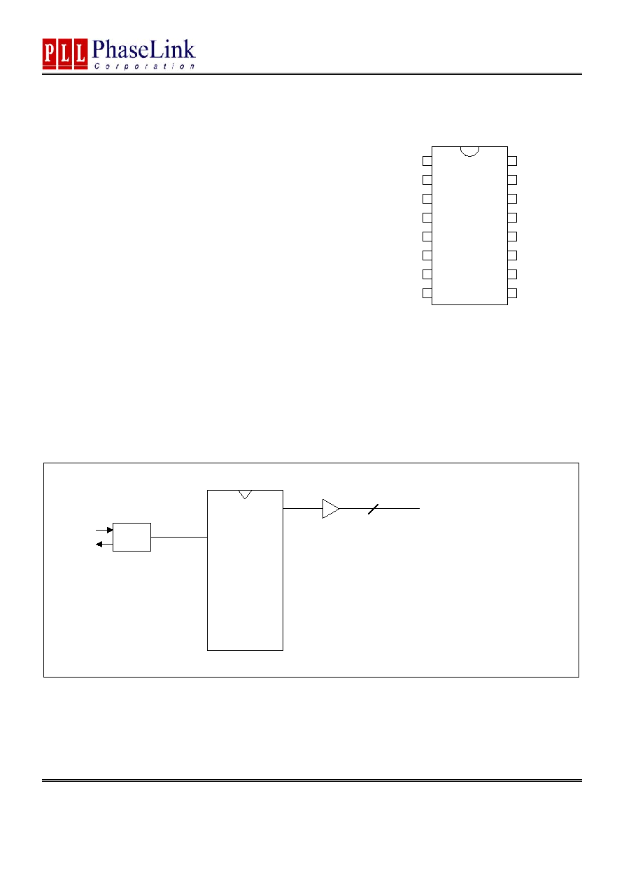
PIN CONFIGURATION
BLOCK DIAGRAM
XTAL
OS C
50MHz
XIN
XOUT
C ontrol
Logic
4
P
L
L
65
0-
09
1
2
3
4
5
6
7
8
9
10
11
12
13
14
15
16
VDD
VDD
N/C
G ND
G ND
GND
VDD
50MHz
XIN
XOUT
G ND
VDD
50MHz
G ND
50MHz
50MHz
PLL650-09
Low Cost Network LAN Clock
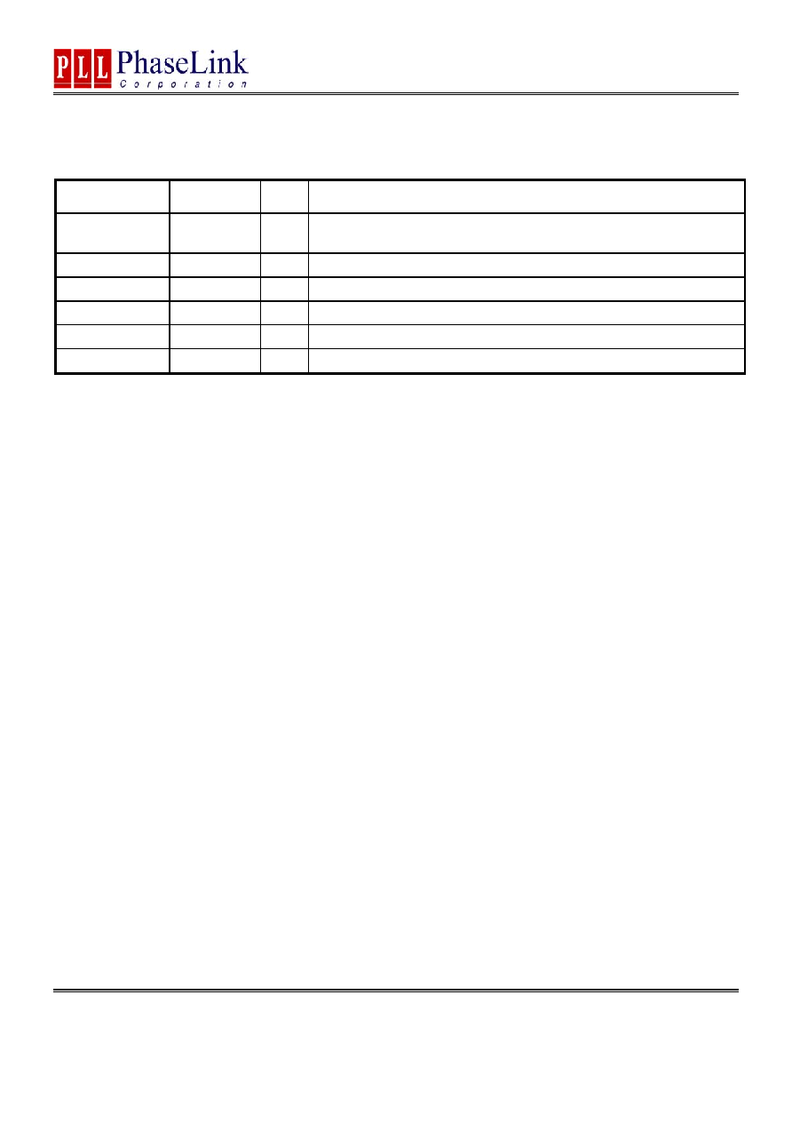
PIN DESCRIPTIONS
Name Number
Type
Description
XIN 1
I
25MHz fundamental crystal input (20pF C
L
parallel resonant). C
L
have been
integrated into the chip. No external C
L
capacitor is required.
XOUT
2
O
Crystal output connection pin.
50MHz 5,7,8,9
O
50MHz
outputs.
N/C 14
-
No
connection.
VDD
4,10,15,16
P
3.3V power supply.
GND 3,6,11,12,13
P
Ground.
47745 Fremont Blvd., Fremont, California 94538 TEL (510) 492-0990 FAX (510) 492-0991 Rev 09/19/02 Page 2
PLL650-09
Low Cost Network LAN Clock
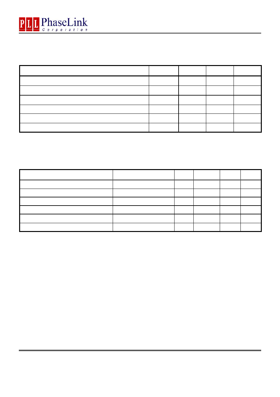
Electrical Specifications
1. Absolute Maximum Ratings
PARAMETERS SYMBOL
MIN.
MAX.
UNITS
Supply Voltage Range
V
CC
-
0.5
7 V
Input Voltage Range
V
I
-
0.5 V
CC
+
0.5
V
Output Voltage Range
V
O
-
0.5 V
CC
+
0.5
V
Soldering Temperature
260
∞C
Storage Temperature
T
S
-65 150
∞C
Ambient Operating Temperature
0
70
∞C
Exposure of the device under conditions beyond the limits specified by Maximum Ratings for extended periods may cause
permanent damage to the device and affect product reliability. These conditions represent a stress rating only, and functional
operations of the device at these or any other conditions above the operational limits noted in this specification is not implied.
2. AC Specification
PARAMETERS CONDITIONS
MIN.
TYP.
MAX.
UNITS
Input Frequency
10
25
27
MHz
Output Rise Time
0.8V to 2.0V with no load
1.5
ns
Output Fall Time
2.0V to 0.8V with no load
1.5
ns
Duty Cycle*
At VDD/2
45
50
55
%
Max. Absolute Jitter
Short term
±150
ps
Max. Jitter, cycle to cycle
80
ps
47745 Fremont Blvd., Fremont, California 94538 TEL (510) 492-0990 FAX (510) 492-0991 Rev 09/19/02 Page 3
PLL650-09
Low Cost Network LAN Clock
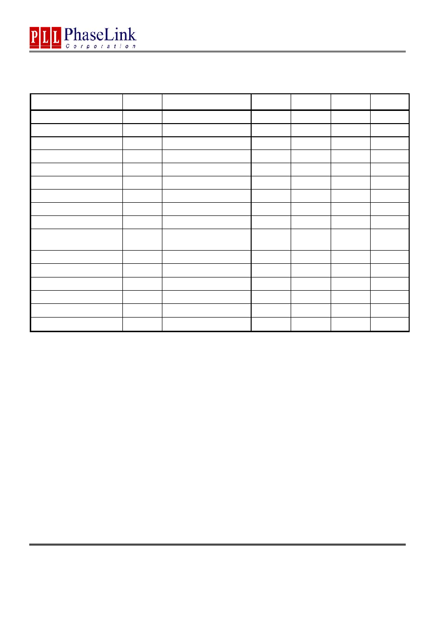
3. DC Specification
PARAMETERS SYMBOL CONDITIONS MIN. TYP. MAX.
UNITS
Operating Voltage
VDD
3.13
3.47
V
Input High Voltage
V
IH
VDD/2 V
Input Low Voltage
V
IL
VDD/2
VDD/2 - 1
V
Input High Voltage
V
IH
For all Tri-level input
VDD-0.5
V
Input Low Voltage
V
IL
For all Tri-level input
0.5
V
Input High Voltage
V
IH
For all normal input
2
V
Input Low Voltage
V
IL
For all normal input
0.8
V
Output High Voltage
V
OH
I
OH
= -25mA
2.4
V
Output Low Voltage
V
OL
I
OL
= 25mA
0.4
V
Output High Voltage At
CMOS Level
V
OH
I
OH
= -8mA
VDD-0.4
V
Operating Supply Current
I
DD
No Load
35
mA
Short-circuit Current
I
S
±100
mA
Nominal output current*
I
out
CMOS output level
35
40
mA
Nominal output current*
I
out
TTL output level
20
25
mA
Internal pull-up resistor
R
up
Pins 5,7
60
k
Internal pull-up resistor
R
up
Pin 2
120
k
47745 Fremont Blvd., Fremont, California 94538 TEL (510) 492-0990 FAX (510) 492-0991 Rev 09/19/02 Page 4
PLL650-09
Low Cost Network LAN Clock
47745 Fremont Blvd., Fremont, California 94538 TEL
PART NUMBER
(510) 492-0990 FAX (510) 492-0991 Rev 09/19/02 Page 5
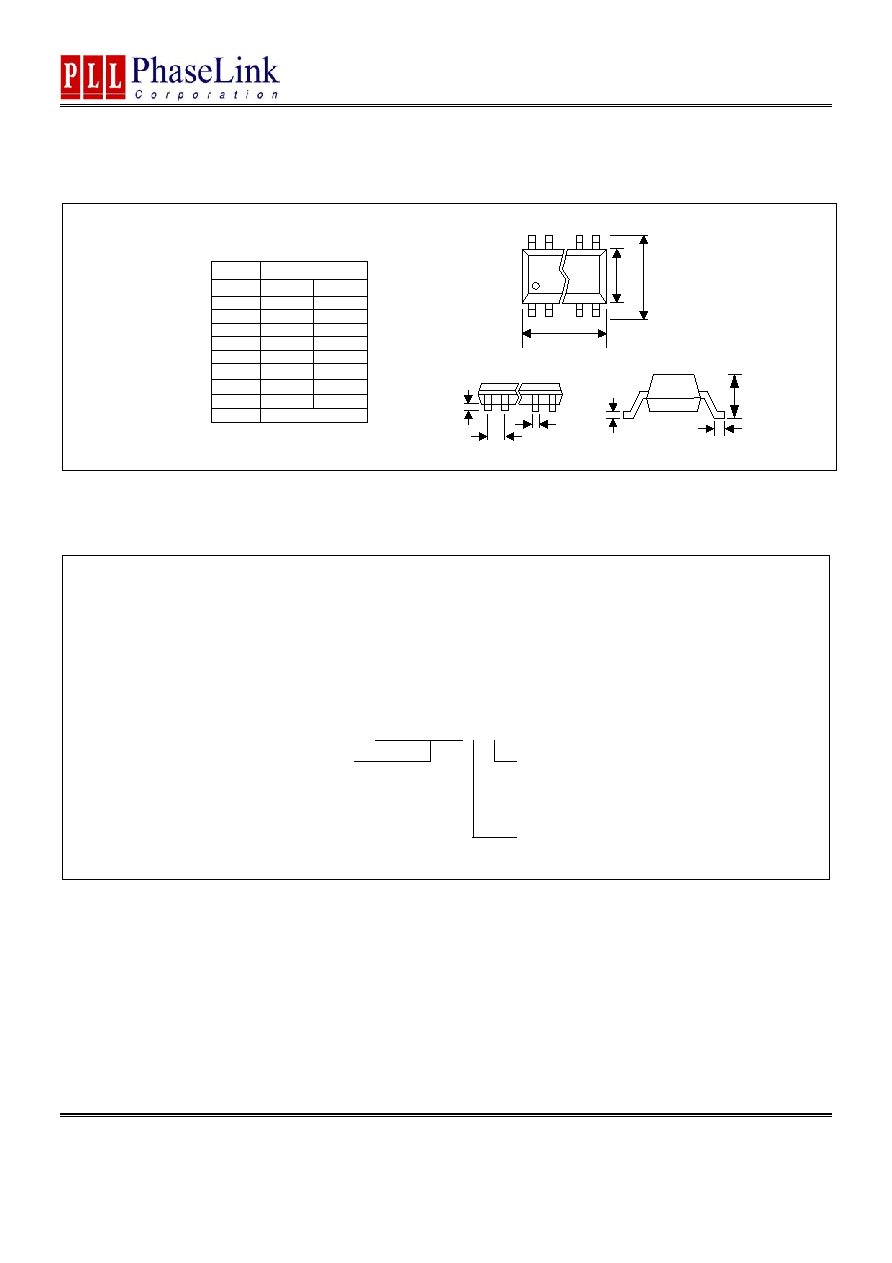
PACKAGE INFORMATION
C
L
A
16 PIN Narrow SOIC ( mm )
SOIC
Symbol
Min.
Max.
A
1.35
1.75
A1
0.10
0.25
B
0.33
0.51
C
0.19
0.25
D
9.80
10.00
E
3.80
4.00
H
5.80
6.20
L
0.40
1.27
e
1.27 BSC
E
H
D
A1
e
B
ORDERING INFORMATION
For part ordering, please contact our Sales Department:
47745 Fremont Blvd., Fremont, CA 94538, USA
Tel: (510) 492-0990 Fax: (510) 492-0991
PART NUMBER
The order number for this device is a combination of the following:
Device number, Package type and Operating temperature range
PLL650-09 S C
TEMPERATURATURE
C=COMMERCIAL
M=MILITARY
I=INDUSTRAL
PACKAGE TYPE
S=SOIC
PhaseLink Corporation, reserves the right to make changes in its products or specifications, or both at any time without notice. The information
furnished by Phaselink is believed to be accurate and reliable. However, PhaseLink makes no guarantee or warranty concerning the accuracy of said
information and shall not be responsible for any loss or damage of whatever nature resulting from the use of, or reliance upon this product.
LIFE SUPPORT POLICY: PhaseLink's products are not authorized for use as critical components in life support devices or systems without the
express written approval of the President of PhaseLink Corporation.