 | –≠–ª–µ–∫—Ç—Ä–æ–Ω–Ω—ã–π –∫–æ–º–ø–æ–Ω–µ–Ω—Ç: PM6388-RI | –°–∫–∞—á–∞—Ç—å:  PDF PDF  ZIP ZIP |

PM6388 EOCTL
DATA SHEET
PMC-1971019
ISSUE 6
OCTAL E1 FRAMER
PROPRIETARY AND CONFIDENTIAL TO PMC-SIERRA INC. AND FOR ITS CUSTOMERS' INTERNAL USE
PM6388
EOCTL
OCTAL E1 FRAMER
DATA SHEET
ISSUE 6: JANUARY, 2000

PM6388 EOCTL
DATA SHEET
PMC-1971019
ISSUE 6
OCTAL E1 FRAMER
PROPRIETARY and CONFIDENTIAL to PMC-Sierra Inc. and for its customers' internal use
i
CONTENTS
1
FEATURES .............................................................................................. 1
2
APPLICATIONS ....................................................................................... 4
3
REFERENCES......................................................................................... 5
4
APPLICATION EXAMPLES ..................................................................... 7
5
BLOCK DIAGRAM ................................................................................... 8
6
DESCRIPTION ........................................................................................ 9
7
PIN DIAGRAM ........................................................................................11
8
PIN DESCRIPTION................................................................................ 12
9
FUNCTIONAL DESCRIPTION............................................................... 24
9.1
E1 FRAMER (E1-FRMR)............................................................. 24
9.2
PERFORMANCE MONITOR COUNTERS (PMON) ................... 30
9.3
DATA LINK EXTRACTOR (RXCE) .............................................. 31
9.4
HDLC RECEIVER (RDLC) .......................................................... 31
9.5
ELASTIC STORE (ELST)............................................................ 32
9.6
SIGNALING EXTRACTOR (SIGX).............................................. 32
9.7
RECEIVE PER-CHANNEL SERIAL CONTROLLER (RPSC)...... 33
9.8
PATTERN DETECTOR/GENERATOR (PRGD) .......................... 33
9.9
E1 TRANSMITTER (E1-TRAN)................................................... 34
9.10 TRANSMIT PER-CHANNEL SERIAL CONTROLLER (TPSC).... 34
9.11 TRANSMIT DATA LINK INSERTER (TXCI)................................. 35
9.12 FACILITY DATA LINK TRANSMITTER (TDPR) .......................... 35
9.13 RECEIVE AND TRANSMIT DIGITAL JITTER ATTENUATOR (RJAT,
TJAT)........................................................................................... 36

PM6388 EOCTL
DATA SHEET
PMC-1971019
ISSUE 6
OCTAL E1 FRAMER
PROPRIETARY and CONFIDENTIAL to PMC-Sierra Inc. and for its customers' internal use
ii
9.14 TIMING OPTIONS (TOPS) ......................................................... 40
9.15 BACKPLANE RECEIVE INTERFACE (BRIF) ............................. 40
9.15.1
NON-MULTIPLEXED BUS INGRESS MODES............. 40
9.15.2
MULTIPLEXED BUS INGRESS MODE ........................ 42
9.16 BACKPLANE TRANSMIT INTERFACE (BTIF) ........................... 43
9.16.1
NON-MULTIPLEXED BUS EGRESS MODES.............. 43
9.16.2
MULTIPLEXED EGRESS INTERFACE ........................ 45
9.17 JTAG TEST ACCESS PORT....................................................... 46
9.18 MICROPROCESSOR INTERFACE ............................................ 46
10
NORMAL MODE REGISTER DESCRIPTION ....................................... 52
11
OPERATION ........................................................................................ 255
11.1 CONFIGURING THE EOCTL FROM RESET ........................... 255
11.2 USING THE MULTIPLEXED BACKPLANE............................... 263
11.2.1
INGRESS MULTIPLEXED BUS CONFIGURATION ... 263
11.2.2
EGRESS MULTIPLEXED BUS CONFIGURATION .... 264
11.3 USING THE PER-TIMESLOT TRANSMIT DATA LINK DIRECTOR
.................................................................................................. 266
11.4 USING THE INTERNAL FDL TRANSMITTER .......................... 267
11.5 USING THE PER-TIMESLOT RECEIVE DATA LINK EXTRACTOR
.................................................................................................. 270
11.6 USING THE INTERNAL FDL RECEIVER ................................. 271
11.7 USING THE PRGD PATTERN GENERATOR/DETECTOR ...... 275
11.8 USING THE LOOPBACK MODES ............................................ 280
11.8.1
LINE LOOPBACK ....................................................... 280
11.8.2
DIAGNOSTIC DIGITAL LOOPBACK .......................... 280

PM6388 EOCTL
DATA SHEET
PMC-1971019
ISSUE 6
OCTAL E1 FRAMER
PROPRIETARY and CONFIDENTIAL to PMC-Sierra Inc. and for its customers' internal use
iii
11.8.3
PER-TS LOOPBACK .................................................. 281
11.9 USING THE PER-TS SERIAL CONTROLLERS ....................... 283
11.9.1
INITIALIZATION.......................................................... 283
11.9.2
DIRECT ACCESS MODE ........................................... 283
11.9.3
INDIRECT ACCESS MODE ........................................ 283
11.10 USING THE TRANSMIT DIGITAL JITTER ATTENUATOR ....... 284
11.10.1 DEFAULT APPLICATION............................................ 284
11.10.2 DATA BURST APPLICATION...................................... 285
11.10.3 ELASTIC STORE APPLICATION ............................... 285
11.10.4 ALTERNATE TLCLK REFERENCE APPLICATION.... 286
11.11 ISOLATING AN INTERRUPT .................................................... 286
11.12 USING THE PERFORMANCE MONITOR COUNTER VALUES286
11.13 JTAG SUPPORT ....................................................................... 289
12
FUNCTIONAL TIMING......................................................................... 294
13
ABSOLUTE MAXIMUM RATINGS ....................................................... 302
14
D .C. CHARACTERISTICS ................................................................. 303
15
MICROPROCESSOR INTERFACE TIMING CHARACTERISTICS..... 305
16
EOCTL I/O TIMING CHARACTERISTICS ........................................... 310
17
ORDERING AND THERMAL INFORMATION...................................... 322
18
MECHANICAL INFORMATION............................................................ 323

PM6388 EOCTL
DATA SHEET
PMC-1971019
ISSUE 6
OCTAL E1 FRAMER
PROPRIETARY and CONFIDENTIAL to PMC-Sierra Inc. and for its customers' internal use
iv
LIST OF REGISTERS
REGISTERS 000H, 080H, 100H, 180H, 200H, 280H, 300H, 380H: RECEIVE
LINE OPTIONS................................................................................................. 53
REGISTERS 001H, 081H, 101H, 181H, 201H, 281H, 301H, 381H: INGRESS
INTERFACE OPTIONS .................................................................................... 56
REGISTERS 002H, 082H, 102H, 182H, 202H, 282H, 302H. 382H: TRANSMIT
INTERFACE CONFIGURATION....................................................................... 59
REGISTERS 003H, 083H, 103H, 183H, 203H, 283H, 303H, 383H: EGRESS
INTERFACE OPTIONS .................................................................................... 61
REGISTERS 004H, 084H, 104H, 184H, 204H, 284H, 304H, 384H: TRANSMIT
TIMING OPTIONS ............................................................................................ 63
REGISTERS 005H, 085H, 105H, 185H, 205H, 285H, 305H, 385H: INTERRUPT
SOURCE #1 69
REGISTERS 006H, 086H, 106H, 186H, 206H, 286H, 306H, 386H: INTERRUPT
SOURCE #2 70
REGISTERS 007H, 087H, 107H, 187H, 207H, 287H, 307H, 387H:
DIAGNOSTICS ................................................................................................. 71
REGISTER 008H: EOCTL MASTER TEST...................................................... 73
REGISTER 009H: EOCTL REVISION/CHIP ID/GLOBAL PMON UPDATE...... 75
REGISTERS 00AH, 08AH, 10AH, 18AH, 20AH, 28AH, 30AH, 38AH: DATA LINK
MICRO SELECT/FRAMER RESET.................................................................. 76
REGISTER 00BH: INTERRUPT ID .................................................................. 78
REGISTERS 00CH, 08CH, 10CH, 18CH, 20CH, 28CH, 30CH, 38CH: PATTERN
GENERATOR/DETECTOR POSITIONING/CONTROL.................................... 79
REGISTERS 00DH, 08DH, 10DH, 18DH, 20DH, 28DH, 30DH, 38DH: CLOCK
MONITOR
81
REGISTERS 00EH, 08EH, 10EH, 18EH, 20EH, 28EH, 30EH, 38EH: INGRESS
FRAME PULSE CONFIGURATION.................................................................. 83

PM6388 EOCTL
DATA SHEET
PMC-1971019
ISSUE 6
OCTAL E1 FRAMER
PROPRIETARY and CONFIDENTIAL to PMC-Sierra Inc. and for its customers' internal use
v
REGISTERS 010H, 090H, 110H, 190H, 210H, 290H, 310H, 390H: RECEIVE
BACKPLANE CONFIGURATION ..................................................................... 85
REGISTERS 011H, 091H, 111H, 191H, 211H, 291H, 311H, 391H: RECEIVE
BACKPLANE FRAME PULSE CONFIGURATION ........................................... 88
REGISTERS 012H, 092H, 112H, 192H, 212H, 292H, 312H, 392H: RECEIVE
BACKPLANE PARITY/F-BIT CONFIGURATION.............................................. 92
REGISTERS 013H, 093H, 113H, 193H, 213H, 293H, 313H, 393H: RECEIVE
BACKPLANE TIME SLOT OFFSET ................................................................. 94
REGISTERS 014H, 094H, 114H, 194H, 214H, 294H, 314H, 394H: RECEIVE
BACKPLANE BIT OFFSET .............................................................................. 95
REGISTERS 018H, 098H, 118H, 198H, 218H, 298H, 318H, 398H: TRANSMIT
BACKPLANE CONFIGURATION ..................................................................... 97
REGISTERS 019H, 099H, 119H, 199H, 219H, 299H, 319H, 399H: TRANSMIT
BACKPLANE FRAME PULSE CONFIGURATION ......................................... 100
REGISTERS 01AH, 09AH, 11AH, 19AH, 21AH, 29AH, 31AH, 39AH: TRANSMIT
BACKPLANE PARITY CONFIGURATION AND STATUS............................... 101
REGISTERS 01BH, 09BH, 11BH, 19BH, 21BH, 29BH, 31BH, 39BH: TRANSMIT
BACKPLANE TIME SLOT OFFSET ............................................................... 103
REGISTERS 01CH, 09CH, 11CH, 19CH, 21CH, 29CH, 31CH, 39CH:
TRANSMIT BACKPLANE BIT OFFSET ......................................................... 104
REGISTERS 020H, 0A0H, 120H, 1A0H, 220H, 2A0H, 320H, 3A0H: RJAT
INTERRUPT STATUS..................................................................................... 106
REGISTER 021H, 0A1H, 121H, 1A1H, 221H, 2A1H, 321H, 3A1H: RJAT
REFERENCE CLOCK DIVISOR (N1) CONTROL .......................................... 107
REGISTERS 022H, 0A2H, 122H, 1A2H, 222H, 2A2H, 322H, 3A2H: RJAT
OUTPUT CLOCK DIVISOR (N2) CONTROL.................................................. 108
REGISTERS 023H, 0A3H, 123H, 1A3H, 223H, 2A3H, 323H, 3A3H: RJAT
CONFIGURATION.......................................................................................... 109
REGISTERS 024H, 0A4H, 124H, 1A4H, 224H, 2A4H, 324H, 3A4H: TJAT
INTERRUPT STATUS...................................................................................... 111

PM6388 EOCTL
DATA SHEET
PMC-1971019
ISSUE 6
OCTAL E1 FRAMER
PROPRIETARY and CONFIDENTIAL to PMC-Sierra Inc. and for its customers' internal use
vi
REGISTER 025H, 0A5H, 125H, 1A5H, 225H, 2A5H, 325H, 3A5H: TJAT
REFERENCE CLOCK DIVISOR (N1) CONTROL ...........................................112
REGISTERS 026H, 0A6H, 126H, 1A6H, 226H, 2A6H, 326H, 3A6H: TJAT
OUTPUT CLOCK DIVISOR (N2) CONTROL...................................................113
REGISTERS 027H, 0A7H, 127H, 1A7H, 227H, 2A7H, 327H, 3A7H: TJAT
CONFIGURATION...........................................................................................114
REGISTERS 028H, 0A8H, 128H, 1A8H, 228H, 2A8H, 328H, 3A8H (TXCISEL =
0): RXCE RECEIVE DATA LINK 1 CONTROL.................................................116
REGISTERS 029H, 0A9H, 129H, 1A9H, 229H, 2A9H, 329H, 3A9H (TXCISEL =
0): RXCE DATA LINK 1 BIT SELECT REGISTER ...........................................118
REGISTERS 02AH, 0AAH, 12AH, 1AAH, 22AH, 2AAH, 32AH, 3AAH (TXCISEL
= 0): RXCE RECEIVE DATA LINK 2 CONTROL .............................................119
REGISTERS 02BH, 0ABH, 12BH, 1ABH, 22BH, 2ABH, 32BH, 3ABH (TXCISEL
= 0): RXCE DATA LINK 2 BIT SELECT REGISTER ....................................... 120
REGISTERS 02CH, 0ACH, 12CH, 1ACH, 22CH, 2ACH, 32CH, 3ACH (TXCISEL
= 0): RXCE RECEIVE DATA LINK 3 CONTROL ............................................ 121
REGISTERS 02DH, 0ADH, 12DH, 1ADH, 22DH, 2ADH, 32DH, 3ADH (TXCISEL
= 0): RXCE DATA LINK 3 BIT SELECT REGISTER ....................................... 122
REGISTER 028H, 0A8H, 128H, 1A8H, 228H, 2A8H, 328H, 3A8H (TXCISEL =
1): TXCI TRANSMIT DATA LINK 1 CONTROL ............................................... 123
REGISTERS 029H, 0A9H, 129H, 1A9H, 229H, 2A9H, 329H, 3A9H (TXCISEL =
1): TXCI DATA LINK 1 BIT SELECT REGISTER............................................ 125
REGISTER 02AH, 0AAH, 12AH, 1AAH, 22AH, 2AAH, 32AH, 3AAH (TXCISEL =
1): TXCI TRANSMIT DATA LINK 2 CONTROL ............................................... 126
REGISTERS 02BH, 0ABH, 12BH, 1ABH, 22BH, 2ABH, 32BH, 3ABH (TXCISEL
= 1): TXCI DATA LINK 2 BIT SELECT REGISTER......................................... 128
REGISTER 02CH, 0ACH, 12CH, 1ACH, 22CH, 2ACH, 32CH, 3ACH (TXCISEL =
1): TXCI TRANSMIT DATA LINK 3 CONTROL ............................................... 131
REGISTERS 02DH, 0ADH, 12DH, 1ADH, 22DH, 2ADH, 32DH, 3ADH (TXCISEL
= 1): TXCI DATA LINK 3 BIT SELECT REGISTER......................................... 133

PM6388 EOCTL
DATA SHEET
PMC-1971019
ISSUE 6
OCTAL E1 FRAMER
PROPRIETARY and CONFIDENTIAL to PMC-Sierra Inc. and for its customers' internal use
vii
REGISTERS 030H, 0B0H, 130H, 1B0H, 230H, 2B0H, 330H, 3B0H: E1 FRMR
FRAME ALIGNMENT OPTIONS .................................................................... 134
REGISTERS 031H, 0B1H, 131H, 1B1H, 231H, 2B1H, 331H, 3B1H: E1 FRMR
MAINTENANCE MODE OPTIONS................................................................. 136
REGISTERS 032H, 0B2H, 132H, 1B2H, 232H, 2B2H, 332H, 3B2H: E1 FRMR
FRAMING STATUS INTERRUPT ENABLE .................................................... 138
REGISTERS 033H, 0B3H, 133H, 1B3H, 233H, 2B3H, 333H, 3B3H: E1 FRMR
MAINTENANCE/ALARM STATUS INTERRUPT ENABLE ............................. 139
REGISTERS 034H, 0B4H, 134H, 1B4H, 234H, 2B4H, 334H, 3B1H: E1 FRMR
FRAMING STATUS INTERRUPT INDICATION.............................................. 140
REGISTERS 035H, 0B5H, 135H, 1B5H, 235H, 2B5H, 335H, 3B5H: E1 FRMR
MAINTENANCE/ALARM STATUS INTERRUPT INDICATION....................... 141
REGISTERS 036H, 0B6H, 136H, 1B6H, 236H, 2B6H, 336H, 3B6H: E1 FRMR
FRAMING STATUS......................................................................................... 142
REGISTERS 037H, 0B7H, 137H, 1B7H, 237H, 2B7H, 337H, 3B7H: E1 FRMR
MAINTENANCE/ALARM STATUS.................................................................. 144
REGISTERS 038H, 0B8H, 138H, 1B8H, 238H, 2B8H, 338H, 3B8H: E1 FRMR
TIMESLOT 0 INTERNATIONAL/NATIONAL BITS.......................................... 146
REGISTERS 039H, 0B9H, 139H, 1B9H, 239H, 2B9H, 339H, 3B9H: E1 FRMR
CRC ERROR COUNTER ≠ LSB..................................................................... 148
REGISTERS 03AH, 0BAH, 13AH, 1BAH, 23AH, 2BAH, 33AH, 3BAH: E1 FRMR
CRC ERROR COUNTER ≠ MSB/TIMESLOT 16 EXTRA BITS ...................... 149
REGISTERS 03BH, 0BBH, 13BH, 1BBH, 23BH, 2BBH, 33BH, 3BBH: E1 FRMR
NATIONAL BIT CODEWORD INTERRUPT ENABLES.................................. 151
REGISTERS 03CH, 0BCH, 13CH, 1BCH, 23CH, 2BCH, 33CH, 3BCH: E1 FRMR
NATIONAL BIT CODEWORD INTERRUPTS ................................................. 153
REGISTERS 03DH, 0BDH, 13DH, 1BDH, 23DH, 2BDH, 33DH, 3BDH: E1 FRMR
NATIONAL BIT CODEWORD......................................................................... 154
REGISTERS 03EH, 0BEH, 13EH, 1BEH, 23EH, 2BEH, 33EH, 3BEH: E1 FRMR
FRAME PULSE/ALARM/V5.2 LINK ID INTERRUPT ENABLES .................... 155

PM6388 EOCTL
DATA SHEET
PMC-1971019
ISSUE 6
OCTAL E1 FRAMER
PROPRIETARY and CONFIDENTIAL to PMC-Sierra Inc. and for its customers' internal use
viii
REGISTERS 03FH, 0BFH, 13FH, 1BFH, 23FH, 2BFH, 33FH, 3BFH: E1 FRMR
FRAME PULSE/ALARM INTERRUPTS ......................................................... 157
REGISTERS 040H, 0C0H, 140H, 1C0H, 240H, 2C0H, 340H, 3C0H: E1 TRAN
CONFIGURATION.......................................................................................... 159
REGISTERS 041H, 0C1H, 141H, 1C1H, 241H, 2C1H, 341H, 3C1H: E1 TRAN
TRANSMIT ALARM/DIAGNOSTIC CONTROL............................................... 163
REGISTERS 042H, 0C2H, 142H, 1C2H, 242H, 2C2H, 342H, 3C2H: E1 TRAN
INTERNATIONAL BITS CONTROL................................................................ 165
REGISTERS 043H, 0C3H, 143H, 1C3H, 243H, 2C3H, 343H, 3C3H: E1 TRAN
EXTRA BITS CONTROL ................................................................................ 166
REGISTERS 044H, 0C4H, 144H, 1C4H, 244H, 2C4H, 344H, 3C4H: E1 TRAN
INTERRUPT ENABLE REGISTER................................................................. 167
REGISTERS 045H, 0C5H, 145H, 1C5H, 245H, 2C5H, 345H, 3C5H: E1 TRAN
INTERRUPT STATUS REGISTER ................................................................. 168
REGISTERS 046H, 0C6H, 146H, 1C6H, 246H, 2C6H, 346H, 3C6H: E1 TRAN
NATIONAL BIT CODEWORD SELECT.......................................................... 169
REGISTERS 047H, 0C7H, 147H, 1C7H, 247H, 2C7H, 347H, 3C7H: E1 TRAN
NATIONAL BIT CODEWORD......................................................................... 171
REGISTERS 048H, 0C8H, 148H, 1C8H, 248H, 2C8H, 348H, 3C8H: RDLC #1,
#2, #3 CONFIGURATION............................................................................... 172
REGISTERS 049H, 0C9H, 149H, 1C9H, 249H, 2C9H, 349H, 3C9H: RDLC #1,
#2, #3 INTERRUPT CONTROL...................................................................... 174
REGISTERS 04AH, 0CAH, 14AH, 1CAH, 24AH, 2CAH, 34AH, 3CAH: RDLC#1,
#2, #3 STATUS ............................................................................................... 175
REGISTERS 04BH, 0CBH, 14BH, 1CBH, 24BH, 2CBH, 34BH, 3CBH: RDLC #1,
#2, #3 DATA 178
REGISTERS 04CH, 0CCH, 14CH, 1CCH, 24CH, 2CCH, 34CH, 3CCH: RDLC
#1, #2, #3 PRIMARY ADDRESS MATCH ....................................................... 179
REGISTERS 04DH, 0CDH, 14DH, 1CDH, 24DH, 2CDH, 34DH, 3CDH: RDLC
#1, #2, #3 SECONDARY ADDRESS MATCH................................................. 180

PM6388 EOCTL
DATA SHEET
PMC-1971019
ISSUE 6
OCTAL E1 FRAMER
PROPRIETARY and CONFIDENTIAL to PMC-Sierra Inc. and for its customers' internal use
ix
REGISTER 050H, 0D0H, 150H, 1D0H, 250H, 2D0H ,350H, 3D0H: TDPR #1,
#2, #3 CONFIGURATION............................................................................... 181
REGISTER 051H, 0D1H, 151H, 1D1H, 251H, 2D1H ,351H, 3D1H: TDPR #1,
#2, #3 UPPER TRANSMIT THRESHOLD ...................................................... 183
REGISTER 052H, 0D2H, 152H, 1D2H, 252H, 2D2H ,352H, 3D2H: TDPR #1,
#2, #3LOWER INTERRUPT THRESHOLD .................................................... 184
REGISTER 053H, 0D3H, 153H, 1D3H, 253H, 2D3H ,353H, 3D3H: TDPR #1,
#2, #3 INTERRUPT ENABLE ......................................................................... 185
REGISTER 054H, 0D4H, 154H, 1D4H, 254H, 2D4H ,354H, 3D4H: TDPR #1,
#2, #3 INTERRUPT STATUS/UDR CLEAR.................................................... 187
REGISTER 055H, 0D5H, 155H, 1D5H, 255H, 2D5H ,355H, 3D5H: TDPR #1,
#2, #3 TRANSMIT DATA ................................................................................ 189
REGISTERS 058H, 0D8H, 158H, 1D8H, 258H, 2D8H, 358H, 3D8H: ELST
CONFIGURATION.......................................................................................... 190
REGISTERS 059H, 0D9H, 159H, 1D9H, 259H, 2D9H, 359H, 3D9H: ELST
INTERRUPT ENABLE/STATUS ..................................................................... 191
REGISTERS 05AH, 0DAH, 15AH, 1DAH, 25AH, 2DAH, 35AH, 3DAH: ELST
IDLE CODE 192
REGISTER 05CH, 0DCH, 15CH, 1DCH, 25CH, 2DCH ,35CH, 3DCH: RPSC
CONFIGURATION.......................................................................................... 193
REGISTER 05DH, 0DDH, 15DH, 1DDH, 25DH, 2DDH ,35DH, 3DDH: RPSC µP
ACCESS STATUS .......................................................................................... 194
REGISTER 05EH, 0DEH, 15EH, 1DEH, 25EH, 2DEH ,35EH, 3DEH: RPSC
CHANNEL INDIRECT ADDRESS/CONTROL ................................................ 195
REGISTER 05FH, 0DFH, 15FH, 1DFH, 25FH, 2DFH ,35FH, 3DAH: RPSC
CHANNEL INDIRECT DATA BUFFER............................................................ 196
REGISTER 060H, 0E0H, 160H, 1E0H, 260H, 2E0H ,360H, 3E0H: TPSC
CONFIGURATION.......................................................................................... 203
REGISTER 061H, 0E1H, 161H, 1E1H, 261H, 2E1H ,361H, 3E1H: TPSC µP
ACCESS STATUS .......................................................................................... 204

PM6388 EOCTL
DATA SHEET
PMC-1971019
ISSUE 6
OCTAL E1 FRAMER
PROPRIETARY and CONFIDENTIAL to PMC-Sierra Inc. and for its customers' internal use
x
REGISTER 062H, 0E2H, 162H, 1E2H, 262H, 2E2H ,362H, 3E2H: TPSC
CHANNEL INDIRECT ADDRESS/CONTROL ................................................ 205
REGISTER 063H, 0E3H, 163H, 1E3H, 263H, 2E3H ,363H, 3E3H: TPSC
CHANNEL INDIRECT DATA BUFFER............................................................ 206
REGISTER 064H, 0E4H, 164H, 1E4H, 264H, 2E4H ,364H, 3E4H: SIGX
CONFIGURATION REGISTER (COSS = 0) ................................................... 213
REGISTER 064H, 0E4H, 164H, 1E4H, 264H, 2E4H ,364H, 3E4H: SIGX
CHANGE OF SIGNALING STATE REGISTER (COSS = 1)........................... 215
REGISTER 065H, 0E5H, 165H, 1E5H, 265H, 2E5H ,365H, 3E5H: SIGX
TIMESLOT INDIRECT STATUS (COSS = 0).................................................. 216
REGISTER 065H, 0E5H, 165H, 1E5H, 265H, 2E5H ,365H, 3E5H: SIGX
CHANGE OF SIGNALING STATE CHANGE (COSS=1) ................................ 217
REGISTER 066H, 0E6H, 166H, 1E6H, 266H, 2E6H ,366H, 3E6H: SIGX
TIMESLOT INDIRECT ADDRESS/CONTROL (COSS = 0) ............................ 218
REGISTER 066H, 0E6H, 166H, 1E6H, 266H, 2E6H ,366H, 3E6H: SIGX
CHANGE OF SIGNALING STATE REGISTER (COSS = 1)........................... 219
REGISTER 067H, 0E7H, 167H, 1E7H, 267H, 2E7H ,367H, 3E7H: SIGX
TIMESLOT INDIRECT DATA BUFFER (COSS = 0) ....................................... 220
REGISTER 067H, 0E7H, 167H, 1E7H, 267H, 2E7H ,367H, 3E7H: SIGX
CHANGE OF SIGNALING STATE (COSS = 1) .............................................. 221
SIGX INDIRECT REGISTERS 32 (20H)- 63 (3FH): SIGX TIMESLOT/CHANNEL
SIGNALING DATA REGISTERS..................................................................... 223
SIGX INDIRECT REGISTERS 64 (40H) - 95 (5FH): SIGX PER-TIMESLOT
CONFIGURATION REGISTER....................................................................... 224
REGISTER 068H, 0E8H, 168H, 1E8H, 268H, 2E8H ,368H, 3E8H: PMON
INTERRUPT ENABLE/STATUS ..................................................................... 226
REGISTER 068H, 0E8H, 168H, 1E8H, 268H, 2E8H ,368H, 3E8H: FRAMING BIT
ERROR COUNT ............................................................................................. 228
REGISTER 06AH, 0EAH, 16AH, 1EAH, 26AH, 2EAH ,36AH, 3EAH: FAR END
BLOCK ERROR COUNT LSB ........................................................................ 229

PM6388 EOCTL
DATA SHEET
PMC-1971019
ISSUE 6
OCTAL E1 FRAMER
PROPRIETARY and CONFIDENTIAL to PMC-Sierra Inc. and for its customers' internal use
xi
REGISTER 06BH, 0EBH, 16BH, 1EBH, 26BH, 2EBH ,36BH, 3EBH: FAR END
BLOCK ERROR COUNT MSB ....................................................................... 229
REGISTER 06CH, 0ECH, 16CH, 1ECH, 26CH, 2ECH ,36CH, 3ECH: CRC
ERROR COUNT LSB ..................................................................................... 230
REGISTER 06DH, 0EDH, 16DH, 1EDH, 26DH, 2EDH ,36DH, 3EDH: CRC
ERROR COUNT MSB .................................................................................... 230
REGISTER 070H, 0F0H, 170H, 1F0H, 270H, 2F0H ,370H, 3F0H: PRGD
CONTROL 231
REGISTER 071H, 0F1H, 171H, 1F1H, 271H, 2F1H ,371H, 3F1H: PRGD
INTERRUPT ENABLE/STATUS ..................................................................... 233
REGISTER 072H, 0F2H, 172H, 1F2H, 272H, 2F2H ,372H, 3F2H: PRGD SHIFT
REGISTER LENGTH...................................................................................... 235
REGISTER 073H, 0F3H, 173H, 1F3H, 273H, 2F3H ,373H, 3F3H: PRGD TAP
236
REGISTER 074H, 0F4H, 174H, 1F4H, 274H, 2F4H ,374H, 3F4H: PRGD
ERROR INSERTION ...................................................................................... 237
REGISTER 078H, 0F8H, 178H, 1F8H, 278H, 2F8H ,378H, 3F8H: PRGD
PATTERN INSERTION #1 .............................................................................. 238
REGISTER 079H, 0F9H, 179H, 1F9H, 279H, 2F9H ,379H, 3F0H: PRGD
PATTERN INSERTION #2 .............................................................................. 238
REGISTER 07AH, 0FAH, 17AH, 1FAH, 27AH, 2FAH ,37AH, 3FAH: PRGD
PATTERN INSERTION #3 .............................................................................. 239
REGISTER 07BH, 0FBH, 17BH, 1FBH, 27BH, 2FBH ,37BH, 3FBH: PRGD
PATTERN INSERTION #4 .............................................................................. 239
REGISTER 07CH, 0FCH, 17CH, 1FCH, 27CH, 2FCH ,37CH, 3FCH: PRGD
PATTERN DETECTOR #1.............................................................................. 241
REGISTER 07DH, 0FDH, 17DH, 1FDH, 27DH, 2FDH ,37DH, 3FDH: PRGD
PATTERN DETECTOR #2.............................................................................. 241
REGISTER 07EH, 0FEH, 17EH, 1FEH, 27EH, 2FEH ,37EH, 3FEH: PRGD
PATTERN DETECTOR #3.............................................................................. 242

PM6388 EOCTL
DATA SHEET
PMC-1971019
ISSUE 6
OCTAL E1 FRAMER
PROPRIETARY and CONFIDENTIAL to PMC-Sierra Inc. and for its customers' internal use
xii
REGISTER 07FH, 0FFH, 17FH, 1FFH, 27FH, 2FFH ,37FH, 3F0H: PRGD
PATTERN DETECTOR #4.............................................................................. 242
REGISTER 008H: EOCTL MASTER TEST.................................................... 245

PM6388 EOCTL
DATA SHEET
PMC-1971019
ISSUE 6
OCTAL E1 FRAMER
PROPRIETARY and CONFIDENTIAL to PMC-Sierra Inc. and for its customers' internal use
xiii
LIST OF FIGURES
FIGURE 1
- HIGH DENSITY CHANNELIZED PORT CARD APPLICATION... 7
FIGURE 2
- E1-FRMR FRAMING ALGORITHM ........................................... 27
FIGURE 3
- DJAT JITTER TOLERANCE ...................................................... 38
FIGURE 4
- DJAT MINIMUM JITTER TOLERANCE VS. XCLK ACCURACY 39
FIGURE 5
- DJAT JITTER TRANSFER......................................................... 39
FIGURE 6
- CLOCK MASTER: FULL E1. ..................................................... 40
FIGURE 7
- CLOCK MASTER: NXTS........................................................... 41
FIGURE 8
- CLOCK SLAVE: ICLK REFERENCE......................................... 41
FIGURE 9
- CLOCK SLAVE: EXTERNAL SIGNALING................................. 42
FIGURE 10 - INGRESS MULTIPLEXED BUS OPERATION........................... 42
FIGURE 11 - CLOCK MASTER: FULL E1 ...................................................... 43
FIGURE 12 - CLOCK MASTER: NXTS........................................................... 44
FIGURE 13 - CLOCK SLAVE: EFP ENABLED. .............................................. 44
FIGURE 14 - CLOCK SLAVE: EXTERNAL SIGNALING. ................................ 45
FIGURE 15 - EGRESS MULTIPLEXED BUS OPERATION............................ 45
FIGURE 16 - TRANSMIT TIMING OPTIONS.................................................. 68
FIGURE 17 - INPUT OBSERVATION CELL (IN_CELL)................................ 252
FIGURE 18 - OUTPUT CELL (OUT_CELL) .................................................. 253
FIGURE 19 - BIDIRECTIONAL CELL (IO_CELL) ......................................... 253
FIGURE 20 - LAYOUT OF OUTPUT ENABLE AND BIDIRECTIONAL CELLS
254
FIGURE 21 - TYPICAL DATA FRAME .......................................................... 273
FIGURE 22 - EXAMPLE MULTI-PACKET OPERATIONAL SEQUENCE...... 274

PM6388 EOCTL
DATA SHEET
PMC-1971019
ISSUE 6
OCTAL E1 FRAMER
PROPRIETARY and CONFIDENTIAL to PMC-Sierra Inc. and for its customers' internal use
xiv
FIGURE 23 - PRGD PATTERN GENERATOR.............................................. 277
FIGURE 24 - LINE LOOPBACK.................................................................... 280
FIGURE 25 - DIAGNOSTIC DIGITAL LOOPBACK ....................................... 281
FIGURE 26 - PER-TS LOOPBACK............................................................... 282
FIGURE 27 - FER COUNT VS. BER............................................................. 287
FIGURE 28 - CRCE COUNT VS. BER.......................................................... 288
FIGURE 29 - BOUNDARY SCAN ARCHITECTURE..................................... 289
FIGURE 30 - TAP CONTROLLER FINITE STATE MACHINE....................... 291
FIGURE 31 - INGRESS INTERFACE CLOCK MASTER : FULL E1 MODE . 294
FIGURE 32 - EGRESS INTERFACE CLOCK MASTER : FULL E1 MODE... 294
FIGURE 33 - INGRESS INTERFACE CLOCK MASTER : NXTS MODE...... 295
FIGURE 34 - EGRESS INTERFACE CLOCK MASTER : NXTS MODE ....... 295
FIGURE 35 - INGRESS INTERFACE CLOCK SLAVE MODES.................... 296
FIGURE 36 - EGRESS INTERFACE CLOCK SLAVE : EFP ENABLED MODE
296
FIGURE 37 - EGRESS INTERFACE CLOCK SLAVE : EXTERNAL SIGNALING
MODE
297
FIGURE 38 - NON-MULTIPLEXED TRANSMIT BACKPLANE AT 2.048/4.096
MHZ 297
FIGURE 39 - MULTIPLEXED TRANSMIT BACKPLANE AT 8.192 AND 16.384
MHZ 298
FIGURE 40 - TRANSMIT CONCENTRATION HIGHWAY INTERFACE........ 298
FIGURE 41 - SERIAL TELECOM BUS (ST-BUS), EXAMPLE 1 ................... 299
FIGURE 42 - SERIAL TELECOM BUS (ST-BUS), EXAMPLE 2 ................... 299
FIGURE 43 - NON-MULTIPLEXED RECEIVE BACKPLANE AT 2.048/4.096
MHZ 300

PM6388 EOCTL
DATA SHEET
PMC-1971019
ISSUE 6
OCTAL E1 FRAMER
PROPRIETARY and CONFIDENTIAL to PMC-Sierra Inc. and for its customers' internal use
xv
FIGURE 44 - MULTIPLEXED RECEIVE BACKPLANE AT 8.192 AND 16.384
MHZ 300
FIGURE 45 - RECEIVE CONCENTRATION HIGHWAY INTERFACE ......... 301
FIGURE 46 - MICROPROCESSOR READ ACCESS TIMING ..................... 306
FIGURE 47 - MICROPROCESSOR WRITE ACCESS TIMING ................... 308
FIGURE 48 - HIGH SPEED CLOCK TIMING............................................... 310
FIGURE 49 - EGRESS INTERFACE TIMING - CLOCK SLAVE: EFP ENABLED
MODE
311
FIGURE 50 - EGRESS INTERFACE TIMING - CLOCK SLAVE: EXTERNAL
SIGNALING MODE ........................................................................................ 312
FIGURE 51 - EGRESS INTERFACE TIMING - CLOCK MASTER: FULL E1
MODE
313
FIGURE 52 - EGRESS INTERFACE INPUT TIMING - CLOCK MASTER :
NXTS MODE .................................................................................................. 313
FIGURE 53 - INGRESS INTERFACE TIMING - CLOCK SLAVE MODES ... 314
FIGURE 54 - INGRESS INTERFACE TIMING - CLOCK MASTER MODES 315
FIGURE 55 - TRANSMIT LINE INTERFACE TIMING.................................. 316
FIGURE 56 - RECEIVE LINE INTERFACE INPUT TIMING......................... 317
FIGURE 57 - MULTIPLEXED INGRESS INTERFACE TIMING ................... 318
FIGURE 58 - MULTIPLEXED EGRESS INTERFACE TIMING .................... 319
FIGURE 59 - JTAG PORT INTERFACE TIMING .......................................... 320
FIGURE 60 - 128 PIN COPPER LEADFRAME PLASTIC QUAD FLAT PACK (R
SUFFIX)
323

PM6388 EOCTL
DATA SHEET
PMC-1971019
ISSUE 6
OCTAL E1 FRAMER
PROPRIETARY and CONFIDENTIAL to PMC-Sierra Inc. and for its customers' internal use
xvi
LIST OF TABLES
TABLE 1
- E1-FRMR CRC FRAME FIND STATE MACHINE OUTPUTS ... 28
TABLE 2
- REGISTER MEMORY MAP....................................................... 46
TABLE 3
- TRANSMIT LINE CLOCK OPTIONS ......................................... 64
TABLE 4
- RECEIVE DATALINK CONTROLLER SELECTION.................. 76
TABLE 5
- TRANSMIT DATALINK CONTROLLER SELECTION................ 77
TABLE 6
- TXTS[1:0] BACKPLANE RECEIVE OPERATION ..................... 85
TABLE 7
- RATE[1:0] BACKPLANE RECEIVE OPERATION ..................... 86
TABLE 8
- IFP[X] BACKPLANE RECEIVE CONFIGURATION................... 89
TABLE 9
- RECEIVE BACKPLANE BIT OFFSET FOR FP MASTER......... 96
TABLE 10
- RECEIVE BACKPLANE BIT OFFSET FOR FP SLAVE ............ 96
TABLE 11
- TRANSMIT BACKPLANE NXTS MODE SELECTION .............. 97
TABLE 12
- TRANSMIT BACKPLANE RATE................................................ 99
TABLE 13
- TRANSMIT BACKPLANE BIT OFFSET FOR CMS = 0........... 105
TABLE 14
- TRANSMIT BACKPLANE BIT OFFSET FOR CMS = 1........... 105
TABLE 15
- TIMESLOT 0 BIT POSITION ALLOCATION............................ 146
TABLE 16
- TS0 NFAS BITS....................................................................... 147
TABLE 17
- TIMESLOT 16, FRAME 0 BIT POSITION ALLOCATION ........ 150
TABLE 18
- NATIONAL BIT CODEWARD SELECTION............................. 151
TABLE 19
- E1 SIGNALING INSERTION MODE........................................ 159
TABLE 20
- E1 TIMESLOT 0 INSERTION CONTROL SUMMARY (INDIS =
FDIS = 0)
161
TABLE 21
- NATIONAL BIT CODEWARD SELECTION............................. 170
TABLE 22
- RECEIVE PACKET BYTE STATUS......................................... 176

PM6388 EOCTL
DATA SHEET
PMC-1971019
ISSUE 6
OCTAL E1 FRAMER
PROPRIETARY and CONFIDENTIAL to PMC-Sierra Inc. and for its customers' internal use
xvii
TABLE 23
- RPSC INDIRECT REGISTER MAP......................................... 196
TABLE 24
- RECEIVE TEST PATTERN MODES ....................................... 199
TABLE 25
- RPSC INDIRECT REGISTERS 40-5FH: DATA TRUNK
CONDITIONING CODE BYTE........................................................................ 201
TABLE 26
- RPSC INDIRECT REGISTERS 61-7FH: SIGNALING TRUNK
CONDITIONING BYTE................................................................................... 202
TABLE 27
- TPSC INDIRECT REGISTER MAP ......................................... 207
TABLE 28
- TPSC INDIRECT REGISTERS 20-3FH: TIMESLOT CONTROL
BYTE 208
TABLE 29
- TRANSMIT TEST PATTERN MODES..................................... 209
TABLE 30
- TPSC INDIRECT REGISTERS 40-5FH: IDLE CODE BYTE ... 210
TABLE 31
- TPSC INDIRECT REGISTERS 60-7FH: SIGNALING/PCM
CONTROL BYTE .............................................................................................211
TABLE 32
- TRANSMIT PER-TIMESLOT DATA MANIPULATION ..............211
TABLE 33
- A-LAW DIGITAL MILLIWATT PATTERN.................................. 212
TABLE 34
- µ-LAW DIGITAL MILLIWATT PATTERN.................................. 212
TABLE 35
- SIGX INDIRECT REGISTER MAP .......................................... 221
TABLE 36
- RINV[1:0] EFFECT ON TIMESLOT DATA BITS ...................... 224
TABLE 37
- PATTERN DETECTOR REGISTER CONFIGURATIONS ....... 231
TABLE 38
- ERROR INSERTION RATES................................................... 237
TABLE 39
- TEST MODE 0 INPUT SIGNAL WRITE ADDRESSES............ 247
TABLE 40
- TEST MODE 0 OUTPUT SIGNAL READ ADDRESSES ......... 248
TABLE 41
- INSTRUCTION REGISTER..................................................... 250
TABLE 42
- IDENTIFICATION REGISTER ................................................. 250
TABLE 43
- BOUNDARY SCAN REGISTER .............................................. 251
TABLE 44
- PSEUDO-RANDOM PATTERN GENERATION (PS BIT = 0) .. 277

PM6388 EOCTL
DATA SHEET
PMC-1971019
ISSUE 6
OCTAL E1 FRAMER
PROPRIETARY and CONFIDENTIAL to PMC-Sierra Inc. and for its customers' internal use
xviii
TABLE 45
- REPETITIVE PATTERN GENERATION (PS BIT = 1) ............. 278
TABLE 46
- PMON COUNTER SATURATION LIMITS ............................... 286
TABLE 47
- EOCTL ABSOLUTE MAXIMUM RATINGS .............................. 302
TABLE 48
- EOCTL D.C. CHARACTERISTICS.......................................... 303

PM6388 EOCTL
DATA SHEET
PMC-1971019
ISSUE 6
OCTAL E1 FRAMER
PROPRIETARY and CONFIDENTIAL to PMC-Sierra Inc. and for its customers' internal use
1
1 FEATURES
∑
Integrates eight E1 framers in a single device for terminating duplex E1
signals.
∑
Supports transfer of PCM data to/from 2.048 MHz system-side devices. Also
supports a fractional E1 system interface with independent ingress/egress
fractional E1 rates.
∑
Provides an optional backplane interface which is compatible with Mitel ST
Æ
-
bus, AT&T CHI
Æ
and MVIP PCM backplanes, supporting data rates of
2.048 Mbit/s and 8.192 Mbit/s. Up to four links may be byte interleaved on
each interface bus with no external circuitry.
∑
Extracts/inserts up to three HDLC links from/to arbitrary time slots to support
the D-channel for ISDN Primary Rate Interfaces and the C-channels for
V5.1/V5.2 interfaces as per ITU-T G.964, ITU-T G.965, ETS 300-324-1, and
ETS 300-347-1.
∑
Provides jitter attenuation in the receive and transmit directions.
∑
Provides per-channel payload loopback and per link diagnostic and line
loopbacks.
∑
Provides an integral pattern generator/detector that may be programmed to
generate and detect common pseudo-random (as recommended in ITU-T
O.151) or repetitive sequences. The programmed sequence may be
inserted/detected in the entire E1 frame, or on a fractional E1 basis, in both
the ingress and egress directions. Each framer possesses its own
independent pattern generator/detector, and each detector counts pattern
errors using a 32-bit saturating error counter.
∑
Provides signaling extraction and insertion on a per-channel basis.
∑
Software compatible with the PM6341 E1XC Single E1 Transceiver, the
PM6344 EQUAD Quad E1 Framer, the PM4388 TOCTL Octal T1 Framer, and
PM4351 COMET Combined E1/T1 Transceiver.
∑
Seamless interface to the PM4314 QDSX Quad Line Interface.
∑
Provides a IEEE P1149.1 (JTAG) compliant test access port (TAP) and
controller for boundary scan test.

PM6388 EOCTL
DATA SHEET
PMC-1971019
ISSUE 6
OCTAL E1 FRAMER
PROPRIETARY and CONFIDENTIAL to PMC-Sierra Inc. and for its customers' internal use
2
∑
Provides an 8-bit microprocessor bus interface for configuration, control, and
status monitoring.
∑
Low power 3.3V CMOS technology with 5V tolerant inputs.
∑
Available in a 128 pin PQFP (14 mm by 20 mm) package.
∑
Provides a -40∞C to +85∞C Industrial temperature operating range.
Each one of eight receiver sections:
∑
Frames to ITU-T G.704 basic and CRC-4 multiframe formatted E1 signals.
The framing procedures are consistent with ITU-T G.706 specifications.
∑
Red, and AIS alarm detection and integration are done according to ITU-T
Q.431 specifications.
∑
Provides performance monitoring counters sufficiently large as to allow
performance monitor counter polling at a minimum rate of once per second.
Optionally, updates the performance monitoring counters and interrupts the
microprocessor once per second, timed to the receive line. Accumulators are
provided for counting CRC-4 errors, framing bit errors and loss of frame or
change of frame alignment events.
∑
Provides an optional elastic store for backplane rate adaptation. It may be
used to time the ingress streams to a common clock and frame alignment, or
to facilitate per-channel loopbacks.
∑
Provides a digital phase locked loop to reduce jitter on the receive clock.
∑
Supports polled or interrupt-driven servicing of the HDLC interface.
∑
Optionally extracts a datalink in the E1 national use bits.
∑
Extracts up to three HDLC links from arbitrary time slots to support the D-
channel for ISDN Primary Rate Interfaces and the C-channels for V5.1/V5.2
interfaces.
∑
Frames to the E1 signaling multiframe alignment when enabled and extracts
channel associated signaling. Alternatively, a common channel signaling data
link may be extracted from timeslot 16.
∑
Can be programmed to generate an interrupt on change of signaling state.

PM6388 EOCTL
DATA SHEET
PMC-1971019
ISSUE 6
OCTAL E1 FRAMER
PROPRIETARY and CONFIDENTIAL to PMC-Sierra Inc. and for its customers' internal use
3
∑
Provides trunk conditioning which forces programmable idle code substitution
and signaling conditioning on all channels or on selected channels.
∑
Provides diagnostic, line loopbacks and per-channel line loopback.
∑
Provides programmable idle code substitution, data inversion, and A-Law or
µ
-Law digital milliwatt code insertion on a per-channel basis.
∑
Each one of eight transmitter sections:
∑
Transmits G.704 basic and CRC-4 multiframe formatted E1 signals.
∑
Supports unframed mode and framing bit, CRC, or data link by-pass.
∑
May be timed to its associated receive clock (loop timing) or may derive its
timing from a common egress clock or a common transmit clock; the transmit
line clock may be synthesized from an N*8kHz reference.
∑
Provides a 128 byte buffer to allow insertion of the facility data link using the
host interface.
∑
Optionally inserts a datalink in the E1 national use bits.
∑
Inserts up to three HDLC links into arbitrary time slots to support the D-
channel for ISDN Primary Rate Interfaces and the C-channels for V5.1/V5.2
interfaces.
∑
Provides a digital phase locked loop for generation of a low jitter transmit
clock.
∑
Provides programmable idle code substitution, data inversion, signaling
insertion, and A-Law or
µ
-Law digital milliwatt code insertion on a per-channel
basis.

PM6388 EOCTL
DATA SHEET
PMC-1971019
ISSUE 6
OCTAL E1 FRAMER
PROPRIETARY and CONFIDENTIAL to PMC-Sierra Inc. and for its customers' internal use
4
2 APPLICATIONS
∑
High density Internet E1 interfaces for multiplexers, switches, routers and
digital modems.
∑
Frame Relay switches and access devices (FRADS)
∑
SONET/SDH Add Drop Multiplexers
∑
Digital Private Branch Exchanges (PBX)
∑
E1 Channel Service Units (CSU) and Data Service Units (DSU)
∑
E1 Channel Banks and Multiplexers
∑
Digital Access and Cross-Connect Systems (DACS)

PM6388 EOCTL
DATA SHEET
PMC-1971019
ISSUE 6
OCTAL E1 FRAMER
PROPRIETARY and CONFIDENTIAL to PMC-Sierra Inc. and for its customers' internal use
5
3 REFERENCES
1. AT&T - Interface Specification - Concentration Highway Interface -
November, 1990.
2. ETSI - ETS 300 011 - ISDN Primary Rate User-Network Interface
Specification and Test Principles, 1992.
3. ETSI - ETS 300 233 - Access Digital Section for ISDN Primary Rates
4. ETSI ≠ ETS 324-1 ≠ Signaling Protocols and Switching (SPS); V interfaces at
the digital Local Exchange (LE); V5.1 interface for the support of Access
Network (AN); Part 1: V5.1 interface specification, Nov. 1995.
5. ETSI ≠ ETS 347-1 ≠ Signaling Protocols and Switching (SPS); V interfaces at
the digital Local Exchange (LE) V5.2 interface for the support of Access
Network (AN) Part 1: V5.2 interface specification, Sept. 1994.
6. ETSI - TBR 4 - Integrated Services Digital Network (ISDN); Attachment
requirements for terminal equipment to connect to an ISDN using ISDN
primary rate access, November 1995.
7. ETSI - TBR 12 - Business Telecommunications (BT); Open Network
Provision (ONP) technical requirements; 2 048 kbit/s digital unstructured
leased lines (D2048U) Attachment requirements for teminal equipment
interface, December 1993.
8. ETSI - TBR 13 - Business Telecommunications (BTC); 2 048 kbit/s digital
structured leased lines (D2048S); Attachment requirements for terminal
equipment interface, January 1996.
9. ITU-T - Recommendation G.704 - Synchronous Frame Structures Used at
Primary Hierarchical Levels, July 1995.
10. ITU-T - Recommendation G.706 - Frame Alignment and CRC Procedures
Relating to G.704 Frame Structures.
11. ITU-T Recommendation G.823, - The Control of Jitter and Wander Within
Digital Networks Which are Based on the 2048 kbit/s Hierarchy, 1993.
12. ITU-T Recommendation G.964, - V-Interfaces at the Digital Local Exchange
(LE) - V5.1 Interface (Based on 2048kbit/s) for the Support of Access
Network (AN), June 1994.

PM6388 EOCTL
DATA SHEET
PMC-1971019
ISSUE 6
OCTAL E1 FRAMER
PROPRIETARY and CONFIDENTIAL to PMC-Sierra Inc. and for its customers' internal use
6
13. ITU-T Recommendation G.965, - V-Interfaces at the Digital Local Exchange
(LE) - V5.2 Interface (Based on 2048kbit/s) for the Support of Access
Network (AN), March 1995.
14. ITU-T - Recommendation I.431 - Primary Rate User-Network Interface ≠
Layer 1 Specification, 1993.
15. ITU-T Recommendation O.151, - Error Performance Measuring Equipment
For Digital Systems at the Primary Bit Rate and Above, 1988.
16. ITU-T Recommendation O.152 - Error Performance Measuring Equipment for
Bit Rates of 64 kbit/s and N X 64 kbit/s, October 1992
17. ITU-T Recommendation O.153 - Basic Parameters for the Measurement of
Error Performance at Bit Rates below the Primary Rate, October 1992
18. GO-MVIP - Multi-Vendor Integration Protocol, MVIP-90 Release 1.1, 1994.

PM6388 EOCTL
DATA SHEET
PMC-1971019
ISSUE 6
OCTAL E1 FRAMER
PROPRIETARY and CONFIDENTIAL to PMC-Sierra Inc. and for its customers' internal use
7
4 APPLICATION
EXAMPLES
Figure 1
- High Density Channelized Port Card Application
PM 6388-RI
EOCTL
#1 of 8
E13 M ux
LIU
PM 6388-RI
EOCTL
PM 6388-RI
EOCTL
PM 4388-RI
EOCTL
E1 Channelized
E3 Interface
AND/OR
PM 6388-RI
EOCTL
#8 of 8
PM4314-RI
QDSX
PM4314-RI
QDSX
PM 6388-RI
EOCTL
#5 of 8
PM4314-RI
QDSX
PM4314-RI
QDSX
Channelized
And/Or Unchannelized E1
Interfaces
PM7364
FREEDM(s)
Channelized
/Unchannelized
HDLC
Processor(s)
Packet Router Core
or
Packet Sw itch Core
E13 M ux
LIU
#4 of 8

PM6388 EOCTL
DATA SHEET
PMC-1971019
ISSUE 6
OCTAL E1 FRAMER
PROPRIETARY and CONFIDENTIAL to PMC-Sierra Inc. and for its customers' internal use
8
5 BLOCK
DIAGRAM
INTB*
D[7:0]*
A[10:0]*
RDB*
WRB*
CSB*
ALE*
RSTB*
MPIF
Micro-
Processor
Interface
ID[3:8]
ICLK[3:8]/
ISIG[3:8]
IFP[3:8]
FRMR
Framer:
Frame
Alignment,
Alarm
Extraction
ELST
Elastic
Store
BRIF
Ingress
Backplane
Interface
RLCLK[1:8]
RLD[1:8]
ED[3:8]
ESIG[3:8]/
ECLK[3:8]/
EFP[3:8]
TJAT
Digital Jitter
Attenuator
TRAN
BasicTransmitter:
Frame Generation,
Alarm Insertion,
Signaling Insertion,
Trunk Conditioning
TOPS
Timing Options
RECEIVER
TRANSMITT ER
TLD[1:8]
TLCLK[1:8]
* These signals are shared between all eight framers.
XCLK*
CIFP/MCIFP*
CICLK/MCICLK*
CTCLK*
CEFP/MCEFP*
JTAG
Test Access
Port
TDO
TDI
TCLK
TMS
TRSTB
RJAT
Digital Jitter
Attenuator
CECLK/MCECLK*
RPSC
Per-
Channel
Controller
SIGX
Signaling
Extractor
PRGD
Pattern
Generator/
Detector
TPSC
Per-
Channel
Controller
ELST
Elastic
Store
BTIF
Backplane
Egress
Interface
ED[1:2]/MED[1:2]
ESIG[1:2]/ECLK[1:2]/
EFP[1:2]/MESIG[1;2]
ICLK[1:2]/ISIG[1:2]/
MISIG[1:2]
IFP[1:2]/MIFP[1:2]
RDLC[2:0]
HDLC
Receiver
PMON
Performance
Monitor
Counters
TDPR[2:0]
HDLC
Transmitter

PM6388 EOCTL
DATA SHEET
PMC-1971019
ISSUE 6
OCTAL E1 FRAMER
PROPRIETARY and CONFIDENTIAL to PMC-Sierra Inc. and for its customers' internal use
9
6 DESCRIPTION
The PM6388 Octal E1 Framer (EOCTL) is a feature-rich device for use in systems
carrying data (frame relay, Point to Point Protocol, or other protocols) or voice over
E1 facilities. Each of the framers and transmitters is independently software
configurable, allowing feature selection without changes to external wiring.
On the receive side, each of eight independent framers can be configured to frame
to a basic G.704 2048 kbit/s signal as well as finding the signaling multiframe
alignment signal and the CRC multiframe alignment:. Framing can also be
bypassed (unframed mode). The EOCTL detects and indicates the presence
various alarm conditions such as loss of frame-alignment, loss of signaling
multiframe alignment, loss of CRC multiframe alignment, reception of remote alarm
indication signals, remote multiframe alarm signals, alarm indication signal (AIS),
and timeslot 16 alarm indication signal. The EOCTL integrates red and IS alarms as
per industry specifications. Performance monitoring with accumulation of CRC-4
errors, far-end block errors, framing bit errors, and out-of-frame events is provided.
The EOCTL also detects and terminates HDLC messages on TS16, the Sa National
bits, and/or on any arbitrary timeslot. Each HDLC link is terminated in a 128 byte
FIFO.
An elastic store that optionally supports slip buffering and adaptation to backplane
timing is provided, as is a signaling extractor that supports signaling debounce,
signaling freezing and interrupt on signaling state change on a per-channel basis.
The EOCTL also supports idle code substitution and detection, digital milliwatt code
insertion, data extraction, trunk conditioning, data inversion, and pattern generation
or detection on a per-channel basis.
On the transmit side, the EOCTL generates framing for a G.704 2048 kbit/s E1
signal. Framing can be optionally disabled. The signaling multiframe alignment
structure and the CRC multiframe structure may be optionally inserted. The EOCTL
supports signaling insertion, idle code substitution, data insertion, line loopback,
data inversion, and test pattern generation or detection on a per-channel basis.
Up to 3 HDLC links can be supported by the each octant of the EOCTL. Datalink
messages can be transmitted on TS16, the Sa National bits, and on an arbitrary
channel timeslot at the same time. The datalink messages may also be configured
to operate on 3 arbitrary channel timeslots.
The EOCTL can generate a low jitter transmit clock from a variety of clock
references, and also provides jitter attenuation in the receive path.

PM6388 EOCTL
DATA SHEET
PMC-1971019
ISSUE 6
OCTAL E1 FRAMER
PROPRIETARY and CONFIDENTIAL to PMC-Sierra Inc. and for its customers' internal use
10
The EOCTL provides a parallel microprocessor interface for controlling the operation
of the EOCTL device. Serial PCM interfaces allow 2048 kbit/s ingress/egress
system interfaces to be directly supported.
The EOCTL also supports an alternate backplane interface where up to 4 links can
be byte-multiplexed onto one of two 8.192 Mbit/s buses. A link can be placed on
either bus. Slots which are not occupied by a link from the EOCTL device can be
used by other devices attached to the bus. This bus protocol is consistent with that
defined in the Mitel ST
Æ
, AT&T CHI
Æ
and MVIP PCM standards.
It should be noted that the EOCTL device operates on unipolar data only: HDB3
encoding and line code violation monitoring, if required, must be processed by the
E1 LIU.

PM6388 EOCTL
DATA SHEET
PMC-1971019
ISSUE 6
OCTAL E1 FRAMER
PROPRIETARY and CONFIDENTIAL to PMC-Sierra Inc. and for its customers' internal use
11
7 PIN
DIAGRAM
The EOCTL is packaged in a 128-pin plastic QFP package having a body size of
14mm by 20mm and a pin pitch of 0.5 mm.
E
D
[
5
]
C
E
F
P
/
M
C
E
F
P
T
D
I
E
D
/
M
E
D
[
1
]
E
D
[
6
]
E
D
[
4
]
E
D
[
3
]
E
D
/
M
E
D
[
2
]
X
C
L
K
C
I
C
L
K
/
M
C
I
C
L
K
C
E
C
L
K
/
M
C
E
C
L
K
C
T
C
L
K
T
D
O
T
C
K
T
M
S
D[
3]
D[
2
]
A[
1
0
]
A[
9
]
A[
8
]
A[
7
]
A[
5
]
A[
4
]
A[
3
]
A[
0
]
PH
D
[
1
]
AL
E
PL
D
[
1
]
PIN 1
PIN 128
PM6388
EOCTL
Top
View
PIN 38
PIN 39
PIN 64
PIN 65
PIN 102
PIN 103
Index Pin
PHD[2]
PLD[2]
ID[3]
IFP/MIFP[2]
PHA[3]
ICLK/ISIG/MISIG[2]
ICLK/ISIG[3]
IFP[3]
ID[4]
ICLK/ISIG[4]
IFP[4]
ID[5]
ICLK/ISIG[5]
IFP[5]
ID[6]
ICLK/ISIG[6]
IFP[6]
PLA[3]
PHA[2]
ID[7]
ESIG/ECLK/EFP[6]
ED[7]
ESIG/ECLK/EFP[7]
ED[8]
ESIG/ECLK/EFP[8]
ID/MID[1]
ICLK/ISIG/MISIG[1]
IFP/MIFP[1]
ICLK/ISIG[7]
IFP[7]
ID[8]
ICLK/ISIG[8]
IFP[8]
RDB
W RB
CSB
PLA[4]
ID/MID[2]
PLA[1]
RLCLK[8]
RLD[8]
RLCLK[7]
RLD[7]
RLCLK[6]
RLD[6]
RLCLK[5]
RLD[5]
TLCLK[7]
TLD[6]
TLCLK[3]
TLD[4]
TLCLK[4]
BIAS
TLCLK[1]
TLD[3]
RLCLK[3]
RLD[4]
RLCLK[1]
RLD[2]
RLCLK[2]
RLD[3]
RLD[1]
PHA[0]
TLD[1]
RLCLK[4]
TLCLK[2]
TLD[2]
TLD[5]
TLCLK[5]
TLCLK[6]
TLD[7]
TLD[8]
TLCLK[8]
C
I
F
P
/
M
C
I
F
P
T
R
S
T
B
A[
6
]
A[
2
]
A[
1
]
P
H
D
[
3
]
P
L
D
[
3
]
P
H
A
[
4
]
P
L
A
[
5
]
E
S
I
G
/
E
C
L
K
/
E
F
P
[
4
]
E
S
I
G
/
E
C
L
K
/
E
F
P
[
5
]
E
S
I
G
/
E
C
L
K
/
E
F
P
[
3
]
E
S
I
G
/
E
C
L
K
/
E
F
P
/
M
E
S
I
G
[
2
]
E
S
I
G
/
E
C
L
K
/
E
F
P
/
M
E
S
I
G
[
1
]
D[
7]
D[
6]
D[
5]
D[
4
]
D[
1]
D[
0
]
IN
T
B
RS
T
B
PH
A[
1
]
PL
A[
2
]
PLA[0]
PHD[0]
PLD[0]

PM6388 EOCTL
DATA SHEET
PMC-1971019
ISSUE 6
OCTAL E1 FRAMER
PROPRIETARY and CONFIDENTIAL to PMC-Sierra Inc. and for its customers' internal use
12
8 PIN
DESCRIPTION
Pin
Pin
Name
Type
No. Function
RLD[1]
RLD[2]
RLD[3]
RLD[4]
RLD[5]
RLD[6]
RLD[7]
RLD[8]
Input
1
3
5
7
31
33
35
37
Receive Line Data (RLD[1:8]). RLD[1:8] contain the
receive stream from each of the eight E1 line
interface units, or from a higher order demultiplex
interface. These inputs are sampled on the active
edge of the corresponding RLCLK[1:8].
RLCLK[1]
RLCLK[2]
RLCLK[3]
RLCLK[4]
RLCLK[5]
RLCLK[6]
RLCLK[7]
RLCLK[8]
Input
2
4
6
8
32
34
36
38
Receive Line Clocks (RLCLK[1:8]). Each input is
an externally recovered 2.048 MHz line clock that
samples the RLD[x] inputs on its active edge.
RLCLK[x] may be a gapped clock subject to the
timing constraints in the AC Timing section of this
datasheet.

PM6388 EOCTL
DATA SHEET
PMC-1971019
ISSUE 6
OCTAL E1 FRAMER
PROPRIETARY and CONFIDENTIAL to PMC-Sierra Inc. and for its customers' internal use
13
ICLK[1]
ICLK[2]
ICLK[3]
ICLK[4]
ICLK[5]
ICLK[6]
ICLK[7]
ICLK[8]/
ISIG[1]
ISIG[2]
ISIG[3]
ISIG[4]
ISIG[5]
ISIG[6]
ISIG[7]
ISIG[8]
MISIG[1]
MISIG[2]
Output
96
91
88
83
80
77
72
69
96
91
Ingress Clocks (ICLK[1:8]). The Ingress Clocks are
active when the external signaling interface is
disabled. Each ingress clock is a smoothed (jitter
attenuated) version of the associated receive line
clock (RLCLK[x]). When the Clock Master: NxTS
mode is active, ICLK[x] is a gapped version of the
smoothed RLCLK[x]. When Clock Slave: ICLK
Reference mode is active, ICLK[x] may optionally be
the smoothed RLCLK[x], or the smoothed RLCLK[x]
divided by 256. When Clock Master: Full E1 mode is
active, IFP[x] and ID[x] are updated on the active
edge of ICLK[x]. When the Clock Master: NxTS
mode is active, ID[x] is updated on the active edge of
ICLK[x].
Ingress Signaling (ISIG[1:8]). When the Clock
Slave: External Signaling mode is enabled, each
ISIG[x] contains the extracted signaling bits for each
channel in the frame, repeated for the entire signaling
multiframe. Each channel's signaling bits are valid in
bit locations 5,6,7,8 of the channel and are channel-
aligned with the ID[x] data stream. ISIG[x] is updated
on the active edge of the common ingress clock,
CICLK
Multiplexed Ingress Signaling (MISIG[1:2): When
the Multiplexed bus structure is enabled, MISIG[1:2]
carry the signaling data for the selected links.
MISIG[1:2] are updated on the active edge of
MCICLK.

PM6388 EOCTL
DATA SHEET
PMC-1971019
ISSUE 6
OCTAL E1 FRAMER
PROPRIETARY and CONFIDENTIAL to PMC-Sierra Inc. and for its customers' internal use
14
IFP[1]
IFP[2]
IFP[3]
IFP[4]
IFP[5]
IFP[6]
IFP[7]
IFP[8]
MIFP[1:2]
Output
95
90
87
82
79
76
71
68
95
90
Ingress Frame Pulse (IFP[1:8]). The IFP[x] outputs
are intended as timing references.
IFP[x] indicates the frame alignment or, optionally, the
signaling multiframe and/or the CRC multiframe
alignment of the ingress stream, ID[x]. When
configured for simple frame alignment, IFP[x] will
pulse high on the first bit of the each frame aligned to
ID[x]. When configured to indicate signaling
multiframe, IFP[x] will pulse high during the first bit of
the first frame of the signaling multiframe. When
configured to indicate CRC multiframe, IFP[x] will
pulse high during the first bit of the first frame of the
CRC multiframe. When configured to indicate both
the signaling and CRC multiframes, IFP[x] will go high
on the first bit of the first frame of the signaling
multiframe and low after the first bit of the first frame
of the CRC multiframe. Alternatively, IFP[x] can be
configured as a referance frame pulse which will
indicate the first bit of the E1 frame irrespective of bit
or timeslot offset.
When the Clock Master ingress modes are active,:
IFP[x] is updated on the active edge of the associated
ICLK[x]. When the Clock Slave ingress modes are
active, IFP[x] is updated on the active edge of CICLK.
Multiplexed Ingress Frame Pulse (MIFP[1:2]).
When configured for the Multiplexed bus structure,
MIFP[1:2] will show the frame alignment of the data
given on the MID[1:2] multiplexed data stream. The
frame alignment signal for each link can behave the
same as IFP[x], or either MIFP can be configured as
a reference frame pulse indicating bit 1 of the
Multiplexed frame.
MIFP[1:2] are updated on the active edge of MCICLK.

PM6388 EOCTL
DATA SHEET
PMC-1971019
ISSUE 6
OCTAL E1 FRAMER
PROPRIETARY and CONFIDENTIAL to PMC-Sierra Inc. and for its customers' internal use
15
ID[1]
ID[2]
ID[3]
ID[4]
ID[5]
ID[6]
ID[7]
ID[8]
MID[1]
MID[2]
Output
97
94
89
84
81
78
73
70
97
94
Ingress Data (ID[1:8]). Each ID[x] signal contains
the recovered data stream which may have been
passed through the elastic store.
When the Clock Slave ingress modes are active, the
ID[x] stream is aligned to the common ingress timing
and is updated on the active edge of CICLK.
When the Clock Master ingress modes are active,
ID[x] is aligned to the receive line timing and is
updated on the active edge of the associated ICLK[x].
Multiplexed Ingress Data (MID[1:2]). When
configured for the Multiplexed bus structure, MID[1:2]
contain the ingress data streams configured to be on
the two buses. MID[1:2] are updated on the active
edge of MCICLK.
CICLK
MCICLK
Input
120 Common Ingress Clock (CICLK). CICLK is a
2.048MHz clock with optional gapping for adaptation
to non-uniform backplane data streams. CICLK is
common to all eight framers. CIFP is sampled on the
active edge of CICLK. When the Clock Slave ingress
modes are active, ID[x], ISIG[x], and IFP[x] are
updated on the active edge of CICLK.
Multiplexed Common Ingress Clock (MCICLK).
When configured for the Multiplexed bus structure,
MCICLK drives the ingress multiplexed bus.
MCICLK is a 8.192 Mhz or 16.384 MHz clock.

PM6388 EOCTL
DATA SHEET
PMC-1971019
ISSUE 6
OCTAL E1 FRAMER
PROPRIETARY and CONFIDENTIAL to PMC-Sierra Inc. and for its customers' internal use
16
CIFP
MCIFP
Input
119 Common Ingress Frame Pulse (CIFP). When the
elastic store is enabled (Clock Slave mode is active
on the ingress side), CIFP is used to frame align the
ingress data to the system frame alignment. CIFP is
common to all eight framers. When frame alignment
is required, a pulse at least 1 CICLK cycle wide must
be provided on CIFP a maximum of once every frame
(nominally 256 bit times).
CIFP is sampled on the active edge of CICLK.
Multiplexed Common-Ingress Frame Pulse
(MCIFP). When the Multiplexed bus structure is
enabled, CIFP is used to align the the bit-slots of the
multiplexed bus. The bit-slot where MCIFP is active
will become the first bit-slot of the bus' data stream.
MCIFP is sampled on the active edge of MCICLK.
ED[1]
ED[2]
ED[3]
ED[4]
ED[5]
ED[6]
ED[7]
ED[8]
MED[1]
MED[2]
Input
115
113
111
109
105
103
101
99
115
113
Egress Data (ED[1:8]). The egress data streams to
be transmitted are input on these pins. When the
Clock Master: Full E1 mode is active, ED[x] is
sampled on the active edge of TLCLK[x]. When the
Clock Master: NxTS mode is active, ED[x] is sampled
on the active edge of ECLK[x]. When the Clock
Slave egress modes are active, ED[x] is sampled on
the active edge of CECLK
Multiplexed Bus Egress Data (MED[1:2). When
configured for the Multiplexed bus structure, MED[1:2]
are the egress data streams. Data for each link must
configured to originate from an 8-bit-wide slot within
one of the two MED data streams. MED[1:2] are
sampled on the active edge of MCECLK.

PM6388 EOCTL
DATA SHEET
PMC-1971019
ISSUE 6
OCTAL E1 FRAMER
PROPRIETARY and CONFIDENTIAL to PMC-Sierra Inc. and for its customers' internal use
17
ESIG[1]
ESIG[2]
ESIG[3]
ESIG[4]
ESIG[5]
ESIG[6]
ESIG[7]
ESIG[8]
EFP[1]
EFP[2]
EFP[3]
EFP[4]
EFP[5]
EFP[6]
EFP[7]
EFP[8]/
ECLK[1]
ECLK[2]
ECLK[3]
ECLK[4]
ECLK[5]
ECLK[6]
ECLK[7]
ECLK[8]
MESIG[1]
MESIG[2]
I/O
114
112
110
106
104
102
100
98
114
112
Egress Signaling (ESIG[1:8]). When the Clock
Slave: External Signaling mode is active, the
ESIG[8:1] inputs contain the signaling bits for each
channel in the transmit data frame, repeated for the
entire signaling multiframe. Each channel's signaling
bits are in bit locations 5,6,7,8 of the channel and are
frame-aligned by the common egress frame pulse,
CEFP. ESIG[x] is sampled on the active edge of
CECLK.
Egress Frame Pulse (EFP[1:8]). When the Clock
Master: Full E1 or Clock Slave: EFP Enabled modes
are active, the EFP[1:8] outputs indicate the frame
alignment or the CRC and Signaling Multiframe
alignment of each of the eight framers. EFP[x] is
updated by the active edge of the TLCLK[x] output
(Clock Master), or CECLK input (Clock Slave).
Egress Clock (ECLK[1:8]). When the Clock Master:
NxTS mode is active, the ECLK[x] output is used to
sample the associated egress data (ED[x]). ECLK[x]
is a version of TLCLK[x] that is optionally gapped for
between 1 and 32 channel timeslots in the associated
ED[x] stream. ED[x] is sampled on the active edge of
the associated ECLK[x].
Multiplexed Bus Egress Signaling (MESIG[1:2]).
When the Multiplexed bus structure is enabled,
MESIG[1:2] carries the signaling data for the links
configured to be on the two buses. MESIG[1:2] is
sampled on the active edge of MCECLK.

PM6388 EOCTL
DATA SHEET
PMC-1971019
ISSUE 6
OCTAL E1 FRAMER
PROPRIETARY and CONFIDENTIAL to PMC-Sierra Inc. and for its customers' internal use
18
CTCLK
Input
123 Common Transmit Clock (CTCLK). This input
signal is used to generate the TLCLK[x] clock signals.
Depending on the configuration of the EOCTL,
CTCLK may be a 16.384 MHz clock (so TLCLK[x] is
generated by dividing CTCLK by 8), or a line rate
clock (so TLCLK[x] is generated directly from CTCLK,
or from CTCLK after jitter attenuation), or a multiple of
8kHz (Nx8khz, where
1
256) so long as CTCLK
is jitter-free when divided down to 8kHz (in which
case TLCLK is derived by the DJAT PLL using
CTCLK as a reference).
The EOCTL may be configured to ignore the CTCLK
input and utilize CECLK or RLCLK[x] instead.
RLCLK[x] is automatically substituted for CTCLK if
line loopback is enabled.
CECLK
MCECLK
Input
122 Common Egress Clock (CECLK). The common
egress clock is used to time the egress interface
when Clock Slave mode is enabled in the egress
side. CECLK is nominally a 2.048MHz clock with
optional gapping for adaptation from non-uniform
system clocks. When the Clock Slave: EFP Enabled
mode is active, CEFP and ED[x] are sampled on the
active edge of CECLK, and EFP[x] is updated on the
active edge of CECLK. When the Clock Slave:
External Signaling mode is active, CEFP, ESIG[x] and
ED[x] are sampled on the active edge of CECLK.
Multiplexed Common Egress Clock (MCECLK).
When the Multiplexed bus structure is enabled,
MCECLK is a 8.192 MHz or 16.384 Mhz clock which
drives the two Multiplexed buses and samples the
data on MESIG[1:2], MED[1:2], and the alignment
signal on MCEFP.

PM6388 EOCTL
DATA SHEET
PMC-1971019
ISSUE 6
OCTAL E1 FRAMER
PROPRIETARY and CONFIDENTIAL to PMC-Sierra Inc. and for its customers' internal use
19
CEFP
MCEFP
Input
121 Common Egress Frame Pulse (CEFP). CEFP may
be used to frame align the framers to the system
backplane. If frame alignment only is required, a
pulse at least 1 CECLK cycle wide must be provided
on CEFP every 256 bit times.
Multiplexed Common Egress Frame Pulse
(MCEFP). If the multiplexed bus structure is enabled,
MCEFP is used to align the bit-slots on the MED[1:2]
and MESIG[1:2] buses. The bit-slot where MCEFP is
active will become the first bit ≠slot of the multiplexed
data streams. MCEFP is sampled on the active edge
of MCECLK.
TLCLK[1]
TLCLK[2]
TLCLK[3]
TLCLK[4]
TLCLK[5]
TLCLK[6]
TLCLK[7]
TLCLK[8]
Output
10
12
14
16
23
25
27
29
Transmit Line Clock (TLCLK[1:8]). The TLD[x]
outputs are updated on the active edge of the
associated TLCLK[x]. When the Clock Master: Full
E1 mode is active, ED[1:8] is sampled on the active
edge of TLCLK[x] and EFP[1:8] is updated on the
active edge of TLCLK[x]. TLCLK[x] is a 2.048 MHz
clock that is adequately jitter and wander free in
absolute terms to permit an acceptable E1 signal to
be generated. Depending on the configuration of the
EOCTL, TLCLK[x] may be derived from CTCLK,
CECLK, or RLCLK[x], with or without jitter attenuation.
TLD[1]
TLD[2]
TLD[3]
TLD[4]
TLD[5]
TLD[6]
TLD[7]
TLD[8]
Output
9
11
13
15
22
24
26
28
Transmit Line Data (TLD[1:8]). TLD[1:8] contain the
transmit stream for each of the eight E1 line interface
units, or for the higher order multiplex interface.
These outputs are updated on the active edge of the
corresponding TLCLK[1:8].
XCLK/
VCLK
Input
117 Crystal Clock Input (XCLK). This signal provides
timing for many portions of the EOCTL. XCLK is
nominally a 49.152 MHz ± 50ppm, 50% duty cycle
clock.
Vector Clock (VCLK). The VCLK signal is used
during EOCTL production test to verify internal
functionality.

PM6388 EOCTL
DATA SHEET
PMC-1971019
ISSUE 6
OCTAL E1 FRAMER
PROPRIETARY and CONFIDENTIAL to PMC-Sierra Inc. and for its customers' internal use
20
INTB
Output
40
Active low open-drain Interrupt signal (INTB). This
signal goes low when an unmasked interrupt event is
detected on any of the internal interrupt sources.
Note that INTB will remain low until all active,
unmasked interrupt sources are acknowledged at
their source.
CSB
Input
65
Active low chip select (CSB). This signal must be
low to enable EOCTL register accesses. CSB must
go high at least once after a powerup to clear internal
test modes. If CSB is not used, then it should be tied
to an inverted version of RSTB, in which case, RDB
and WRB determine register accesses.
D[0]
D[1]
D[2]
D[3]
D[4]
D[5]
D[6]
D[7]
I/O
41
42
43
44
45
46
47
48
Bidirectional data bus (D[7:0]). This bus is used
during EOCTL read and write accesses.
RDB
Input
67
Active low read enable (RDB). This signal is pulsed
low to enable a EOCTL register read access. The
EOCTL drives the D[7:0] bus with the contents of the
addressed register while RDB and CSB are both low.
WRB
Input
66
Active low write strobe (WRB). This signal is pulsed
low to enable a EOCTL register write access. The
D[7:0] bus contents are clocked into the addressed
normal mode register on the rising edge of WRB
while CSB is low.
ALE
Input
53
Address latch enable (ALE). This signal latches the
address bus contents, A[10:0], when low, allowing the
EOCTL to be interfaced to a multiplexed address/data
bus. When ALE is high, the address latches are
transparent. ALE has an integral pull-up.
RSTB
Input
39
Active low reset (RSTB). This signal is set low to
asynchronously reset the EOCTL. RSTB is a
Schmitt-trigger input with integral pull-up. When
resetting the device, RSTB must be asserted for a
minimum of 100 ns to ensure that the EOCTL is
completely reset.

PM6388 EOCTL
DATA SHEET
PMC-1971019
ISSUE 6
OCTAL E1 FRAMER
PROPRIETARY and CONFIDENTIAL to PMC-Sierra Inc. and for its customers' internal use
21
A[0]
A[1]
A[2]
A[3]
A[4]
A[5]
A[6]
A[7]
A[8]
A[9]
A[10]
Input
54
55
56
57
58
59
60
61
62
63
64
Address bus (A[10:0]). This bus selects specific
registers during EOCTL register accesses.
TCK
Input
126
Test Clock (TCK).The test clock (TCK) signal
provides timing for test operations that can be carried
out using the IEEE P1149.1 test access port.
TMS
Input
128
Test Mode Select (TMS). The test mode select
(TMS) signal controls the test operations that can be
carried out using the IEEE P1149.1 test access port.
TMS is sampled on the rising edge of TCK. TMS has
an integral pull up resistor.
TDI
Input
127
Test Input (TDI).The test data input (TDI) signal
carries test data into the EOCTL via the IEEE
P1149.1 test access port. TDI is sampled on the
rising edge of TCK. TDI has an integral pull up
resistor.
TDO
Tristate 124
Test Output (TDO).The test data output (TDO) signal
carries test data out of the EOCTL via the IEEE
P1149.1 test access port. TDO is updated on the
falling edge of TCK. TDO is a tristate output which is
tristated except when scanning of data is in progress.
TRSTB
Input
125
Test Reset (TRSTB).The active low test reset
(TRSTB) signal provides an asynchronous EOCTL
test access port reset via the IEEE P1149.1 test
access port. TRSTB is a Schmitt triggered input with
an integral pull up resistor.
The JTAG TAP controller must be initialized when the
EOCTL is powered up. If the JTAG port is not used
TRSTB must be connected to the RSTB input or
grounded.

PM6388 EOCTL
DATA SHEET
PMC-1971019
ISSUE 6
OCTAL E1 FRAMER
PROPRIETARY and CONFIDENTIAL to PMC-Sierra Inc. and for its customers' internal use
22
BIAS
Input
17
+5V Bias (BIAS). The BIAS input is used to
implement 5V tolerance on the inputs. BIAS must be
connected to a well decoupled +5V rail if 5V tolerant
inputs are required. If 5V tolerant inputs are not
required, BIAS must be connected to a well-
decoupled 3.3V DC supply together with the power
pins PHA[3:0] and PHD[3:0].
PHA[0]
PHA[1]
PHA[2]
PHA[3]
PHA[4]
Power
18
49
74
92
107
Pad ring power pins (PHA[4:0]). These pins must
be connected to a common, well decoupled +3.3V
DC supply together with the core power pins
PHD[3:0] .
PHD[0]
PHD[1]
PHD[2]
PHD[3]
Power
20
51
85
116
Core power pins (PHD[3:0]). These pins must be
connected to a common, well decoupled +3.3V DC
supply together with the pad ring power pins
PHA[4:0].
PLA[0]
PLA[1]
PLA[2]
PLA[3]
PLA[4]
PLA[5]
Ground
19
30
50
75
93
108
Pad ring ground pins (PLA[5:0]). These pins must
be connected to a common ground together with the
core ground pins PLD[3:0].
PLD[0]
PLD[1]
PLD[2]
PLD[3]
Ground
21
52
86
118
Core ground pins (PLD[3:0]). These pins must be
connected to a common ground together with the pad
ring ground pins PLA[5:0].
Notes on Pin Description:
1. The PLA[5:0] and PLD[3:0] ground pins are not internally connected together.
Failure to connect these pins externally may cause malfunction or damage
the device. The PHA[4:0] and PHD[3:0] power pins are not internally
connected together. Failure to connect these pins externally may cause
malfunction or damage the device. These power supply connections must all
be utilized and must all connect to a common +3.3 V or ground rail, as
appropriate.
2. During power-up, and power-down the voltage on the BIAS pin must be kept
equal to or greater than the voltage on the PHA[4:0] and PHD[3:0] pins, to
avoid damage to the device.

PM6388 EOCTL
DATA SHEET
PMC-1971019
ISSUE 6
OCTAL E1 FRAMER
PROPRIETARY and CONFIDENTIAL to PMC-Sierra Inc. and for its customers' internal use
23
3. Inputs RSTB, TMS, TDI, and ALE have integral pull-up resistors.
4. All outputs have 2 mA drive capability except for the D[7:0] bidirectionals and
the TLCLK[8:1], ECLK[8:1], and ICLK[8:1] clock outputs which have 3 mA
drive capability.
5. All inputs and bidirectionals present minimum capacitive loading.
6. Certain inputs are described as being sampled by the "active edge" of a
particular clock. These inputs may be enabled to be sampled on either the
rising edge or the falling edge of that clock, depending on the software
configuration of the device.
.

PM6388 EOCTL
DATA SHEET
PMC-1971019
ISSUE 6
OCTAL E1 FRAMER
PROPRIETARY and CONFIDENTIAL to PMC-Sierra Inc. and for its customers' internal use
24
9 FUNCTIONAL
DESCRIPTION
9.1 E1 Framer (E1-FRMR)
The E1 framing function is provided by the E1-FRMR block The E1-FRMR searches
for frame alignment, CRC multiframe alignment, and Channel Associated Signaling
(CAS) multiframe alignment in the incoming recovered PCM stream.
Once the E1-FRMR TSB has found frame, the incoming data is continuously
monitored for framing bit errors, CAS multiframe alignment pattern errors, CRC
multiframe alignment pattern errors, and CRC errors. The E1-FRMR also detects
and indicates loss of frame, loss of signaling multiframe, and loss of CRC
multiframe, based on user-selectable criteria. The reframe operation can be
initiated by software (via a register bit), by excessive CRC errors, or when CRC
multiframe alignment is not found within 400ms. The E1-FRMR also identifies the
position of TS 0, TS 16, the FAS, the signaling multiframe alignment signal, and the
CRC multiframe alignment signal.
The E1-FRMR extracts TS 16 as a data link and provides a separate serial stream
output timed to a 64 kbit/s data link clock. The E1-FRMR also extracts the contents
of the International bits (from both the FAS frames and the NFAS frames), the
National bits, and the Extra bits (from TS 16 of frame 0 of the signaling multiframe),
and stores them in microprocessor-accessible registers, updated every NFAS frame
(for the International and National bits) and every signaling multiframe (for the Extra
bits). The E1-FRMR also extracts sub-multiframe aligned 4 bit codewords from
each of the National bit positions Sa4 to Sa8, and stores them in microprocessor-
accessible registers that are updated every CRC sub-multiframe.
The E1-FRMR identifies the raw bit values for Remote Alarm (bit 3 in TS 0 of NFAS
frames) and Remote Signaling Multiframe Alarm (bit 6 of TS 16 of frame 0 of the
signaling multiframe) via microprocessor-accessible registers. Outputs are provided
to indicate the "debounced" Remote Alarm and Remote Signaling Multiframe Alarm
is present when the corresponding bit has been a logic 1 for 2 or 3 consecutive
occurrences. Detection of AIS and TS 16 AIS are indicated; AIS is also integrated
and an AIS Alarm is indicated if the AIS condition has persisted for at least 100 ms.
The out of frame (OOF=1) condition is also integrated, indicating a RED Alarm if the
OOF condition has persisted for at least 100 ms.
An interrupt output is provided to signal a change in the state of any status output
(OOF, OOSMF, OOCMF, AIS, or RED), and to signal when any event output (RRA,
RRMA, AISD, T16AISD, COFA, FER, SMFER, CMFER, CRCE, or FEBE) has
occurred. As well, interrupts may be generated every frame, CRC sub-multiframe,
CRC multiframe or signaling multiframe.

PM6388 EOCTL
DATA SHEET
PMC-1971019
ISSUE 6
OCTAL E1 FRAMER
PROPRIETARY and CONFIDENTIAL to PMC-Sierra Inc. and for its customers' internal use
25
Basic Frame Alignment Procedure
The E1-FRMR searches for basic frame alignment using the algorithm defined in
ITU-T Recommendation G.706 4.1.2 and 4.2.
The algorithm finds frame alignment by using the following sequence:
1. Search for the presence of the correct 7-bit FAS (`0011011');
2. Check that the FAS is absent in the following frame by verifying that bit 2 of the
assumed non-frame alignment sequence (NFAS) TS 0 byte is a logic 1;
3. Check that the correct 7-bit FAS is present in the assumed TS 0 byte of the next
frame.
If either of the conditions in steps 2 or 3 are not met, a new search for frame
alignment is initiated in the bit immediately following the second 7-bit FAS sequence
check. This "hold-off" is done to ensure that new frame alignment searches are
done in the next bit position, modulo 512. This facilitates the discovery of the
correct frame alignment, even in the presence of fixed timeslot data imitating FASs.
These algorithms provide robust framing operation even in the presence of random
bit errors: framing with algorithm #1 or #2 provides a 99.98% probability of finding
frame alignment within 1 ms in the presence of 10-3 bit error rate and no mimic
patterns.
Once frame alignment is found, the block sets the OOF indication low, indicates a
change of frame alignment (if it occurred), and monitors the frame alignment signal,
indicating errors occurring in the 7-bit FAS pattern and in bit 2 of NFAS frames, and
indicating the debounced value of the Remote Alarm bit (bit 3 of NFAS frames).
Using debounce, the Remote Alarm bit has <0.00001% probability of being falsely
indicated in the presence of a 10
-3
bit error rate. The block declares loss of frame
alignment if 3 consecutive FASs have been received in error or, additionally, if bit 2
of NFAS frames has been in error for 3 consecutive occasions. In the presence of a
random 10
-3
bit error rate the frame loss criteria provides a mean time to falsely lose
frame alignment of >12 minutes.
The E1-FRMR can be forced to initiate a frame search at any time when any of the
following conditions are met:
- the software re-frame bit in the E1-FRMR Frame Alignment Options Register
goes to logic 1;
- the EXREFR input signal goes high;
- the CRC Frame Find Block is unable to find CRC multiframe alignment; or
- the CRC Frame Find Block accumulates excessive CRC evaluation errors (
915
CRC errors in 1 second) and is enabled to force a re-frame.

PM6388 EOCTL
DATA SHEET
PMC-1971019
ISSUE 6
OCTAL E1 FRAMER
PROPRIETARY and CONFIDENTIAL to PMC-Sierra Inc. and for its customers' internal use
26
CRC Multiframe Find Procedure
The E1-FRMR searches for CRC multiframe alignment by observing whether the
International bits (bit 1 of TS 0) of NFAS frames follow the CRC multiframe
alignment pattern. Multiframe alignment is declared if at least two valid CRC
multiframe alignment signals are observed within 8 ms, with the time separating two
alignment signals being a multiple of 2 ms
Once CRC multiframe alignment is found, the block sets the OOCMF indication low,
and monitors the multiframe alignment signal, indicating errors occurring in the 6-bit
pattern, and indicating the value of the FEBE bits (bit 1 of frames 13 and 15 of the
multiframe). The block declares loss of CRC multiframe alignment if four
consecutive CRC multiframe alignment signals have been received in error, or if
frame alignment has been lost.
Under the CRC-to-non-CRC interworking algorithm, if the E1-FRMR can achieve
basic frame alignment with respect to the incoming data stream, but is unable to
achieve CRC-4 multiframe alignment within the subsequent 400ms, the distant end
is assumed is assumed to be a non CRC-4 interface. The details of this algorthm
are outlined in the state diagram below:

PM6388 EOCTL
DATA SHEET
PMC-1971019
ISSUE 6
OCTAL E1 FRAMER
PROPRIETARY and CONFIDENTIAL to PMC-Sierra Inc. and for its customers' internal use
27
Figure 2
- E1-FRMR Framing Algorithm
FAS_Find_1
NFAS_Find
FAS_Find_2
BFA
CRC to CRC
Interworking
FAS_Find_1_Par
NFAS_Find_Par
FAS_Find_2_Par
BFA_Par
CRC to non-CRC
Interworking
FAS
found
NFAS
found
next fram e
FAS
found
next fram e
CRCMFA
NFAS
not found
next fram e
FAS
not found
next fram e
FAS
found
NFAS
not found
next fram e
FAS
not found
next fram e
NFAS
found
next fram e
400m s
expire
FAS
found
next fram e
Start 400m s tim er
and 8m s tim er
8m s expire
8m s expire and
NOT(400m s expire)
CRCMFA_Par
Start 8m s tim er
Reset BFA to
m ost recently
found alignm ent
Out of Fram e
CRCMFA_Par
(Optional setting)
3 consecutive FASor NF AS
errors; m anual refram e; or
excessiv e CRC errors

PM6388 EOCTL
DATA SHEET
PMC-1971019
ISSUE 6
OCTAL E1 FRAMER
PROPRIETARY and CONFIDENTIAL to PMC-Sierra Inc. and for its customers' internal use
28
Table 1
- E1-FRMR CRC Frame Find State Machine Outputs
State
OOF
OOOF
FAS_Find_1
1
0
NFAS_Find
1
0
FAS_Find_2
1
0
BFA
0
0
CRC to CRC Interworking
0
0
FAS_Find_1_Par
0
1
NFAS_Find_Par
0
1
FAS_Find_2_Par
0
1
BFA_Par
0
0
CRC to non-CRC Interworking
0
0
From an out of sync state, the E1-FRMR attempts to find basic frame alignment in
accordance with the FAS/NFAS/FAS G.706 procedure outlined in the section above.
Upon achieving basic frame alignment, a 400ms timer is started, as well as an 8ms
timer. If two CRC multiframe alignment signals separated by a multiple of 2ms is
observed before the 8ms timer has expired, CRC mulitframe alignment is declared.
If the 8ms timer expires without achieving multiframe alignment, a new offline search
for basic frame alignment is initiated. This search is performed in accordance with
the Basic Frame alignment procedure outlined above. However, this search does
not immediately change the actual basic frame alignment of the system. (i.e. data
continues to be processed in accordance with the first basic frame alignment found
after an out of sync state while this frame alignment search occurs as a parallel
operation.)
When a new basic frame alignment is found by this offline search, the 8ms timer is
restarted. If two CRC multiframe alignment signals separated by a multiple of 2ms is
observed before the 8ms timer has expired, CRC mulitframe alignment is declared
and the basic frame alignment is set accordingly. (i.e. The basic frame alignment is
set to correspond to the frame alignment found by the parallel offline search, which

PM6388 EOCTL
DATA SHEET
PMC-1971019
ISSUE 6
OCTAL E1 FRAMER
PROPRIETARY and CONFIDENTIAL to PMC-Sierra Inc. and for its customers' internal use
29
is also the basic frame alignment corresponding to the newly found CRC multiframe
alignment.)
Subsequent expirations of the 8ms timer will reinitiate a new search for basic frame
alignment. If, however, the 400ms timer expires at any time during this procedure,
the E1-FRMR stops searching for CRC multiframe alignment and declares CRC to
non CRC interworking. From this mode, the FRMR may either halt searching for
CRC multiframe altogether, or may continue searching for CRC multiframe
alignment using the established basic frame alignment. In either case, no further
adjustments are made to the basic frame alignment, and no offline searches for
basic frame alignment occur once CRC to non-CRC interworking is declared: it is
assumed that the established basic frame alignment at this point is correct.
CRC Checking and AIS Detection
The E1-FRMR computes the 4-bit CRC checksum for each incoming sub-multiframe
and compares this 4-bit result to the received CRC remainder bits in the subsequent
sub-multiframe. If a mismatch occurs, the E1-FRMR can initiate an interrupt. The
E1-FRMR also accumulates CRC errors over 1 second intervals, monitoring for
excessive CRC errors and optionally, initiatiating a frame search when
915 CRC
errors occur in 1 second. The number of CRC errors accumulated during the
previous second is available by reading the CRC Error Counter Registers.
The E1-FMR also detects the occurrence of an unframed all-ones receive data
stream, indicating the AIS by setting the AISD output high when less than 3 zero bits
are received in 512 consecutive bits or in each of 2 consecutive periods of 512 bits;
the AISD output is reset low when 3 or more zeros in the data stream are observed
in 512 consecutive bits or in each of 2 consecutive periods of 512 bits. Finding
frame alignment will also cause the AISD indication to be deasserted.
Signaling Frame Find Block
The E1-FRMR searches for signaling multiframe alignment using the following
G.732 compliant algorithm: signaling mulitframe alignment is declared when non-
zero bits 1-4 of TS 16 are observed to precede a TS 16 containing the correct
alignment pattern.
Once signaling multiframe alignment has been found, the block sets the OOSMF
indication to logic 0, and monitors the signaling multiframe alignment signal,
indicating errors occurring in the 4-bit pattern, and indicating the debounced value of
the Remote Signaling Multiframe Alarm bit (bit 6 of TS 16 of frame 0 of the
multiframe). Using debounce, the Remote Signaling Multiframe Alarm bit has <
0.00001% probability of being falsely indicated in the presence of a 10
-3
bit error
rate.

PM6388 EOCTL
DATA SHEET
PMC-1971019
ISSUE 6
OCTAL E1 FRAMER
PROPRIETARY and CONFIDENTIAL to PMC-Sierra Inc. and for its customers' internal use
30
The block declares loss of signaling multiframe alignment if two consecutive
signaling multiframe alignment signals have been received in error, or additionally, if
all the bits in TS16 are logic 0 for 1 or 2 (selectable) signaling multiframes. Loss of
signaling multiframe alignment is also declared if basic frame alignment has been
lost.
National Bits Extraction
The E1-FRMR extracts and assembles the sub-multiframe aligned National bit
codewords Sa4[1:4] to Sa8[1:4]. The corresponding register values are updated
upon generation of the CRC sub-multiframe interrupt.
This block also detects the V5.2 link ID signal, which is defined as the event where 2
out of 3 Sa7 bits are logic 0. Upon reception of this Link ID signal, the V52LINK
output is asserted. This signal is cleared when 2 out of 3 Sa7 bits are a logic one.
Alarm Integration
The E1-FRMR monitors the OOF and the AISD indications, verifying that each
condition has persisted for 104 ms (±6 ms) before indicating the alarm condition.
The alarm is removed when the condition has been absent for 104 ms (±6 ms).
The AIS Alarm algorithm accumulates the occurrences of AISD over a 4 ms interval
and indicates a valid AIS presence when 13 or more AISD indications have been
received. Each interval with a valid AIS presence indication increments an interval
counter which declares AIS Alarm when 25 valid intervals have been accumulated.
An interval with no valid AIS presence indication decrements the interval counter;
the AIS Alarm declaration is removed when the counter reaches 0. This algorithm
provides a 99.8% probability of declaring an AIS Alarm in the presence of a 10
-3
mean bit error rate.
The RED Alarm algorithm monitors occurrences of OOF over a 4 ms interval,
indicating a valid OOF interval when one or more OOF indications occurred during
the interval, and indicating a valid in frame (INF) interval when no OOF indication
occurred for the entire interval. Each interval with a valid OOF indication increments
an interval counter which declares RED Alarm when 25 valid intervals have been
accumulated. An interval with valid INF indication decrements the interval counter;
the RED Alarm declaration is removed when the counter reaches 0. This algorithm
biases OOF occurrences, leading to declaration of RED Alarm when intermittent
loss of frame alignment occurs.
9.2 Performance Monitor Counters (PMON)
The Performance Monitor Counters function is provided by the PMON block. The
block accumulates CRC error events, Frame Synchronization bit error events, and

PM6388 EOCTL
DATA SHEET
PMC-1971019
ISSUE 6
OCTAL E1 FRAMER
PROPRIETARY and CONFIDENTIAL to PMC-Sierra Inc. and for its customers' internal use
31
FEBE events with saturating counters over consecutive intervals as defined by the
period of the supplied transfer clock signal (typically 1 second). When the transfer
clock signal is applied, the PMON transfers the counter values into holding registers
and resets the counters to begin accumulating events for the interval. The counters
are reset in such a manner that error events occurring during the reset are not
missed. If the holding registers are not read between successive transfer clocks, an
OVERRUN register bit is asserted.
Generation of the transfer clock within the EOCTL is performed by writing to any
counter register location or by writing to the Global PMON Update register. The
holding register addresses are contiguous to facilitate faster polling operations.
9.3 Data Link Extractor (RXCE)
The data link extraction is provided by the RXCE block. The RXCE allows the
optional extraction of per-timeslot data links from the received data stream.
Three independent data links can be extracted from three different timeslots. Each
data link can be configured to extract its data from an entire timeslot or just from any
combination of bits of a timeslot. Also, each data link can be extracted from every
frame or from only even or only odd frames.
9.4 HDLC Receiver (RDLC)
The HDLC Receiver function is provided by the RDLC block. The RDLC is a
microprocessor peripheral used to receive HDLC frames. Three RDLC blocks are
provided for flexible extraction of standardized data links:
∑
Common Channel Signaling data link
∑
V5.1/V5.2 D-channel and C-channels.
∑
Sa-bit data link
The RDLC detects the change from flag characters to the first byte of data, removes
stuffed zeros on the incoming data stream, receives packet data, and calculates the
CRC-CCITT frame check sequence (FCS).
In the address matching mode, only those packets whose first data byte matches
one of two programmable bytes or the universal address (all ones) are stored in the
FIFO. The two least significant bits of the address comparison can be masked for
LAPD SAPI matching.
Received data is placed into a 128-byte FIFO buffer. An interrupt is generated when
a programmable number of bytes are stored in the FIFO buffer. Other sources of
interrupt are detection of the terminating flag sequence, abort sequence, or FIFO
buffer overrun.

PM6388 EOCTL
DATA SHEET
PMC-1971019
ISSUE 6
OCTAL E1 FRAMER
PROPRIETARY and CONFIDENTIAL to PMC-Sierra Inc. and for its customers' internal use
32
The Status Register contains bits which indicate the overrun or empty FIFO status,
the interrupt status, and the occurrence of first flag or end of message bytes written
into the FIFO. The Status Register also indicates the abort, flag, and end of
message status of the data just read from the FIFO. On end of message, the Status
Register indicates the FCS status and if the packet contained a non-integer number
of bytes.
9.5 Elastic Store (ELST)
The Elastic Store (ELST) synchronizes ingress frames to the common ingress clock
and frame pulse (CICLK and CIFP or MCICLK and MCIFP) in the Clock Slave
ingress modes. The frame data is buffered in a two frame circular data buffer. Input
data is written to the buffer using a write pointer and output data is read from the
buffer using a read pointer.
The elastic store can be bypassed to eliminate the 2 frame delay. In this
configuration (the Clock Master ingress modes), the elastic store is used to
synchronize the ingress frames to the transmit line clock (TLCLK[x]) so that per-
channel loopbacks may be enabled. Per-channel loopbacks are only available
when the elastic store is bypassed, or when CECLK and CICLK are tied together
and CEFP and CIFP are tied together, and the CICLKRISE and CECLKFALL
register bits are either both logic 1 or both logic 0. CICLKRISE and CECLKFALL
are found in registers 3 and 4 of each octant, respectively. The elastic store cannot
be bypassed if the Multiplexed bus is enabled.
When the elastic store is being used, if the average frequency of the incoming data
is greater than the average frequency of the backplane clock, the write pointer will
catch up to the read pointer and the buffer will be filled. Under this condition a
controlled slip will occur when the read pointer crosses the next frame boundary.
The subsequent ingress frame is deleted.
If the average frequency of the incoming data is less than the average frequency of
the backplane clock, the read pointer will catch up to the write pointer and the buffer
will be empty. Under this condition a controlled slip will occur when the read pointer
crosses the next frame boundary. The previous ingress frame is repeated.
A slip operation is always performed on a frame boundary.
For payload conditioning, the ELST can be configured to insert a programmable idle
code into all channels when the FRMR is out of frame alignment
9.6 Signaling Extractor (SIGX)
The Signaling Extraction (SIGX) block provides signaling bit extraction from timeslot
16 of the ingress. When the external signaling interface is enabled, the SIGX

PM6388 EOCTL
DATA SHEET
PMC-1971019
ISSUE 6
OCTAL E1 FRAMER
PROPRIETARY and CONFIDENTIAL to PMC-Sierra Inc. and for its customers' internal use
33
serializes the bits into a serial stream (ISIG[x] or MISIG[x]) aligned to the
synchronized outgoing data stream (ID[x] or MID[x]). The signaling data stream
contains the A,B,C,D bits in the lower 4 channel bit locations (bits 5,6,7,8). The
SIGX also provides user control over signaling freezing and provides control over
signaling bit fixing and signaling debounce on a per-channel basis. The block
contains three multiframes worth of signal buffering to ensure that there is a greater
than 95% probability that the signaling bits are frozen in the correct state for a 50%
ones density out-of-frame condition. With signaling debounce enabled, the per-
channel signaling state must be in the same state for 2 multiframes before
appearing on the serial output stream. The SIGX indicates the occurrence of a
change of signaling state for each channel via an interrupt and by a change of
signaling state bit for each channel.
9.7 Receive Per-Channel Serial Controller (RPSC)
The RPSC allows data and signaling trunk conditioning to be applied on the receive
E1 stream on a per-channel basis. It also allows per-channel control of data
inversion, the extraction of clock and data on ICLK[x] and ID[x] (when the Clock
Master: NxTS mode is active), and the detection or generation of pseudo-random or
repetitive patterns. The RPSC operates on the data after its passage through ELST,
so that data and signaling conditioning may overwrite the ELST idle code.
9.8 Pattern Detector/Generator (PRGD)
The Pattern Generator/Detector (PRGD) block is a software programmable test
pattern generator, receiver, and analyzer. Patterns may be generated in either the
transmit or receive directions, and detected in the opposite direction. Two types of
ITU-T O.151 compliant test patterns are provided : pseudo-random and repetitive.
The PRGD can be programmed to generate any pseudo-random pattern with length
up to 2
32
-1 bits or any user programmable bit pattern from 1 to 32 bits in length. In
addition, the PRGD can insert single bit errors or a bit error rate between 10-1 to 10-
7.
The PRGD can be programmed to check for the presence of the generated pseudo-
random pattern. The PRGD can perform an auto synchronization to the expected
pattern, and generate interrupts on detection and loss of the specified pattern. The
PRGD can accumulate the total number of bits received and the total number of bit
errors in two saturating 32-bit counters. The counters accumulate over an interval
defined by writes to the Revision/Chip ID/Global PMON Update register (register
00CH), by writes to any PRGD accumulation register, or over a one-second interval
timed to the receive line clock, via the AUTOUPDATE feature in the Receive Line
Options register (000H, 080H, 100H, 180H, 200H, 280H, 300H, 380H). When an
accumulation is forced by either method, then the holding registers are updated, and
the counters reset to begin accumulating for the next interval. The counters are
reset in such a way that no events are missed. The data is then available in the

PM6388 EOCTL
DATA SHEET
PMC-1971019
ISSUE 6
OCTAL E1 FRAMER
PROPRIETARY and CONFIDENTIAL to PMC-Sierra Inc. and for its customers' internal use
34
holding registers until the next accumulation. In addition to the two counters, a
record of the 32 bits received immediately prior to the accumulation is available.
The PRGD may also be programmed to check for repetitive sequences. When
configured to detect a pattern of length N bits, the PRGD will load N bits from the
detected stream, and determine whether the received pattern repeats itself every N
subsequent bits. Should it fail to find such a pattern, it will continue loading and
checking until it finds a repetitive pattern. All the features (error counting, auto-
synchronization, etc.) available for pseudo-random sequences are also available for
repetitive sequences. Whenever a PRGD accumulation is forced, the PRGD stores
a snapshot of the 32 bits received immediately prior to the accumulation. This
snapshot may be examined in order to determine the exact nature of the repetitive
pattern received by PRGD.
9.9 E1 Transmitter (E1-TRAN)
The E1 Transmitter (TRAN) generates a 2048 kbit/s data stream according to ITU-T
recommendations, providing individual enables for frame generation, CRC
multiframe generation, and channel associated signaling (CAS) multiframe
generation.
In concert with Transmit Per-Channel Serial Controller (TPSC), the TRAN block
provides per-timeslot control of idle code substitution, data inversion, digital milliwatt
substitution, selection of the signaling source and CAS data. All timeslots can be
forced into a trunk conditioning state (idle code substitution and signaling
substitution) by use of the master trunk conditioning bit in the Configuration
Register.
Common Channel Signaling (CCS) is supported in timeslot 16 through the internal
HDLC Transmitter (TDPR). Support is provided for the transmission of AIS and
TS16 AIS, and the transmission of remote alarm (RAI) and remote multiframe alarm
signals.
The E1-TRAN supports insertion of 4-bit code words into the National Bits Sa4 to
Sa8 as specified in ETS 300-233. Alternatively, the National bits may individually
carry data links sourced from the internal HDLC controllers, or may be passed
transparently from the ED[x] input.
9.10 Transmit Per-Channel Serial Controller (TPSC)
The Transmit Per-DS0 Serial Controller allows data and signaling trunk conditioning
or idle code to be applied on the transmit E1 stream on a per-channel basis. It also
allows per-channel control of datainversion, per-channel loopback (from the ingress
stream), channel insertion, and the detection or generation of pseudo-random or
repetitive patterns.

PM6388 EOCTL
DATA SHEET
PMC-1971019
ISSUE 6
OCTAL E1 FRAMER
PROPRIETARY and CONFIDENTIAL to PMC-Sierra Inc. and for its customers' internal use
35
The TPSC interfaces directly to the TRAN block and provides serial streams for
signaling control, idle code data, digital milliwatt insertion, and egress data control.
9.11 Transmit Data link Inserter (TXCI)
The facility data link insertion functions are provided by the TXCI block. The TXCI
allows the optional insertion of per-timeslot functions into the output data stream.
The TXCI works with the TDPR, PRGD, and TPSC blocks for per-timeslot insertion
of test patterns, data streams, and data link streams.
Three independent data links can be inserted into three different timeslots. Each
data link can be configured to insert its data into the entire timeslot or just into a
certain combination of bits of the timeslot. Also, each data link can be inserted into
every frame or into only even or only odd frames.
Depending on the settings of the per-channel TPSC functions, the TXCI also assists
in executing per-timeslot functions such as payload loopback and PRBS test pattern
insertion.
9.12 Facility Data Link Transmitter (TDPR)
The Facility Data Link Transmitter (TDPR) provides serial data for the 3 possible
data links (TS16, National Bits, and 1 arbitrary timeslot, or 3 arbitrary timeslots).
The TDPR is used under microprocessor control to transmit HDLC data frames.
It performs all of the data serialization, CRC generation, zero-bit stuffing, as well
as flag, and abort sequence insertion. Upon completion of the message, a CRC-
CCITT frame check sequence (FCS) may be appended, followed by flags. If the
TDPR transmit data FIFO underflows, an abort sequence is automatically
transmitted.
When enabled, the TDPR continuously transmits the flag sequence (01111110)
until data is ready to be transmitted. Data bytes to be transmitted are written into
the Transmit Data Register. The TDPR performs a parallel-to-serial conversion
of each data byte before transmitting it.
The TDPR automatically begins transmission of data once at least one complete
packet is written into its FIFO. All complete packets of data will be transmitted.
After the last data byte of a packet, the CRC word (if CRC insertion has been
enabled) and a flag, or just a flag (if CRC insertion has not been enabled) is
transmitted. The TDPR then returns to the transmission of flag characters until
the next packet is available for transmission. The TDPR will also force
transmission of the FIFO data once the FIFO depth has surpassed the
programmable upper limit threshold. Transmission commences regardless of
whether or not a packet has been completely written into the FIFO. The user
must be careful to avoid overfilling the FIFO. Underruns can only occur if the

PM6388 EOCTL
DATA SHEET
PMC-1971019
ISSUE 6
OCTAL E1 FRAMER
PROPRIETARY and CONFIDENTIAL to PMC-Sierra Inc. and for its customers' internal use
36
packet length is greater than the programmed upper limit threshold because, in
such a case, transmission will begin before a complete packet is stored in the
FIFO. An interrupt can be generated once the FIFO depth has fallen below a
user configured lower threshold as an indicator for the user to write more data.
Interrupts can also be generated if the FIFO underflows while transmitting a
packet, when the FIFO is full, or if the FIFO is overrun.
If there are more than five consecutive ones in the raw transmit data or in the
CRC data, a zero is stuffed into the serial data output. This prevents the
unintentional transmission of flag or abort sequences.
Abort characters can be continuously transmitted at any time by setting a control
bit. During packet transmission, an underrun situation can occur if data is not
written to the TDPR Transmit Data register before the previous byte has been
depleted. In this case, an abort sequence is transmitted, and the controlling
processor is notified via the UDRI interrupt.
9.13 Receive and Transmit Digital Jitter Attenuator (RJAT, TJAT)
The Digital Jitter Attenuation function is provided by the DJAT blocks. Each framer in
the EOCTL contains two separate jitter attenuators, one between the receive line
data and the ingress interface (RJAT) and the other between the egress interface
and the transmit line data (TJAT). Each DJAT block receives jittered data and stores
the stream in a FIFO timed to the associated clock (either RLCLK[x] or CECLK). The
jitter attenuated data emerges from the FIFO timed to the jitter attenuated clock. In
the RJAT, the jitter attenuated clock (ICLK[x]) is referenced to RLCLK[x]. In the
TJAT, the jitter attenuated clock TLCLK[x] may be referenced to either CTCLK,
CECLK, or RLCLK[x].
Each jitter attenuator generates its output clock by adaptively dividing the 49.152
MHz XCLK signal according to the phase difference between the jitter attenuated
clock and the reference clock. Jitter fluctuations in the phase of the reference clock
are attenuated by the phase-locked loop within each DJAT so that the frequency of
the jitter attenuated clock is equal to the average frequency of the reference. Phase
fluctuations with a jitter frequency above 8.8 Hz are attenuated by 6 dB per octave
of jitter frequency. Wandering phase fluctuations with frequencies below 8.8 Hz are
tracked by the jitter attenuated clock. The jitter attenuated clock (ICLK[x] for the
RJAT and TLCLK[x] for the TJAT) is used to read data out of the FIFO.
If the FIFO read pointer comes within one bit of the write pointer, DJAT will track the
jitter of the input clock. This permits the phase jitter to pass through unattenuated,
inhibiting the loss of data.

PM6388 EOCTL
DATA SHEET
PMC-1971019
ISSUE 6
OCTAL E1 FRAMER
PROPRIETARY and CONFIDENTIAL to PMC-Sierra Inc. and for its customers' internal use
37
Jitter Characteristics
Each DJAT Block provides excellent jitter tolerance and jitter attenuation while
generating minimal residual jitter. It can accommodate up to 35 UIpp of input jitter
at jitter frequencies above 9 Hz. For jitter frequencies below 9 Hz, more correctly
called wander, the tolerance increases 20 dB per decade. In most applications the
each DJAT Block will limit jitter tolerance at lower jitter frequencies only. For high
frequency jitter, above 10 kHz for example, other factors such as clock and data
recovery circuitry may limit jitter tolerance and must be considered. For low
frequency wander, below 10 Hz for example, other factors such as slip buffer
hysteresis may limit wander tolerance and must be considered. The DJAT blocks
meet the low frequency jitter tolerance requirements ITU-T Recommendation G.823.
DJAT exhibits negligible jitter gain for jitter frequencies below 8.8 Hz, and attenuates
jitter at frequencies above 8.8 Hz by 20 dB per decade. In most applications the
DJAT Blocks will determine jitter attenuation for higher jitter frequencies only.
Wander, below 10 Hz for example, will essentially be passed unattenuated through
DJAT. Jitter, above 10 Hz for example, will be attenuated as specified, however,
outgoing jitter may be dominated by the generated residual jitter in cases where
incoming jitter is insignificant. This generated residual jitter is directly related to the
use of 24X (49.152 MHz) digital phase locked loop for transmit clock generation.
DJAT meets the jitter transfer requirements of ITU-T Recommendations G.737,
G.738, G.739, and G.742.
Jitter Tolerance
Jitter tolerance is the maximum input phase jitter at a given jitter frequency that a
device can accept without exceeding its linear operating range, or corrupting data.
For DJAT, the input jitter tolerance is 35 Unit Intervals peak-to-peak (UIpp) with a
worst case frequency offset of 308 Hz. It is 48 UIpp with no frequency offset. The
frequency offset is the difference between the frequency of XCLK divided by 24 and
that of the input data clock.

PM6388 EOCTL
DATA SHEET
PMC-1971019
ISSUE 6
OCTAL E1 FRAMER
PROPRIETARY and CONFIDENTIAL to PMC-Sierra Inc. and for its customers' internal use
38
Figure 3
- DJAT Jitter Tolerance
100
10
1.0
0.1
1
10
100 1k
10k
Jitter Frequency, Hz
Jitter
Am plitude,
UI pp
0.01
100k
35
acceptable
ITU-T G.823
unacceptable
Region
0.2
DJAT
m inimum
tolerance
1.5
20
2.4k
18k
40
The accuracy of the XCLK frequency and that of the reference clock used to
generate the jitter attenuated clock have an effect on the minimum jitter tolerance.
Given that the DJAT PLL reference clock accuracy can be ±103 Hz from 2.048 MHz,
and that the XCLK input accuracy can be ±100 ppm from 49.152 MHz, the minimum
jitter tolerance for various differences between the frequency of PLL reference clock
and XCLK ˜ 24 are shown in Figure 4.

PM6388 EOCTL
DATA SHEET
PMC-1971019
ISSUE 6
OCTAL E1 FRAMER
PROPRIETARY and CONFIDENTIAL to PMC-Sierra Inc. and for its customers' internal use
39
Figure 4
- DJAT Minimum Jitter Tolerance vs. XCLK Accuracy
100 200 300
308
DJAT Minim um
Jitter Tolerance
UI pp
45
40
35
30
0 100
49
Max frequency
offset (PLL Ref
to XCLK)
XCLK Accuracy
Hz
± ppm
34.9
39
42.4
Jitter Transfer
The output jitter for jitter frequencies from 0 to 8.8 Hz is no more than 0.1 dB greater
than the input jitter, excluding the residual jitter. Jitter frequencies above 8.8 Hz are
attenuated at a level of 6 dB per octave, as shown in Figure 5.
Figure 5
- DJAT Jitter Transfer
0
-10
-20
-30
-40
-50
1
10
100 1k
10k
Jitter Frequency, Hz
Jitter Gain
(dB)
8.8
G.737, G738,
G.739, G.742
max
DJAT
response
40
-19.5
Unacceptable
Region

PM6388 EOCTL
DATA SHEET
PMC-1971019
ISSUE 6
OCTAL E1 FRAMER
PROPRIETARY and CONFIDENTIAL to PMC-Sierra Inc. and for its customers' internal use
40
Frequency Range
In the non-attenuating mode, that is, when the FIFO is within one UI of overrunning
or under running, the tracking range is 1.963 to 2.133 MHz. The guaranteed linear
operating range for the jittered input clock is 2.048 MHz ± 103 Hz with worst case
jitter (42 UIpp) and maximum XCLK frequency offset (± 100 ppm). The nominal
range is 2.048 MHz ± 1278 Hz with no jitter or XCLK frequency offset.
9.14 Timing Options (TOPS)
The Timing Options block provides a means of selecting the source of the
internal input clock to the TJAT block, the reference clock for the TJAT digital
PLL, and the clock source used to derive the output TLCLK[x] signal.
9.15 Backplane Receive Interface (BRIF)
9.15.1
Non-Multiplexed Bus Ingress Modes
The Ingress Interface allows ingress data to be presented to a system using one of
four possible modes as selected by the ICLKSLV and ISIG_EN bits in the Receive
Backplane Configuration (Register 010H, 090H, 110H, 190H, 210H, 290H, 310H,
390H) and Ingress Interface Options (Register 001H, 081H, 101H, 181H, 201H,
281H, 301H, 381H) Registers respectively: Clock Master: Full E1, Clock Master :
NxTS, Clock Slave : ICLK Reference, or Clock Slave: External Signaling.
Figure 6
- Clock Master: Full E1.
FRMR
Framer:
Frame
Alignment,
Alarm
Extraction
BRIF
Ingress
Interface
ID[1:8]
ICLK[1:8]
IFP[1:8]
RLCLK[1:8]
RLD[1:8]
RJAT
Digital Jitter
Attenuator
RECEIVER
ID[x], IFP[x]
Timed to ICLK[x]
In Clock Master: Full E1 mode, the elastic store is bypassed and the ingress clock
(ICLK[x]) is a jitter attenuated version of the 2.048 MHz receive line clock
(RLCLK[x]). ICLK[x] is pulsed for each bit in the 256 bit frame. The ingress data
appears on ID[x] and the ingress frame alignment is indicated by IFP[x]. In this
mode, data passes through the EOCTL unchanged during out-of-frame conditions,
similar to an offline framer system. When the EOCTL is the clock master in the

PM6388 EOCTL
DATA SHEET
PMC-1971019
ISSUE 6
OCTAL E1 FRAMER
PROPRIETARY and CONFIDENTIAL to PMC-Sierra Inc. and for its customers' internal use
41
ingress direction, then the elastic store is used to buffer between the ingress and
egress clocks to facilitate per-channel loopback.
Figure 7
- Clock Master: NxTS.
FRMR
Framer:
Frame
Alignment,
Alarm
Extraction
BRIF
Ingress
Interface
ID[1:8]
ICLK[1:8]
IFP[1:8]
RLCLK[1:8]
RLD[1:8]
RJAT
Digital Jitter
Attenuator
RECEIVER
ID[x], IFP[x]
Timed to
gapped ICLK[x]
In this mode, ICLK[x] is derived from RLCLK[x], and is gapped on a per channel
(timeslot TS) basis so that a subset of the 32 channels in the E1 frame is extracted
on ID[x]. Channel extraction is controlled by the RPSC block. The number of
ICLK[x] pulses is controllable from 0 to 256 pulses per frame on a per-channel
basis. In this mode, data passes through the EOCTL unchanged during out-of-
frame conditions. The parity functions are not usable in NxTS mode. When the
EOCTL is the clock master in the ingress direction, then the elastic store is used to
buffer between the ingress and egress clocks to facilitate per-channel loopback.
Figure 8
- Clock Slave: ICLK Reference
FRMR
Framer:
Frame
Alignment,
Alarm
Extraction
ELST
Elastic
Store
BRIF
Ingress
Interface
ID[1:8]
ICLK[1:8]
IFP[1:8]
RLCLK[1:8]
RLD[1:8]
CIFP
CICLK
RJAT
Digital Jitter
Attenuator
RECEIVER
ID[x], IFP[x]
Timed to CICLK
In this mode, the elastic store is enabled to permit CICLK to specify the ingress-side
timing. The ingress data on ID[x] is bit aligned to the 2.048 MHz common ingress
clock (CICLK) and is frame aligned to the common ingress frame pulse (CIFP).
ICLK[x] can be enabled to be either a 2.048 MHz jitter attenuated version of
RLCLK[x] or an 8 kHz version of RLCLK[x] (by dividing RLCLK[x] by 256). IFP[x]
indicates either the frame, signaling multiframe, CRC multiframe, or both signaling
and CRC multiframe alignment of ID[x].

PM6388 EOCTL
DATA SHEET
PMC-1971019
ISSUE 6
OCTAL E1 FRAMER
PROPRIETARY and CONFIDENTIAL to PMC-Sierra Inc. and for its customers' internal use
42
Figure 9
- Clock Slave: External Signaling.
FRMR
Framer:
Frame
Alignment,
Alarm
Extraction
ELST
Elastic
Store
BRIF
Ingress
Interface
ID[1:8]
ISIG[1:8]
IFP[1:8]
RLCLK[1:8]
RLD[1:8]
CIFP
CICLK
RJAT
Digital Jitter
Attenuator
RECEIVER
ID[x], ISIG[x],
IFP[x] Timed to
CICLK
In this mode, the elastic store is enabled to permit CICLK to specify the ingress-side
timing. The ingress data on ID[x] and signaling ISIG[x] are bit aligned to the 2.048
MHz common ingress clock (CICLK) and are frame aligned to the common ingress
frame pulse (CIFP. ISIG[x] contains the TS16 common channel signaling states
(ABCD) in the lower four bits of each channel.
9.15.2
Multiplexed Bus Ingress Mode
Figure 10
- Ingress Multiplexed Bus Operation
Link #N
RJAT
Digital Jitter
Attenuator
RECEIVER
FRMR
Framer:
Frame
Alignment,
Alarm
Extraction
MID[1:2]
MISIG[1:2]
MIFP[1:2]
MCIFP
MCICLK
RJAT
Digital Jitter
Attenuator
RECEIVER
FRMR
Framer:
Frame
Alignment,
Alarm
Extraction
RJAT
Digital Jitter
Attenuator
RECEIVER
Link #1
Link
#2
ELST
Elastic
Store
FRMR
Framer:
Frame
Alignment,
Alarm
Extraction
BRIF
Ingress
Interface
RLCLK[1:8]
RLD[1:8]
RJAT
Digital Jitter
Attenuator
Link#1
When the Multiplexed bus structure is enabled on the ingress side, the Backplane
Receive Interface allows byte-interleaved data to be presented to a backplane on
one of two 8.192Mbit/ serial streams. Each stream allows up to 4 links to be placed.
All receive backplane signals are synchronous to CICLK. When configured for a
multiplexed backplane, the data and signaling streams for each selected link are
byte interleaved into the 8.192 Mbit/s serial streams MID[1:2] and MISIG[1:2]
respectively. Frame alignment for each selected link is given on MIFP[1:2]. As a

PM6388 EOCTL
DATA SHEET
PMC-1971019
ISSUE 6
OCTAL E1 FRAMER
PROPRIETARY and CONFIDENTIAL to PMC-Sierra Inc. and for its customers' internal use
43
programming option, the data stream bit and timeslot alignment relative to MIFP[1:2]
can be modified for Concentration Highway Interface (CHI) applications.
9.16 Backplane Transmit Interface (BTIF)
9.16.1
Non-Multiplexed Bus Egress Modes
The Egress Interface allows egress data to be inserted into the transmit line using
one of four possible modes, as selected by the ECLKSLV and ESIG_EN bits in the
Transmit Backplane Configuration (Register 018H, 098H, 118H, 198H, 218H, 298H,
318H, 398H) and Egress Interface Options Registers (Register 003H, 083H, 103H,
183H, 203H, 283H, 303H,383H) respectively: Clock Master: Full E1, Clock Master:
NxTS, Clock Slave: EFP Enabled, and Clock Slave: External Signaling.
Figure 11
- Clock Master: Full E1
TRAN
BasicTransmitter:
Frame Generation,
Alarm Insertion,
Signaling Insertion,
Trunk Conditioning
BTIF
Egress
Interface
TRANSMITTER
TLD[1:8]
ED[1:8]
CTCLK
EFP[1:8]
CECLK
TJAT
Digital PLL
TLCLK[1:8]
RLCLK[1:8]
TLCLK[1:8]
ED[x], EFP[x]
Timed to
TLCLK[x]
In this mode, the transmit clock output (TLCLK[x]) "pulls" data from an upstream
data source. The frame alignment is indicated to the upstream data source using
EFP[x]. TLCLK[x] may be generated by the TJAT PLL, referenced to either CECLK,
CTCLK, or RLCLK[x]. TLCLK[x] may also be derived directly from CTCLK or XCLK.
The CEFP input is unused in this mode, and has no effect.

PM6388 EOCTL
DATA SHEET
PMC-1971019
ISSUE 6
OCTAL E1 FRAMER
PROPRIETARY and CONFIDENTIAL to PMC-Sierra Inc. and for its customers' internal use
44
Figure 12
- Clock Master: NxTS.
TRAN
BasicTransmitter:
Frame Generation,
Alarm Insertion,
Signaling Insertion,
Trunk Conditioning
BTIF
Egress
Interface
TRANSMITTER
TLD[1:8]
ED[1:8]
CTCLK
ECLK[1:8]
CECLK
TJAT
Digital PLL
TLCLK[1:8]
RLCLK[1:8]
ED[x] Timed
to ECLK[x]
This mode is identical to the full E1 mode except that the frame alignment is not
indicated to the upstream device. Instead, ECLK[x] is gapped on a per channel
basis so that a subset of the 32 channels in the E1 frame is inserted on ED[x].
Channel insertion is controlled by the NxTS_IDLE bits in the TPSC block's Timeslot
Control Bytes. The number of ECLK[x] pulses is controllable from 0 to 256 pulses
per frame on a per-channel basis. The parity functions should not be enabled in
NxTS mode. The CEFP input is unused in this mode, and has no effect.
Figure 13
- Clock Slave: EFP Enabled.
TJAT
FIFO
TRAN
BasicTransmitter:
Frame Generation,
Alarm Insertion,
Signaling Insertion,
Trunk Conditioning
BTIF
Egress
Interface
TRANSMITTER
TLCLK[1:8]
RLCLK[1:8]
TLD[1:8]
ED[1:8]
CTCLK
EFP[1:8]
CEFP
CECLK
TJAT
Digital PLL
Inputs Timed
to CECLK
In this mode, the egress interface is clocked by the common egress clock (CECLK).
The transmitter is either frame-aligned or superframe-aligned to the common egress
frame pulse (CEFP). EFP[x] is configurable to indicate the frame alignment or the
superframe alignment of ED[x.

PM6388 EOCTL
DATA SHEET
PMC-1971019
ISSUE 6
OCTAL E1 FRAMER
PROPRIETARY and CONFIDENTIAL to PMC-Sierra Inc. and for its customers' internal use
45
Figure 14
- Clock Slave: External Signaling.
TJAT
FIFO
TRAN
BasicTransmitter:
Frame Generation,
Alarm Insertion,
Signaling Insertion,
Trunk Conditioning
BTIF
Egress
Interface
TRANSMITTER
TLD[1:8]
ED[1:8]
CTCLK
ESIG[1:8]
CEFP
CECLK
TJAT
Digital PLL
TLCLK[1:8]
RLCLK[1:8]
Inputs Timed
to CECLK
In this mode, the egress interface is clocked by the common egress clock (CECLK).
The transmitter is either frame-aligned or multiframe-aligned to the common egress
frame pulse (CEFP). The ESIG[x] contain the channel associated signaling data to
be inserted into TLD[x], with the four least significant bits of each channel on
ESIG[x] representing the TS16 common channel signaling state (ABCD). EFP[x] is
not available in this mode.
9.16.2
Multiplexed Egress Interface
Figure 15
- Egress Multiplexed Bus Operation
TRAN
BasicTransmitter:
Frame Generation,
Alarm Insertion,
Signaling Insertion,
Trunk Conditioning
TJAT
FIFO
TJAT
Digital PLL
CTCLK
TRAN
BasicTransmitter:
Frame Generation,
Alarm Insertion,
Signaling Insertion,
Trunk Conditioning
TJAT
FIFO
TJAT
Digital PLL
TRAN
BasicTransmitter:
Frame Generation,
Alarm Insertion,
Signaling Insertion,
Trunk Conditioning
TJAT
FIFO
TJAT
Digital PLL
Link #N
Link #2
Link #1
MED[1:2]
MESIG[1:2]
MCEFP
MCECLK
Inputs Timed
to MCECLK
BTIF
Egress
Interface
TLD[1:8]
TLCLK[1:8]
RLCLK[1:8]
When the Multiplexed bus structure is enabled on the egress side, the Backplane
Transmit Interface allows byte-interleaved data to be taken from timeslots of one
of two multiplexed bus structures of 8.192 Mbit/s. Each stream allows up to 4
links to be transmitted.
All backplane signals are synchronous to MCECLK. When configured for a
multiplexed backplane, the data and signaling streams can be configured to be
routed to any one of the 8 egress links. Data is taken from the MED[1:2] stream.

PM6388 EOCTL
DATA SHEET
PMC-1971019
ISSUE 6
OCTAL E1 FRAMER
PROPRIETARY and CONFIDENTIAL to PMC-Sierra Inc. and for its customers' internal use
46
Signaling is taken from the MESIG[1:2] stream. Timeslot alignment on the bus is
taken from the MCEFP signal.
9.17 JTAG Test Access Port
The JTAG Test Access Port block provides JTAG support for boundary scan.
The standard JTAG EXTEST, SAMPLE, BYPASS, IDCODE and STCTEST
instructions are supported. The EOCTL identification code is 363880CD
hexadecimal.
9.18 Microprocessor Interface
The microprocessor interface block provides normal and test mode registers,
and the logic required to connect to the microprocessor interface. The normal
mode registers are required for normal operation, and test mode registers are
used to enhance the testability of the EOCTL. The register set is accessed as
follows:
Table 2
- Register Memory Map
Address
Register
#1
#2
#3
#4
#5
#6
#7
#8
000
080
100
180
200
280
300
380 Receive Line Options
001
081
101
181
201
281
301
381 Ingress Interface Options
002
082
102
182
202
282
302
382 Transmit Interface Configuration
003
083
103
183
203
283
303
383 Egress Interface Options
004
084
104
184
204
284
304
384 Transmit Timing Options
005
085
105
185
205
285
305
385 Interrupt Source #1
006
086
106
186
206
286
306
386 Interrupt Source #2
007
087
107
187
207
287
307
387 Diagnostics
008
Master Test
009
EOCTL Revision/Chip ID/Global
PMON Update
00A
08A
10A
18A
20A
28A
30A
38A Data Link Micro Select/Framer
Reset
00B
Interrupt ID
00C
08C
10C
18C
20C
28C
30C
38C Pattern Generator/Detector
Positioning/Control
00D
08D
10D
18D
20D
28D
30D
38D Clock Monitor
00E
08E
10E
18E
20E
28E
30E
38E Ingress Frame Pulse
Configuration
00F
08F
10F
18F
20F
28F
30F
38F Reserved
010
090
110
190
210
290
310
390 Receive Backplane
Configuration

PM6388 EOCTL
DATA SHEET
PMC-1971019
ISSUE 6
OCTAL E1 FRAMER
PROPRIETARY and CONFIDENTIAL to PMC-Sierra Inc. and for its customers' internal use
47
011
091
111
191
211
291
311
391 Receive Backplane Frame Pulse
Configuration
012
092
112
192
212
292
312
392 Receive Backplane Parity/F-Bit
Configuration
013
093
113
193
213
293
313
393 Receive Backplane Time Slot
Offset
014
094
114
194
214
294
314
394 Receive Backplane Bit Offset
015-
017
095-
097
115-
117
195-
197
215-
217
295-
297
315-
317
395-
397
Reserved
018
098
118
198
218
298
318
398 Transmit Backplane
Configuration
019
099
119
190
219
299
319
399 Transmit Backplane Frame
Pulse Configuration
01A
09A
11A
19A
21A
29A
31A
39A Transmit Backplane Parity
Configuration and Status
01B
09B
11B
19B
21B
29B
31B
39B Transmit Backplane Time Slot
Offset
01C
09C 11C
19C
21C
29C
31C
39C Transmit Backplane Bit Offset
01D-
01F
09D-
09F
11D-
11F
19D-
19F
21D-
21F
29D-
29F
31D-
31F
39D-
39F
Reserved
020
0A0
120
1A0
220
2A0
320
3A0 RJAT Interrupt Status
021
0A1
121
1A1
221
2A1
321
3A1 RJAT Reference Clock Divisor
(N1) Control
022
0A2
122
1A2
222
2A2
322
3A2 RJAT Output Clock Divisor (N2)
Control
023
0A3
123
1A3
223
2A3
323
3A3 RJAT Configuration
024
0A4
124
1A4
224
2A4
324
3A4 TJAT Interrupt Status
025
0A5
125
1A5
225
2A5
325
3A5 TJAT Reference Clock Divisor
(N1) Control
026
0A6
126
1A6
226
2A6
326
3A6 TJAT Output Clock Divisor (N2)
Control
027
0A7
127
1A7
227
2A7
327
3A7 TJAT Configuration
028
0A8
128
1A8
228
2A8
328
3A8 RXCE Receive Data Link 1
Control (TXCISEL = 0) / TXCI
Transmit Data Link 1 Control
(TXCISEL = 1)
029
0A9
129
1A9
229
2A9
329
3A9 RXCE Data Link 1 Bit Select
Register (TXCISEL = 0) / TXCI
Data Link 1 Bit Select Register
(TXCISEL = 1)
02A
0AA 1AA 1AA
22A
2AA
32A
3AA RXCE Receive Data Link 2
Control (TXCISEL = 0) / TXCI
Transmit Data Link 2 Control
(TXCISEL = 1)

PM6388 EOCTL
DATA SHEET
PMC-1971019
ISSUE 6
OCTAL E1 FRAMER
PROPRIETARY and CONFIDENTIAL to PMC-Sierra Inc. and for its customers' internal use
48
02B
0AB 1AB 1AB
22B
2AB
32B
3AB RXCE Data Link 2 Bit Select
Register (TXCISEL = 0) / TXCI
Data Link 2 Bit Select Register
(TXCISEL = 1)
02C
0AC 12C 1AC
22C 2AC 32C 3AC RXCE Receive Data Link 3
Control (TXCISEL = 0) / TXCI
Transmit Data Link 3 Control
(TXCISEL = 1)
02D
0AD 12D 1AD
22D 2AD 32D 3AD RXCE Data Link 3 Bit Select
Register (TXCISEL = 0) / TXCI
Data Link 3 Bit Select Register
(TXCISEL = 1)
02E
0AE 12E
1AE
22E
2AE
32E
3AE Reserved
02F
0AF 12F
1AF
22F
2AF
32F
3AF Reserved
030
0B0
130
1B0
230
2B0
330
3B0 E1 FRMR Framing Alignment
Options
031
0B1
131
1B1
231
2B1
331
3B1 E1 FRMR Maintenance Mode
Options
032
0B2
132
1B2
232
2B2
332
3B2 E1 FRMR Framing Status
Interrupt Enable
033
0B3
133
1B3
233
2B3
333
3B3 E1 FRMR Maintenance/Alarm
Status Interrupt Enable
034
0B4
134
1B4
234
2B4
334
3B4 E1 FRMR Framing Status
Interrupt Indication
035
0B5
135
1B5
235
2B5
335
3B5 E1 FRMR Maintenance/Alarm
Status Interrupt Indication
036
0B6
136
1B6
236
2B6
336
3B6 E1 FRMR Framing Status
037
0B7
137
1B7
237
2B7
337
3B7 E1 FRMR Maintenance/Alarm
Status
038
0B8
138
1B8
238
2B8
338
3B8 E1 FRMR Timeslot 0
International/National Bits
039
0B9
139
1B9
239
2B9
339
3B9 E1 FRMR CRC Error Counter -
LSB
03A
0BA 13A
1BA
23A
2BA
33A
3BA E1 FRMR CRC Error Counter ≠
MSB/Timeslot 16 Extra Bits
03B
0BB 13B
1BB
23B
2BB
33B
3BB E1 FRMR National Bit Codeword
Interrupt Enables
03C
0BC 13C 1BC
23C 2BC 33C 3BC E1 FRMR National Bit Codeword
Interrupts
03D
0BD 13D 1BD
23D 2BD 33D 3BD E1 FRMR National Bit Codeword
03E
0BE 13E
1BE
23E
2BE
33E
3BE E1 FRMR Frame
Pulse/Alarm/V5.2 Link ID
Interrupt Enables

PM6388 EOCTL
DATA SHEET
PMC-1971019
ISSUE 6
OCTAL E1 FRAMER
PROPRIETARY and CONFIDENTIAL to PMC-Sierra Inc. and for its customers' internal use
49
03F
0BF 13F
1BF
23F
2BF
33F
3BF E1 FRMR Frame Pulse/Alarm
Interrupts
040
0C0
140
1C0
240
2C0
340
3C0 E1 TRAN Configuration
041
0C1
141
1C1
241
2C1
341
3C1 E1 TRAN Transmit
Alarm/Diagnostic Control
042
0C2
142
1C2
242
2C2
342
3C2 E1 TRAN International Bits
043
0C3
143
1C3
243
2C3
343
3C3 E1 TRAN Extra Bits Control
044
0C4
144
1C4
244
2C4
344
3C4 E1 TRAN Interrupts Enable
045
0C5
145
1C5
245
2C5
345
3C5 E1 TRAN Interrupt Status
046
0C6
146
1C6
246
2C6
346
3C6 E1 TRAN National Bit Codeword
Select
047
0C7
147
1C7
247
2C7
347
3C7 E1 TRAN National Bit Codeword
048
0C8
148
1C8
248
2C8
348
3C8 RDLC #1,2,3 Configuration*
049
0C9
149
1C9
249
2C9
349
3C9 RDLC #1,2,3 Interrupt Control*
04A
0CA 14A
1CA
24A
2CA
34A
3CA RDLC #1,2,3 Status*
04B
0CB 14B
1CB
24B
2CB
34B
3CB RDLC #1,2,3 Data*
04C
0CC 14C 1CC 24C 2CC 34C 3CC RDLC #1,2,3 Primary Address
Match*
04D
0CD 14D 1CD 24D 2CD 34D 3CD RDLC #1,2,3 Secondary
Address Match*
04E
0CE 14E
1CE
24E
2CE
34E
3CE RDLC #1,2,3 Reserved*
04F
0CF 14F
1CF
24F
2CF
34F
3CF RDLC #1,2,3 Reserved*
050
0D0
150
1D0
250
2D0
350
3D0 TDPR #1,2,3 Configuration*
051
0D1
151
1D1
251
2D1
351
3D1 TDPR #1,2,3 Upper Transmit
Threshold*
052
0D2
152
1D2
252
2D2
352
3D2 TDPR #1,2,3 Lower Transmit
Threshold *
053
0D3
153
1D3
253
2D3
353
3D3 TDPR #1,2,3 Interrupt Enable*
054
0D4
154
1D4
254
2D4
354
3D4 TDPR #1,2,3 Interrupt Status/
UDR Clear*
055
0D5
155
1D5
255
2D5
355
3D5 TDPR #1,2,3 Transmit Data*
056
0D6
156
1D6
256
2D6
356
3D6 TDPR #1,2,3 Reserved*
057
0D7
157
1D7
257
2D7
357
3D7 TDPR #1,2,3 Reserved*
058
0D8
158
1D8
258
2D8
358
3D8 ELST Configuration
059
0D9
159
1D9
259
2D9
359
3D9 ELST Interrupt Enable/Status
05A
0DA 15A
1DA
25A
2DA
35A
3DA ELST Idle Code
05B
0DB 15B
1DB
25B
2DB
35B
3DB ELST Reserved
05C
0DC 15C 1DC 25C 2DC 35C 3DC RPSC Configuration
05D
0DD 15D 1DD 25D 2DD 35D 3DD RPSC µP Access Status
05E
0DE 15E
1DE
25E
2DE
35E
3DE RPSC Channel Indirect
Address/Control
05F
0DF 15F
1DF
25F
2DF
35F
3DF RPSC Channel Indirect Data
Buffer

PM6388 EOCTL
DATA SHEET
PMC-1971019
ISSUE 6
OCTAL E1 FRAMER
PROPRIETARY and CONFIDENTIAL to PMC-Sierra Inc. and for its customers' internal use
50
060
0E0
160
1E0
260
2E0
360
3E0 TPSC Configuration
061
0E1
161
1E1
261
2E1
361
3E1 TPSC µP Access Status
062
0E2
162
1E2
262
2E2
362
3E2 TPSC Channel Indirect
Address/Control
063
0E3
163
1E3
263
2E3
363
3E3 TPSC Channel Indirect Data
Buffer
064
0E4
164
1E4
264
2E4
364
3E4 SIGX Configuration/Signaling
State Change Channels 25-32
065
0E5
165
1E5
265
2E5
365
3E5 SIGX µP Access
Status/Signaling State Channels
17-24
066
0E6
166
1E6
266
2E6
366
3E6 SIGX Channel Indirect
Address/Control/Signaling State
Change Channels 9-16
067
0E7
167
1E7
267
2E7
367
3E7 SIGX Channel Indirect Data
Buffer/
Signaling State Change
Channels 1-8
068
0E8
168
1E8
268
2E8
368
3E8 PMON Control/Status
069
0E9
169
1E9
269
2E9
369
3E9 PMON FER Count
06A
0EA
16A
1EA
26A
2EA 36A
3EA PMON FEBE Count (LSB)
06B
0EB
16B
1EB
26B
2EB 36B
3EB PMON FEBE Count (MSB)
06C
0EC 16C 1EC 26C 2EC 36C
3EC PMON CRC Count (LSB)
06D
0ED 16D 1ED 26D 2ED 36D
3ED PMON CRC Count (MSB)
06E
0EE
16E
1EE
26E
2EE 36E
3EE PMON Reserved
06F
0EF
16F
1EF
26F
2EF 36F
3EF PMON Reserved
070
0F0
170
1F0
270
2F0
370
3F0 PRGD Control
071
0F1
171
1F1
271
2F1
371
3F1 PRGD Interrupt Enable/Status
072
0F2
172
1F2
272
2F2
372
3F2 PRGD Shift Register Length
073
0F3
173
1F3
273
2F3
373
3F3 PRGD Tap
074
0F4
174
1F4
274
2F4
374
3F4 PRGD Error Insertion
075
0F5
175
1F5
275
2F5
375
3F5 PRGD Reserved
076
0F6
176
1F6
276
2F6
376
3F6 PRGD Reserved
077
0F7
177
1F7
277
2F7
377
3F7 PRGD Reserved
078
0F8
178
1F8
278
2F8
378
3F8 PRGD Pattern Insertion #1
079
0F9
179
1F9
279
2F9
379
3F9 PRGD Pattern Insertion #2
07A
0FA 17A
1FA 27A
2FA 37A
3FA PRGD Pattern Insertion #3
07B
0FB 17B
1FB 27B
2FB 37B
3FB PRGD Pattern Insertion #4
07C
0FC 17C
1FC 27C
2FC 37C
3FC PRGD Pattern Detector #1
07D
0FD 17D
1FD 27D
2FD 37D
3FD PRGD Pattern Detector #2
07E
0FE 17E
1FE 27E
2FE 37E
3FE PRGD Pattern Detector #3
07F
0FF
17F
1FF
27F
2FF
37F
3FF PRGD Pattern Detector #4
3FF-7FF
Reserved for Test

PM6388 EOCTL
DATA SHEET
PMC-1971019
ISSUE 6
OCTAL E1 FRAMER
PROPRIETARY and CONFIDENTIAL to PMC-Sierra Inc. and for its customers' internal use
51
For all register accesses, CSB must be low.
* access to each RDLC or TDPR block must be selected using the RDLCSEL[1:0] and
TDPRSEL[1:0] register bits in the Framer Reset Register. These bits do NOT have
default values and must be set to defined values before proper operation can be
achieved.

PM6388 EOCTL
DATA SHEET
PMC-1971019
ISSUE 6
OCTAL E1 FRAMER
PROPRIETARY and CONFIDENTIAL to PMC-Sierra Inc. and for its customers' internal use
52
10
NORMAL MODE REGISTER DESCRIPTION
Normal mode registers are used to configure and monitor the operation of the
EOCTL. Normal mode registers (as opposed to test mode registers) are
selected when A[10] is low.
Notes on Normal Mode Register Bits:
1. Writing values into unused register bits has no effect. However, to ensure
software compatibility with future, feature-enhanced versions of the product,
unused register bits must be written with logic zero. Reading back unused
bits can produce either a logic one or a logic zero; hence, unused register bits
should be masked off by software when read.
2. All configuration bits that can be written into can also be read back. This
allows the processor controlling the EOCTL to determine the programming
state of the block.
3. Writable normal mode register bits are cleared to logic zero upon reset unless
otherwise noted.
4. Writing into read-only normal mode register bit locations does not affect
EOCTL operation unless otherwise noted.
5. Certain register bits are reserved. These bits are associated with megacell
functions that are unused in this application. To ensure that the EOCTL
operates as intended, reserved register bits must only be written with logic
zero. Similarly, writing to reserved registers should be avoided.

PM6388 EOCTL
DATA SHEET
PMC-1971019
ISSUE 6
OCTAL E1 FRAMER
PROPRIETARY and CONFIDENTIAL to PMC-Sierra Inc. and for its customers' internal use
53
Registers 000H, 080H, 100H, 180H, 200H, 280H, 300H, 380H:
Receive Line Options
Bit
Type
Function
Default
Bit 7
R/W
FIFOBYP
0
Bit 6
R/W
UNF
0
Bit 5
R/W
WORDERR
0
Bit 4
R/W
CNTNFAS
0
Bit 3
R/W
AUTOYELLOW
0
Bit 2
R/W
AUTORED
0
Bit 1
R/W
AUTOOOF
0
Bit 0
R/W
AUTOUPDATE
0
These registers allow software to configure the receive functions of each framer.
FIFOBYP:
The FIFOBYP bit enables the receive line data to be bypassed around the
RJAT FIFO to the ingress outputs. When jitter attenuation is not being used,
the RJAT FIFO can be bypassed to reduce the delay through the receiver
section by typically 24 bits. When FIFOBYP is set to logic 1, the RJAT FIFO
is bypassed. When FIFOBYP is set to logic 0, the receive line data passes
through the RJAT FIFO.
UNF:
The UNF bit allows the framer to operate with unframed E1 data. When UNF
is set to logic 1, the E1-FRMR is disabled and the recovered data passes
through the receiver section of the framer without frame or channel
alignment. While UNF is held at logic 1, the E1-FRMR continues to operate
and detects and integrates AIS alarm, the SIGX holds its signaling frozen,
and the AUTO_OOF function, if enabled, will consider OOF to be declared.
When UNF is set to logic 0, the E1-FRMR operates normally, searching for
frame alignment on the incoming data.
WORDERR:
The WORDERR bit determines how frame alignment signal (FAS) errors are
reported. When WORDERR is logic 1, one or more errors in the seven bit
FAS word results in a single framing error count. When WORDERR is logic
0, each error in a FAS word results in a single framing error count.

PM6388 EOCTL
DATA SHEET
PMC-1971019
ISSUE 6
OCTAL E1 FRAMER
PROPRIETARY and CONFIDENTIAL to PMC-Sierra Inc. and for its customers' internal use
54
CNTNFAS:
When the CNTNFAS bit is a logic 1, a zero in bit 2 of time slot 0 of non-frame
alignment signal (NFAS) frames results in an increment of the framing error
count. If WORDERR is also a logic 1, the word is defined as the eight bits
comprising the FAS pattern and bit 2 of time slot 0 of the next NFAS frame.
When the CNTNFAS bit is a logic 0, only errors in the FAS affect the framing
error count.
AUTOYELLOW:
When the AUTOYELLOW bit is set to logic 1, the RAI bit in the transmit
stream shall be set to a logic 1 for the duration of a receive loss of frame
alignment, and AIS. Optionally, using the G706RAI bit, the AUTOYELLOW
trigger list can be expanded to include off-line CRC frame search and the
assertion of CRC to non-CRC interworking by the E1-FRMR. When
AUTOYELLOW is set to logic 0, RAI will only be transmitted when the RAI bit
is set in the E1-TRAN Transmit Alarm/Diagnostic Control register.
AUTORED:
The AUTORED bit allows global trunk conditioning to be applied to the
ingress data stream, ID[x], immediately upon declaration of RED carrier
failure alarm. When AUTORED is set to logic 1, the data on ID[x] for each
channel is replaced with the data contained in the data trunk conditioning
registers within RPSC while RED CFA is declard. When AUTORED is set to
logic 0, the ingress data is not automatically conditioned when RED CFA is
declared.
AUTOOOF:
The AUTOOOF bit allows global trunk conditioning to be applied to the
ingress data stream, ID[x], immediately upon declaration of out of frame
(OOF). When AUTOOOF is set to logic 1, then while OOF is declared, the
data on ID[x] for each channel is replaced with the data contained in the data
trunk conditioning registers within RPSC. When AUTOOOF is set to logic 0,
the ingress data is not automatically conditioned by RPSC when OOF is
declared. However, if the ELST is not bypassed, then the ELST idle code will
still be inserted in channel data while OOF is declared. RPSC data and
signaling trunk conditioning overwrites the ELST idle code.
AUTOUPDATE:
When AUTOUPDATE is logic 1, the PMON and PRGD registers in the
appropriate framer are automatically updated once every 8000 receive frame
periods, i.e. once a second, timed to the receive line. If the INTE bit is set in
the PMON Interrupt/Enable register, then the PMON will interrupt the

PM6388 EOCTL
DATA SHEET
PMC-1971019
ISSUE 6
OCTAL E1 FRAMER
PROPRIETARY and CONFIDENTIAL to PMC-Sierra Inc. and for its customers' internal use
55
microprocessor as soon as the results are available in the PMON registers.
The results will then be available for reading for the next second, until they
are overwritten by the next update. The OVR bit in the PMON
Interrupt/Enable register indicates such an overwrite by going to logic 1.
When AUTOUPDATE is logic 1, the microprocessor can still initiate additional
updates by writing to any of the PMON counter registers or to the
Revision/Chip ID/Global PMON Update register (register 00CH), but care
should be taken not to initiate a second update in a given PMON before the
first is completed, which can lead to unpredictable results.
Similarly, the XFERE bit in the PRGD Interrupt Enable/Status Register may
be set, allowing the PRGD to interrupt the microprocessor when a PRGD
update has been completed. PRGD and PMON perform updates in the same
number of clock cycles, so only one of the two interrupts need be enabled.
The OVR bit in the same register indicates that data has been overwritten
without being read. As is the case for the PMON, additional updates of the
PRGD may be initiated by the microprocessor via the Revision/Chip ID/Global
PMON Update register, and care must be taken to avoid initiating an update
while another update is in progress.

PM6388 EOCTL
DATA SHEET
PMC-1971019
ISSUE 6
OCTAL E1 FRAMER
PROPRIETARY and CONFIDENTIAL to PMC-Sierra Inc. and for its customers' internal use
56
Registers 001H, 081H, 101H, 181H, 201H, 281H, 301H, 381H: Ingress
Interface Options
Bit
Type
Function
Default
Bit 7
R/W
RLCLKFALL
0
Bit 6
R/W
ISIG_EN
1
Bit 5
R/W
ICLKSEL
0
Bit 4
R/W
MIBUS2
0
Bit 3
R/W
MIBUS_OUTEN
0
Bit 2
R/W
OOSMFAIS
0
Bit 1
R/W
TRKEN
0
Bit 0
R/W
RXMTKC
0
These registers allow software to configure the ingress interface format of each
framer.
RLCLKFALL:
The RLCLKFALL bit enables the receive line interface to be sampled on the
falling RLCLK[x] edge. When RLCLKFALL is set to logic 1, RLD[x] is
sampled on the falling RLCLK[x] edge. When RLCLKFALL is set to logic 0,
RLD[x] is sampled on the rising RLCLK[x] edge.
ISIG_EN:
This bit configures the ingress interface as shown below when Clock Slave
mode is enabled (ICLKSLV=1 in the Receive Backplane Configuration
register):
ISIG_EN
Mode
0
Clock Slave: ICLK Reference
1
Clock Slave: External
Signaling/Multiplexed backplane
ICLKSEL:
The ICLKSEL bit is active when the Clock Slave: ICLK Reference mode is
enabled, and the ICLK[x] pin is used as a timing reference When ICLKSEL is
a logic 1, ICLK[x] is a jitter attenuated version of the 2.048 MHz receive line
clock, RLCLK[x]. When ICLKSEL is a logic 0, ICLK[x] is an 8 kHz timing

PM6388 EOCTL
DATA SHEET
PMC-1971019
ISSUE 6
OCTAL E1 FRAMER
PROPRIETARY and CONFIDENTIAL to PMC-Sierra Inc. and for its customers' internal use
57
reference that is generated by dividing the jitter attenuated version of
RLCLK[x] by 256.
MIBUS2:
When configured for the multiplexed-bus mode of operation, MIBUS2 is used
to select which multiplexed bus the corresponding octant interfaces to. When
MIBUS2 is a logic 1, the ingress signals are directed towards the second
multiplexed bus (MID[2], MISIG[2], MIFP[2]). When MIBUS2 is a logic 0, the
ingress signals are directed towards the first multiplexed bus (MID[1],
MISIG[1], MIFP[1]).
MIBUS_OUTEN:
When configured for the multiplexed-bus mode of operation, MIBUS_OUTEN
is used to allow the octant to assert its data stream on the multiplexed bus.
When MIBUS_OUTEN is logic 0, the octant will not assert its data stream on
the multiplexed bus. When MIBUS_OUTEN is logic 1, the octant will assert
its data stream on the multiplexed bus. This bit should be left at logic 0 until
the multiplexed bus is fully configured via the registers in the Receive
Backplane registers.
OOSMFAIS:
The OOSMFAIS bit controls the receive backplane signaling trunk
conditioning in an out of signaling multiframe condition. If OOSMFAIS is set
to a logic 0, an OOSMF indication from the E1-FRMR does not affect the
ISIG[x] output. When OOSMFAIS is a logic 1, an OOSMF indication from the
E1-FRMR will cause the ISIG[x] output to be set to all 1's. This bit affects the
corresponding timeslot of the MISIG[x] data stream in the same manner if the
multiplexed backplane is enabled.
TRKEN:
The TRKEN bit enables receive trunk conditioning upon an out-of-frame
condition. If TRKEN is logic 1, the contents of the ELST Idle Code register
are inserted into all time slots (including TS0 and TS16) of ID[x] if the framer
is out-of-basic frame (i.e. the OOF status bit is logic 1). The TRKEN bit only
has effect if the EOCTL is configured in Clock Slave mode. For both states of
TRKEN, receive trunk conditioning can still be performed on a per-timeslot
basis via the RPSC Data Trunk Conditioning and Signaling Trunk
Conditioning registers. This bit affects the corresponding timeslot of the
MID[x] data stream in the same manner if the multiplexed backplane is
enabled.

PM6388 EOCTL
DATA SHEET
PMC-1971019
ISSUE 6
OCTAL E1 FRAMER
PROPRIETARY and CONFIDENTIAL to PMC-Sierra Inc. and for its customers' internal use
58
RXMTKC:
The RXMTKC bit allows global trunk conditioning to be applied to the
received data and signaling streams, ID[x] and ISIG[x]. When RXMTKC is
set to logic 1, the data on ID[x] for each channel is replaced with the data
contained in the data trunk conditioning registers within RPSC; similarly, the
signaling data on ISIG[x] for each channel is replaced with the data contained
in the signaling trunk conditioning registers (note that the OOSMFAIS function
takes precedence over the RXMTKC function). When RXMTKC is set to
logic 0, the data and signaling signals are modified on a per-channel basis in
accordance with the control bits contained in the per-channel control registers
within the RPSC. This bit affects the corresponding timeslot of the MID[x]
data stream in the same manner if the multiplexed backplane is enabled.

PM6388 EOCTL
DATA SHEET
PMC-1971019
ISSUE 6
OCTAL E1 FRAMER
PROPRIETARY and CONFIDENTIAL to PMC-Sierra Inc. and for its customers' internal use
59
Registers 002H, 082H, 102H, 182H, 202H, 282H, 302H. 382H: Transmit
Interface Configuration
Bit
Type
Function
Default
Bit 7
R/W
FIFOBYP
0
Bit 6
R/W
TAISEN
0
Bit 5
Unused
X
Bit 4
R/W
PATHCRC
0
Bit 3
Unused
X
Bit 2
R/W
EFPRISE
0
Bit 1
Unused
X
Bit 0
R/W
TLCLKRISE
0
These registers select the active clock edges of the transmit line and egress
interfaces.
FIFOBYP:
The FIFOBYP bit enables the egress data to be bypassed around the TJAT
FIFO to the transmit line outputs. When jitter attenuation is not being used,
the TJAT FIFO can be bypassed to reduce the delay through the transmitter
section by typically 24 bits. When FIFOBYP is set to logic 1, the TJAT FIFO
is bypassed. When FIFOBYP is set to logic 0, the egress data passes
through the TJAT FIFO. The TJAT FIFO is always bypassed when the Clock
Master egress modes are active, so the FIFOBYP bit should not be set when
the ECLKSLV bit in the Transmit Backplane Configuration Register is logic 0.
TAISEN:
The TAISEN bit enables the interface to generate an unframed all-ones AIS
alarm on the TLD[x] pin. When TAISEN is set to logic 1, the unipolar TLD[x]
output is forced to all-ones. When TAISEN is set to logic 0, the TLD[x] output
operates normally.
PATHCRC:
The PATHCRC bit allows upstream block errors to be preserved in the
transmit CRC bits. If PATHCRC is a logic 1, the CRC-4 bits are modified to
reflect any bit values in ED[x] which have changed prior to transmission.
When PATHCRC is set to logic 0, a new CRC-4 value overwrites the
incoming CRC-4 word. For the PATHCRC bit to be effective, the CRC

PM6388 EOCTL
DATA SHEET
PMC-1971019
ISSUE 6
OCTAL E1 FRAMER
PROPRIETARY and CONFIDENTIAL to PMC-Sierra Inc. and for its customers' internal use
60
multiframe alignment must be provided on CEFP by setting FPTYP bit of the
Transmit Backplane Frame Pulse Configuration register to logic 1. Otherwise,
the identification of the incoming CRC-4 bits would be impossible. The
PATHCRC bit only takes effect when the INDIS or FDIS bit of the TRAN
Configuration register is logic 1.
EFPRISE :
The EFPRISE bit enables the egress frame pulse to be updated on the rising
CECLK edge. When EFPRISE is set to logic 1, EFP[x] is updated on the
rising CECLK edge. When EFPRISE is set to logic 0, EFP[x] is updated on
the falling CECLK edge. This register bit is only active when Clock Slave:
EFP Enabled mode is selected.
TLCLKRISE:
The TLCLKRISE bit enables the transmit line interface to be updated on the
rising TLCLK[x] edge. When TLCLKRISE is set to logic 1, TLD[x] is updated
on the rising TLCLK[x] edge. When TLCLKRISE is set to logic 0, TLD[x] is
updated on the falling TLCLK[x] edge.

PM6388 EOCTL
DATA SHEET
PMC-1971019
ISSUE 6
OCTAL E1 FRAMER
PROPRIETARY and CONFIDENTIAL to PMC-Sierra Inc. and for its customers' internal use
61
Registers 003H, 083H, 103H, 183H, 203H, 283H, 303H, 383H: Egress
Interface Options
Bit
Type
Function
Default
Bit 7
Unused
X
Bit 6
R/W
ESIG_EN
1
Bit 5
Unused
X
Bit 4
R/W
MEBUS2
0
Bit 3
Unused
X
Bit 2
Unused
X
Bit 1
Unused
X
Bit 0
R/W
ESFP
0
These registers allow software to configure the egress interface format of each
framer.
ESIG_EN:
This bit configures the egress interface as shown below when Clock Slave
mode is enabled (ECLKSLV=1 in the Transmit Backplane Configuration
register):
ESIG_EN
Mode
0
Clock Slave: EFP Enabled
1
Clock Slave: External Signaling
MEBUS2:
When configured for the multiplexed-bus mode of operation, MEBUS2 is
used to select which multiplexed bus the corresponding octant interfaces to.
When MEBUS2 is a logic 1, the egress signals are taken from the second
multiplexed bus (MED[2], MESIG[2]). When MEBUS2 is a logic 0, the
ingress signals are taken from the first multiplexed bus (MED[1], MESIG[1]).
ESFP:
The ESFP bit selects the output signal seen on EFP[x]. When set to logic 1,
the EFP[x] output goes high on bit 1 of frame 1 of every 16 frame signaling
multiframe and goes low following bit 1 of frame 1 of every 16 frame CRC

PM6388 EOCTL
DATA SHEET
PMC-1971019
ISSUE 6
OCTAL E1 FRAMER
PROPRIETARY and CONFIDENTIAL to PMC-Sierra Inc. and for its customers' internal use
62
multiframe. When ESFP is set to logic 0, the EFP[x] output pulses high
during each framing bit (i.e. every 256 bits).

PM6388 EOCTL
DATA SHEET
PMC-1971019
ISSUE 6
OCTAL E1 FRAMER
PROPRIETARY and CONFIDENTIAL to PMC-Sierra Inc. and for its customers' internal use
63
Registers 004H, 084H, 104H, 184H, 204H, 284H, 304H, 384H: Transmit
Timing Options
Bit
Type
Function
Default
Bit 7
R/W
HSBPSEL
0
Bit 6
Unused
X
Bit 5
Unused
X
Bit 4
R/W
OCLKSEL
0
Bit 3
R/W
PLLREF1
0
Bit 2
R/W
PLLREF0
1
Bit 1
R/W
CTCLKSEL
0
Bit 0
R/W
SMCLKO
0
These registers allow software to configure the options of the transmit timing
section.
HSBPSEL:
The HSBPSEL bit selects the source of the high-speed clock used in the
ELST, SIGX, TPSC, and RPSC blocks. This allows the EOCTL to interface to
higher rate backplanes (>2.048MHz) that are externally gapped. Note,
however, that the externally gapped instantaneous backplane clock frequency
must not exceed 3.0MHz. When HSBPSEL is set to logic 1, the 49.152MHz
XCLK input signal is divided by 2 and used as the high-speed clock to these
blocks. XCLK must be driven with 49.152MHz. When HSBPSEL is set to
logic 0, XCLK input signal is divided by 3 and used as the high-speed clock to
these blocks.
OCLKSEL:
The OCLKSEL bit selects the source of the Transmit Digital Jitter Attenuator
FIFO output clock signal. When OCLKSEL is set to logic 1, the TJAT FIFO
output clock is driven with the CTCLK input clock, and the SYNC bit must be
set to logic 0 in the TJAT Configuration Register (Registers 01BH, 09BH,
11BH, 19BH, 21BH, 29BH, 31BH, 39BH.) When OCLKSEL is set to logic 0,
the TJAT FIFO output clock is driven with the internal smooth 2.048MHz clock
selected by the CTCLKSEL and SMCLKO bits.
PLLREF1, PLLREF0:
The PLLREF[1:0] bits select the source of the Transmit Digital Jitter
Attenuator phase locked loop reference signal as follows:

PM6388 EOCTL
DATA SHEET
PMC-1971019
ISSUE 6
OCTAL E1 FRAMER
PROPRIETARY and CONFIDENTIAL to PMC-Sierra Inc. and for its customers' internal use
64
PLLREF1
PLLREF0
Source of PLL Reference
0
0
Transmit clock used by the TRAN when the
Clock Slave egress modes are active. (either the
2.048MHz)
0
1
CECLK input
1
0
RLCLK[x] input
1
1
CTCLK input
PLLREF[1:0] = 00 when the Clock Master egress modes are active is a
reserved setting, and should not be used.
CTCLKSEL,SMCLKO:
The CTCLKSEL and SMCLKO bits select the source of the internal smooth
2.048MHz output clock signals. When CTCLKSEL and SMCLKO are set to
logic 0, the internal 2.048MHz clock signal is driven by the smooth 2.048MHz
clock source generated by TJAT. When CTCLKSEL is set to logic 0 and
SMCLKO is set to logic 1, the internal 2.048MHz clock signal is driven by the
CTCLK input signal divided by 8. When CTCLKSEL and SMCLKO are set to
logic 1, the internal 2.048MHz clock signal is driven by the XCLK input signal
divided by 24. The combination of CTCLKSEL set to logic 1 and SMCLKO set
to logic 0 should not be used.
The following table provides examples of the most common combinations of
settings:
Table 3
- Transmit Line Clock Options
Mode Description
Bit Settings
Transmit Line Clock Options
Default Setting
Clock Slave: External Signaling
Egress data timed to CECLK
TJAT FIFO decouples the Egress
interface (timed to CECLK) from the
Transmit Line side (timed to jitter-
attenuated TLCLK[x]).
The TJAT PLL is used to generate
TLCLK[x] from a reference clock.
ECLKSLV
=1
ESIG_EN
=1
HSBPSEL
=0
OCLKSEL
=0
CTCLKSEL
=0
SMCLKO
=0
When PLLREF[1:0]=0X,
TLCLK[x] is a
jitter-attenuated clock referenced to
CECLK. This is the default.
When PLLREF[1:0]=10, TLCLK[x] is a
jitter-attenuated clock referenced to
RLCLK[x]
When PLLREF[1:0]=11, TLCLK[x] is a
jitter-attenuated clock referenced to
CTCLK[x]

PM6388 EOCTL
DATA SHEET
PMC-1971019
ISSUE 6
OCTAL E1 FRAMER
PROPRIETARY and CONFIDENTIAL to PMC-Sierra Inc. and for its customers' internal use
65
Mode Description
Bit Settings
Transmit Line Clock Options
Clock Slave: EFP Enabled
Egress data timed to CECLK
TJAT FIFO decouples the Egress
interface (timed to CECLK) from the
Transmit Line side (timed to jitter-
attenuated TLCLK[x]).
The TJAT PLL is used to generate
TLCLK[x] from a reference clock.
ECLKSLV
=1
ESIG_EN
=0
HSBPSEL
=0
OCLKSEL
=0
CTCLKSEL
=0
SMCLKO
=0
When PLLREF[1:0]=0X,
TLCLK[x] is a
jitter-attenuated clock referenced to
CECLK.
When PLLREF[1:0]=10, TLCLK[x] is a
jitter-attenuated clock referenced to
RLCLK[x]
When PLLREF[1:0]=11, TLCLK[x] is a
jitter-attenuated clock referenced to
CTCLK
Clock Slave with 2.048 MHz CECLK.
Egress data timed to internally-gapped
CECLK.
TJAT FIFO decouples the Egress
interface (timed to gapped CECLK)
from the Transmit Line side (timed to
jitter-attenuated TLCLK[x]).
The TJAT PLL is used to generate
TLCLK[x] from a reference clock.
ECLKSLV
=1
HSBPSEL
=1
OCLKSEL
=0
CTCLKSEL
=0
SMCLKO
=0
When PLLREF[1:0]=00, TLCLK[x] is a
jitter-attenuated clock referenced to the
internally gapped CECLK. See note 1.
When PLLREF[1:0]=01, TLCLK[x] is a
jitter-attenuated clock referenced to
CECLK. See note 2.
When PLLREF[1:0]=10, TLCLK[x] is a
jitter-attenuated clock referenced to
RLCLK[x]
When PLLREF[1:0]=11, TLCLK[x] is a
jitter-attenuated clock referenced to
CTCLK
Clock Slave with Egress data timed to
an externally gapped CECLK.
TJAT FIFO decouples the Egress
interface (timed to CECLK) from the
Transmit Line side (timed to jitter-
attenuated TLCLK[x]).
The TJAT PLL is used to generate
TLCLK[x] from a reference clock.
ECLKSLV
=1
HSBPSEL
=1
OCLKSEL
=0
CTCLKSEL
=0
SMCLKO
=0
When PLLREF[1:0]=0X, TLCLK[x] is a
jitter-attenuated clock referenced to
CECLK. See note 2.
When PLLREF[1:0]=10, TLCLK[x] is a
jitter-attenuated clock referenced to
RLCLK[x]
When PLLREF[1:0]=11, TLCLK[x] is a
jitter-attenuated clock referenced to
CTCLK

PM6388 EOCTL
DATA SHEET
PMC-1971019
ISSUE 6
OCTAL E1 FRAMER
PROPRIETARY and CONFIDENTIAL to PMC-Sierra Inc. and for its customers' internal use
66
Mode Description
Bit Settings
Transmit Line Clock Options
Clock Slave with Egress data timed to
CECLK. CECLK may be a normal,
internally gapped, or externally gapped
clock as shown in previous examples.
TJAT FIFO decouples the Egress
interface (timed to CECLK) from the
Transmit Line side (timed to
TLCLK[x]).
The TJAT PLL is unused. The
SYNC, CENT, and LIMIT in the TJAT
configuration must be set to logic 0.
ECLKSLV
=1
HSBPSEL
=*
PLLREF[1:0]
=XX
* See note 2
When OCLKSEL = 1, TLCLK[x] = CTCLK.
When OCLKSEL = 0, SMCLKO = 1, and
CTCLKSEL =0, then TLCLK[x] =
CTCLK˜8.
When OCLKSEL = 0, SMCLKO = 1, and
CTCLKSEL =1, then TLCLK[x] =
XCLK˜24.
Clock Slave with Egress data timed to
2.048 MHz CECLK.
TJAT FIFO is bypassed, so that
TLCLK[x] is directly driven by CECLK.
ECLKSLV
=1
HSBPSEL
=0
FIFOBYP
=1
OCLKSEL
=X
PLLREF[1:0]
=XX
CTCLKSEL
=0
SMCLKO
=0
Clock Master: Full E1 or NxTS.
Egress data is clocked by TLCLK[x],
and TJAT FIFO is automatically
bypassed.
In NxTS mode, a gapped version of
TLCLK[x] is provided on ECLK[x],
which only clocks during the desired
channels.
The TJAT PLL is used to generate
TLCLK[x] from a reference clock.
ECLKSLV
=0
HSBPSEL
=0
FIFOBYP
=0
OCLKSEL
=0
CTCLKSEL
=0
SMCLKO
=0
The setting PLLREF[1:0]=00 is reserved
and should not be used.
When PLLREF[1:0]=01, TLCLK[x] is a
jitter-attenuated clock referenced to
CECLK.
When PLLREF[1:0]=10, TLCLK[x] is a
jitter-attenuated clock referenced to
RLCLK[x] (See Note 3)
When PLLREF[1:0]=11, TLCLK[x] is a
jitter-attenuated clock referenced to
CTCLK
Clock Master: Full E1 or NxTS
Egress data is clocked by TLCLK[x],
and TJAT FIFO is automatically
bypassed.
In NxTS mode, a gapped version of
TLCLK[x] is provided on ECLK[x],
which only clocks during the desired
channels.
The TJAT PLL is unused.
ECLKSLV
=0
HSBPSEL
=0
FIFOBYP
=0
CECLK2M
=0
PLLREF[1:0]
=XX
When OCLKSEL = 1, TLCLK[x] = CTCLK.
When OCLKSEL = 0, SMCLKO = 1, and
CTCLKSEL =0, then TLCLK[x] =
CTCLK˜8.
When OCLKSEL = 0, SMCLKO = 1, and
CTCLKSEL =1, then TLCLK[x] =
XCLK˜24.
Notes:

PM6388 EOCTL
DATA SHEET
PMC-1971019
ISSUE 6
OCTAL E1 FRAMER
PROPRIETARY and CONFIDENTIAL to PMC-Sierra Inc. and for its customers' internal use
67
1.
When an externally gapped clock is used as the TJAT PLL reference, the
TJAT divisors N1 and N2 should be set so that the gapping vanishes. If the
gapping introduces no 8kHz jitter, then a setting of FFH (representing division
by 256) will be acceptable.
2.
Whenever CECLK is used and is not a regular 2.048 MHz clock, HSBPSEL
must be set to logic 1
3.
If operating in "Mixed Mode", with some Framers in Clock Master Mode and
other framers operating in Clock Slave mode, while the Clock Master Mode
PLL is referenced to RLCLK[x], CEFP should be removed after the framers
in Clock Slave Mode are aligned.

PM6388 EOCTL
DATA SHEET
PMC-1971019
ISSUE 6
OCTAL E1 FRAMER
PROPRIETARY and CONFIDENTIAL to PMC-Sierra Inc. and for its customers' internal use
68
Figure 16 illustrates the various bit setting options, with the default condition
highlighted.
Figure 16
- Transmit Timing Options
11
TJAT
FIFO
0
CECLK
ECLKSLV
FIFO input
data clock
TJAT
PLL
01
10
PLLREF[1:0]
RLCLK[x]
CTCLK
0
1
Smooth 2.048MHz
1
0
8
OCLKSEL
0
1
CTCLKSEL
XCLK
0
1
HSBPSEL
2
(49.152MHz)
"Jitter-free"
2.048MHz
"High-speed" clock for FRMR
(=16.384MHz)
"High-speed" clock for ELST,
SIGX, TPSC & RPSC ( 6x
max backplane clockrate)
FIFO output
data clock
TLCLK[x]
3
24X reference clock
for jitter attenuation
SMCLKO
1
00
1
0
FIFOBY P

PM6388 EOCTL
DATA SHEET
PMC-1971019
ISSUE 6
OCTAL E1 FRAMER
PROPRIETARY and CONFIDENTIAL to PMC-Sierra Inc. and for its customers' internal use
69
Registers 005H, 085H, 105H, 185H, 205H, 285H, 305H, 385H: Interrupt
Source #1
Bit
Type
Function
Default
Bit 7
R
PMON
X
Bit 6
R
TRAN
X
Bit 5
R
FRMR
X
Bit 4
R
PRGD
X
Bit 3
R
ELST
X
Bit 2
R
RDLC#1
X
Bit 1
R
RDLC#2
X
Bit 0
R
RDLC#3
X
These registers allow software to determine the block which produced the interrupt
on the INTB output pin.
Reading this register does not remove the interrupt indication; the corresponding
block's interrupt status register must be read to remove the interrupt indication.

PM6388 EOCTL
DATA SHEET
PMC-1971019
ISSUE 6
OCTAL E1 FRAMER
PROPRIETARY and CONFIDENTIAL to PMC-Sierra Inc. and for its customers' internal use
70
Registers 006H, 086H, 106H, 186H, 206H, 286H, 306H, 386H: Interrupt
Source #2
Bit
Type
Function
Default
Bit 7
R
BTIF
X
Bit 6
Unused
X
Bit 5
R
TJAT
X
Bit 4
R
RJAT
X
Bit 3
R
TDPR#1
X
Bit 2
R
TDPR#2
X
Bit 1
R
TDPR#3
X
Bit 0
R
SIGX
X
These registers allow software to determine the block which produced the interrupt on
the INTB output pin.
Reading these registers does not remove the interrupt indication; the corresponding
block's interrupt status register must be read to remove the interrupt indication.

PM6388 EOCTL
DATA SHEET
PMC-1971019
ISSUE 6
OCTAL E1 FRAMER
PROPRIETARY and CONFIDENTIAL to PMC-Sierra Inc. and for its customers' internal use
71
Registers 007H, 087H, 107H, 187H, 207H, 287H, 307H, 387H: Diagnostics
Bit
Type
Function
Default
Bit 7
Unused
X
Bit 6
Unused
X
Bit 5
Unused
X
Bit 4
R/W
LINELB
0
Bit 3
R/W
V52DIS
0
Bit 2
R/W
DDLB
0
Bit 1
R/W
RAIS
0
Bit 0
R/W
TXDIS
0
These registers allow software to enable the diagnostic mode of each framer.
LINELB:
The LINELB bit selects the line loopback mode, where the receive line clock
and data, RLCLK[x] and RLD[x] (with or without jitter attenuation by the RJAT
block) are internally connected to the transmit line interface, TLCLK[x] and
TLD[x]. When LINELB is set to logic 1, the line loopback mode is enabled.
When LINELB is set to logic 0, the line loopback mode is disabled.
V52DIS:
When V52DIS is set to logic 1, the channel is placed in a low-power mode
where the number of available HDLC channels is reduced from three to one.
TDPR#2, TDPR#3, RDLC#2, and RDLC#3 are disabled and unavailable in
this mode. When V52DIS is set to logic 0, all three HDLC channels are
available for use.
DDLB:
The DDLB bit selects the diagnostic digital loopback mode, where the
transmit line interface, TLCLK[x] and TLD[x] are internally connected to the
receive line interface, RLCLK[x] and RLD[x]. When DDLB is set to logic 1,
the diagnostic digital loopback mode is enabled. When DDLB is set to logic 0,
the diagnostic digital loopback mode is disabled.
RAIS:
When a logic 1, the RAIS bit forces all ones into the ID[x] data stream. The
ISIG[x] data stream will freeze at the current valid signaling. This capability is

PM6388 EOCTL
DATA SHEET
PMC-1971019
ISSUE 6
OCTAL E1 FRAMER
PROPRIETARY and CONFIDENTIAL to PMC-Sierra Inc. and for its customers' internal use
72
provided to indicate the unavailability of the line when line loopback is
enabled.
TXDIS:
The TXDIS bit provides a method of suppressing the output of the basic
transmitter. When TXDIS is set to logic 1, the TRAN output is disabled by
forcing it to logic 0. When TXDIS is set to logic 0, the TRAN output is not
suppressed.

PM6388 EOCTL
DATA SHEET
PMC-1971019
ISSUE 6
OCTAL E1 FRAMER
PROPRIETARY and CONFIDENTIAL to PMC-Sierra Inc. and for its customers' internal use
73
Register 008H: EOCTL Master Test
Bit
Type
Function
Default
Bit 7
R/W
A_TM[9]
X
Bit 6
R/W
A_TM[8]
X
Bit 5
R/W
A_TM[7]
X
Bit 4
W
PMCTST
X
Bit 3
W
DBCTRL
0
Bit 2
R/W
IOTST
0
Bit 1
W
HIZDATA
0
Bit 0
R/W
HIZIO
0
This register is used to select EOCTL test features. All bits, except for PMCTST
and A_TM[9:7] are reset to zero by a hardware reset of the EOCTL; a software reset
of the EOCTL does not affect the state of the bits in this register. Refer to the Test
Features Description section for more information.
A_TM[9]:
The state of the A_TM[9] bit internally replaces the input address line A[9]
when PMCTST is set. This allows for more efficient use of the PMC
manufacturing test vectors.
A_TM[8]:
The state of the A_TM[8] bit internally replaces the input address line A[8]
when PMCTST is set. This allows for more efficient use of the PMC
manufacturing test vectors.
A_TM[7]:
The state of the A_TM[7] bit internally replaces the input address line A[7]
when PMCTST is set. This allows for more efficient use of the PMC
manufacturing test vectors.
PMCTST:
The PMCTST bit is used to configure the EOCTL for PMC's manufacturing
tests. When PMCTST is set to logic 1, the EOCTL microprocessor port
becomes the test access port used to run the PMC manufacturing test
vectors. The PMCTST bit is logically "ORed" with the IOTST bit, and is
cleared by setting CSB to logic 1.

PM6388 EOCTL
DATA SHEET
PMC-1971019
ISSUE 6
OCTAL E1 FRAMER
PROPRIETARY and CONFIDENTIAL to PMC-Sierra Inc. and for its customers' internal use
74
DBCTRL:
The DBCTRL bit is used to pass control of the data bus drivers to the CSB
pin. When the DBCTRL bit is set to logic one and either IOTST or PMCTST
are logic one, the CSB pin controls the output enable for the data bus. While
the DBCTRL bit is set, holding the CSB pin high (IOTST must be set to logic
1 since CSB high resets PMCTST) causes the EOCTL to drive the data bus
and holding the CSB pin low tristates the data bus. The DBCTRL bit
overrides the HIZDATA bit. The DBCTRL bit is used to measure the drive
capability of the data bus driver pads.
IOTST:
The IOTST bit is used to allow normal microprocessor access to the test
registers and control the test mode in each block in the EOCTL for board
level testing. When IOTST is a logic 1, all blocks are held in test mode and
the microprocessor may write to a block's test mode 0 registers to manipulate
the outputs of the block and consequently the device outputs (refer to the
"Test Mode 0 Details" in the "Test Features" section).
HIZIO,HIZDATA:
The HIZIO and HIZDATA bits control the tristate modes of the EOCTL . While
the HIZIO bit is a logic 1, all output pins of the EOCTL except the data bus
are held in a high-impedance state. The microprocessor interface is still
active. While the HIZDATA bit is a logic 1, the data bus is also held in a high-
impedance state which inhibits microprocessor read cycles.

PM6388 EOCTL
DATA SHEET
PMC-1971019
ISSUE 6
OCTAL E1 FRAMER
PROPRIETARY and CONFIDENTIAL to PMC-Sierra Inc. and for its customers' internal use
75
Register 009H: EOCTL Revision/Chip ID/Global PMON Update
Bit
Type
Function
Default
Bit 7
R
TYPE[2]
0
Bit 6
R
TYPE[1]
1
Bit 5
R
TYPE[0]
1
Bit 4
R
ID[4]
0
Bit 3
R
ID[3]
0
Bit 2
R
ID[2]
0
Bit 1
R
ID[1]
1
Bit 0
R
ID[0]
1
The version identification bits, ID[4:0], are set to a fixed value representing the
version number of the EOCTL.
The chip identification bits, TYPE[2:0], are set to binary 011 representing the
EOCTL.
Writing to this register causes all performance monitor and pattern
generator/detector counters to be updated simultaneously.

PM6388 EOCTL
DATA SHEET
PMC-1971019
ISSUE 6
OCTAL E1 FRAMER
PROPRIETARY and CONFIDENTIAL to PMC-Sierra Inc. and for its customers' internal use
76
Registers 00AH, 08AH, 10AH, 18AH, 20AH, 28AH, 30AH, 38AH: Data Link
Micro Select/Framer Reset
Bit
Type
Function
Default
Bit 7
R/W
RDLCSEL[1]
X
Bit 6
R/W
RDLCSEL[0]
X
Bit 5
R/W
TDPRSEL[1]
X
Bit 4
R/W
TDPRSEL[0]
X
Bit 3
R/W
TXCISEL
X
Bit 2
Unused
X
Bit 1
Unused
X
Bit 0
R/W
RESET
0
RDLCSEL[1:0]:
The RDLCSEL[1:0] bits select which of the three receive datalink controllers
(RDLC #1, RDLC #2, or RDLC #3) is to be accessed on the microprocessor
interface. These bits must be set to defined values before using the
receive datalink controllers.
Table 4
- Receive Datalink Controller Selection
RDLCSEL[1:0]
Rx HDLC Controller
selected
00
RDLC #1
01
RDLC #2
10
RDLC #3
11
Reserved

PM6388 EOCTL
DATA SHEET
PMC-1971019
ISSUE 6
OCTAL E1 FRAMER
PROPRIETARY and CONFIDENTIAL to PMC-Sierra Inc. and for its customers' internal use
77
TDPRSEL[1:0]:
The TDPRSEL[1:0] bits select which of the three transmit datalink controllers
(TDPR #1, TDPR #2, or TDPR #3) is to be accessed on the microprocessor
interface. These bits must be set to defined values before using the
transmit datalink controllers.
Table 5
- Transmit Datalink Controller Selection
TDPRSEL[1:0]
Tx HDLC Controller
selected
00
TDPR #1
01
TDPR #2
10
TDPR #3
11
Reserved
TXCISEL:
The TXCISEL bit configures the EOCTL to enable read/write access to either
the TXCI or RXCE blocks. When TXCI is logic 1, read/write access to the
TXCI register bits is enabled. When TXCI is logic 0, read/write access to the
RXCE register bits is enabled. This bit must be set a defined value before
using the RXCE or TXCI blocks.
RESET:
The RESET bit implements a software reset. If the RESET bit is a logic 1,
the individual framer is held in reset. This bit is not self-clearing; therefore, a
logic 0 must be written to bring the framer out of reset. Holding the framer in
a reset state effectively puts it into a low power, stand-by mode. A hardware
reset clears the RESET bit, thus deasserting the software reset.

PM6388 EOCTL
DATA SHEET
PMC-1971019
ISSUE 6
OCTAL E1 FRAMER
PROPRIETARY and CONFIDENTIAL to PMC-Sierra Inc. and for its customers' internal use
78
Register 00BH: Interrupt ID
Bit
Type
Function
Default
Bit 7
R
INT8
X
Bit 6
R
INT7
X
Bit 5
R
INT6
X
Bit 4
R
INT5
X
Bit 3
R
INT4
X
Bit 2
R
INT3
0
Bit 1
R
INT2
0
Bit 0
R
INT1
0
These registers provide interrupt identification. The E1 framer(s) which caused the
INTB output to transition low can be identified by reading this register. The INTx bit
is high if the xth framer caused the interrupt. A procedure for identifying the source
of an interrupt can be found in the Operations section.
INT8, INT7, INT6, INT5, INT4, INT3, INT2, INT1:
The INTx bit will be high if the xth E1 framer (the E1 framer corresponding to
the input pin RLCLK[x]) causes the INTB pin to transition low.

PM6388 EOCTL
DATA SHEET
PMC-1971019
ISSUE 6
OCTAL E1 FRAMER
PROPRIETARY and CONFIDENTIAL to PMC-Sierra Inc. and for its customers' internal use
79
Registers 00CH, 08CH, 10CH, 18CH, 20CH, 28CH, 30CH, 38CH: Pattern
Generator/Detector Positioning/Control
Bit
Type
Function
Default
Bit 7
Unused
X
Bit 6
Unused
X
Bit 5
Unused
X
Bit 4
Unused
X
Bit 3
Unused
X
Bit 2
R/W
RXPATGEN
0
Bit 1
R/W
UNF_GEN
0
Bit 0
R/W
UNF_DET
0
This register modifies the way in which the PRGD is used by the TPSC and RPSC.
More information on using PRGD is available in the Operations section.
RXPATGEN:
The Receive Pattern Generate (RXPATGEN) bit controls the location of the
pattern generator/detector. When RXPATGEN is set to logic 1, the pattern
generator is inserted in the receive path and the pattern detector is inserted in
the transmit path. Timeslot channels from the receive line may be overwritten
with generated patterns before appearing on the ingress interface, and
timeslot channels from the egress interface may be checked for the
generated pattern before appearing on the transmit line. When RXPATGEN
is set to logic 0, the pattern detector is inserted in the receive path and the
pattern generator is inserted in the transmit path. Timeslot channels from the
egress interface may be overwritten with generated patterns before appearing
on the transmit line, and timeslot channels from the receive line may be
checked for the generated pattern before appearing on the ingress interface.
UNF_GEN:
When the Unframed Pattern Generation bit (UNF_GEN) is set to logic 1, then
the PRGD will overwrite all 256 bits in every frame in the direction specified
by the RXPATGEN bit. If the generator is enabled in the transmit path, then
unless signaling and/or framing is disabled, the E1-TRAN will still overwrite
the signaling bit positions and/or the framing bit position. Similarly, if pattern
generation is enabled in the receive direction, then the pattern will overwrite
the framing bit position. The UNF_GEN bit overrides any per-timeslot pattern
generation specified in the TPSC or RPSC. When RXPATGEN = 0, then

PM6388 EOCTL
DATA SHEET
PMC-1971019
ISSUE 6
OCTAL E1 FRAMER
PROPRIETARY and CONFIDENTIAL to PMC-Sierra Inc. and for its customers' internal use
80
UNF_GEN also overrides idle code insertion and data inversion in the
transmit direction, just like the TEST bit in the TPSC.
UNF_DET:
When the Unframed Pattern Detection bit (UNF_DET) is set to logic 1, then
the PRGD will search for the pattern in all 256 bits of the egress or receive
stream, depending on the setting of RXPATGEN. The UNF_DET bit
overrides any per-timeslot pattern detection specified in the TPSC or RPSC.

PM6388 EOCTL
DATA SHEET
PMC-1971019
ISSUE 6
OCTAL E1 FRAMER
PROPRIETARY and CONFIDENTIAL to PMC-Sierra Inc. and for its customers' internal use
81
Registers 00DH, 08DH, 10DH, 18DH, 20DH, 28DH, 30DH, 38DH: Clock
Monitor
Bit
Type
Function
Default
Bit 7
Unused
X
Bit 6
Unused
X
Bit 5
Unused
X
Bit 4
R
XCLKA
X
Bit 3
R
CECLKA
X
Bit 2
R
CTCLKA
X
Bit 1
R
CICLKA
X
Bit 0
R
RLCLKA
X
These registers provide activity monitoring on EOCTL clocks. When a monitored
clock signal makes a low to high transition, the corresponding register bit is set high.
The bit will remain high until this register is read, at which point, all the bits in this
register are cleared. A lack of transitions is indicated by the corresponding register
bit reading low. These registers should be read at periodic intervals to detect clock
failures.
XCLKA:
The XCLK active bit monitors for low to high transitions on the XCLK input.
XCLKA is set high on a rising edge of XCLK, and is set low when this register
is read.
RLCLKA:
The RLCLK active bit monitors for low to high transitions on the RLCLK[x]
input. RLCLKA is set high on a rising edge of RLCLK[x], and is set low when
this register is read.
CICLKA:
The CICLK active bit monitors for low to high transitions on the CICLK input.
CICLKA is set high on a rising edge of CICLK, and is set low when this
register is read.

PM6388 EOCTL
DATA SHEET
PMC-1971019
ISSUE 6
OCTAL E1 FRAMER
PROPRIETARY and CONFIDENTIAL to PMC-Sierra Inc. and for its customers' internal use
82
CTCLKA:
The CTCLK active bit monitors for low to high transitions on the CTCLK input.
CTCLKA is set high on a rising edge of CTCLK, and is set low when this
register is read.
CECLKA:
The CECLK active bit monitors for low to high transitions on the CECLK
input. CECLKA is set high on a rising edge of CECLK, and is set low when
this register is read.

PM6388 EOCTL
DATA SHEET
PMC-1971019
ISSUE 6
OCTAL E1 FRAMER
PROPRIETARY and CONFIDENTIAL to PMC-Sierra Inc. and for its customers' internal use
83
Registers 00EH, 08EH, 10EH, 18EH, 20EH, 28EH, 30EH, 38EH: Ingress
Frame Pulse Configuration
Bit
Type
Function
Default
Bit 7
Unused
X
Bit 6
Unused
X
Bit 5
Unused
X
Bit 4
Unused
X
Bit 3
R/W
PERTS_IFP
0
Bit 2
R/W
REF_MIFP
0
Bit 1
R/W
OOCMFE0
0
Bit 0
R/W
G706RAI
0
These registers allow software to configure the IFP[x] output and the transmitter
functional block.
PERTS_IFP:
When PERTS_IFP is set to logic 1, the IFP[x] output is configured to output
the frame pulse or overhead indications of the octant as configured by the
ROHM, BRXSMFP and BRCMFP register bits of the Receive Backplane
Frame Pulse Configuration register. When configured for the multiplexed
backplane, MIFP[x] will contain the frame pulse or overhead indication for the
octant whose data is being presented on MID[x].
REF_MIFP:
When REF_MIFP is set to logic 1, the IFP[x] and MIFP[x] output is configured
to indicate the position of the Ingress backplane frame pulse as defined by
CIFP. In this mode, the ROHM, BRXSMFP and BRXCMFP register bits have
no effect on IFP[x] or MIFP[x].
PERTS_IFP
REF_MIFP
Description
0
0
IFP[x] is forced logic 0. When the
multiplexed backplane is enabled, the
octant will not make a contribution to
MIFP[1:2].
1
0
IFP[x] is output as configured by the
ROHM, BRXSMFP and BRXCMFP

PM6388 EOCTL
DATA SHEET
PMC-1971019
ISSUE 6
OCTAL E1 FRAMER
PROPRIETARY and CONFIDENTIAL to PMC-Sierra Inc. and for its customers' internal use
84
bits. When configured for multiplexed
backplane, the frame pulse/overhead
indication is contributed to MIFP
along with the octant's MID and
MISIG contribution.
X
1
IFP[x]/MIFP contains a reference
frame pulse aligned with the Ingress
backplane frame pulse as indicated
on CIFP.
OOCMFE0:
When in E1 mode, the OOCMFE0 bit selects between two modes of
operation concerning the transmission of E-bits when the EOCTL is out of
CRC-4 multiframe. When OOCMFE0 is logic 0, the EOCTL transmits ones
for the E-bits while out of CRC-4 multiframe. When OOCMFE0 is logic 1, the
EOCTL transmits zeroes for the E-bits while out of CRC-4 multiframe. The
option to transmit zeroes as E-bits while out of CRC-4 multiframe is provided
to allow compliance with the CRC-4 to non-CRC-4 interworking procedure in
Annex B of G.706.
G706RAI:
When in E1 mode, the G.706 Annex B RAI bit, G706RAI, selects between two
modes of operation concerning the transmission of RAI when the EOCTL is
out of CRC-4 multiframe. When G706RAI is logic 1, the behavior of RAI
follows Annex B of G.706, i.e., RAI is transmitted only when out of basic
frame or when AISD is detected by the FRMR, not when CRC-4-to-non-CRC-
4 interworking is declared, nor when the offline framer is out of frame. When
G706RAI is logic 0, the behavior of RAI follows ETSI standards, i.e., RAI is
transmitted when out of basic frame, during AISD, when CRC-4-to-non-CRC-
4 interworking is declared, and when the offline framer is out of frame.
G706RAI does not have any effect when the AUTOYELLOW bit is cleared.

PM6388 EOCTL
DATA SHEET
PMC-1971019
ISSUE 6
OCTAL E1 FRAMER
PROPRIETARY and CONFIDENTIAL to PMC-Sierra Inc. and for its customers' internal use
85
Registers 010H, 090H, 110H, 190H, 210H, 290H, 310H, 390H: Receive
Backplane Configuration
Bit
Type
Function
Default
Bit 7
R/W
NxTS[1]
0
Bit 6
R/W
NxTS[0]
0
Bit 5
R/W
ICLKSLV
1
Bit 4
R/W
DE
1
Bit 3
R/W
FE
1
Bit 2
R/W
CMS
0
Bit 1
R/W
RATE[1]
0
Bit 0
R/W
RATE[0]
0
NxTS[1:0]:
The NxTS[1:0] bits determine the mode of operation when clock master
mode is selected (ICLKSLV is logic 0), as shown in the following table. Note
that these bits are ignored when clock slave mode is selected (ICLKSLV is
logic 1).
Table 6
- TxTS[1:0] Backplane Receive Operation
NxTS[1]
NxTS[0]
Operation
0
0
Full E1
0
1
Reserved
1
0
64 kbit/s NxTS
1
1
64 kbit/s NxTS with F-bit
When in Full Frame mode, the entire frame (256 bits) is presented and
ICLK[x] pulse train contains no gaps.
When in any of the NxTS modes, only those time slots with their DTRKC bit
cleared (logic 0) are clocked out on the backplane. ICLK[x] does not pulse
during those time slots with their DTRKC bit set (logic 1). The DTRKC bits
are located in the SIGX Indirect Registers.
When the 64 kbit/s NxTS mode is selected, all 8 bits of the selected time
slots are presented to the backplane.

PM6388 EOCTL
DATA SHEET
PMC-1971019
ISSUE 6
OCTAL E1 FRAMER
PROPRIETARY and CONFIDENTIAL to PMC-Sierra Inc. and for its customers' internal use
86
The 64 kbit/s NxDS0 with F-bit mode is intended to support ITU
recommendation G.802 where 1.544 Mbit/s data is carried within a
2.048 Mbit/s data stream. In this configuration, the DTRKC bits for Timeslots
26 ≠ 31 are automatically set to logic 1. The Clock Master mode must be
enabled (ICLKSLV bit is set to logic 0) for this configuration.
ICLKSLV:
The ingress clock slave mode (ICLKSLV) bit determines whether the ingress
interface operates in clock slave or clock master mode. When ICLKSLV is a
logic 0, clock master mode is selected. When ICLKSLV is a logic 1, clock
slave mode is selected. A multiplexed backplane is only supported when
ICLKSLV is logic 1.
DE:
The data edge (DE) bit determines the edge of CICLK or ICLK[x] on which
ID[x] and ISIG[x] are generated. If DE is a logic 0, ID[x] and ISIG[x] are
updated on the falling edge of CICLK or ICLK[x]. If DE is a logic 1, ID[x] and
ISIG[x] are updated on the rising edge of CICLK or ICLK[x].
FE:
The framing edge (FE) bit determines the edge of CICLK or ICLK[x] on which
the frame pulse CIFP is sampled or IFP[x] updated. If FE is a logic 0, CIFP is
sampled or IFP[x] is updated on the falling edge of CICLK or ICLK[x]
respectively. If FE is a logic 1, CIFP is sampled on the rising edge of CICLK
or IFP[x] is updated on the rising edge of ICLK[x]. In the case where FE is
not equal to DE, FE is sampled or updated one clock edge before DE.
CMS:
The clock mode select (CMS) bit determines the CICLK frequency multiple. If
CMS is a logic 0, CICLK is at the backplane rate. If CMS is a logic 1, CICLK
is at twice the backplane rate.
RATE[1:0]:
The rate select (RATE[1:0]) bits determine the backplane rate according to
the following table:
Table 7
- Rate[1:0] Backplane Receive Operation
RATE[1]
RATE[0]
Backplane Rate
0
0
1.544 Mbit/s G.802 DS1 from E1 mapping
0
1
2.048 Mbit/s

PM6388 EOCTL
DATA SHEET
PMC-1971019
ISSUE 6
OCTAL E1 FRAMER
PROPRIETARY and CONFIDENTIAL to PMC-Sierra Inc. and for its customers' internal use
87
RATE[1]
RATE[0]
Backplane Rate
1
0
Reserved
1
1
8.192 Mbit/s
The 1.544 Mbit/s rate is only supported when the NxTX[1:0] bits in this
register are both set to logic 1. The 8.192 Mbit/s rates is only supported in
clock slave mode (ICLKSLV bit is logic 1). The multiplexed ingress
backplane bus is enabled when any of the 8 octants has its RATE[1:0]
bits set to binary `b11.

PM6388 EOCTL
DATA SHEET
PMC-1971019
ISSUE 6
OCTAL E1 FRAMER
PROPRIETARY and CONFIDENTIAL to PMC-Sierra Inc. and for its customers' internal use
88
Registers 011H, 091H, 111H, 191H, 211H, 291H, 311H, 391H: Receive
Backplane Frame Pulse Configuration
Bit
Type
Function
Default
Bit 7
R/W
Reserved
0
Bit 6
R/W
FPINV
0
Bit 5
R/W
FPMODE
1
Bit 4
R/W
Reserved
0
Bit 3
R/W
ROHM
0
Bit 2
R/W
BRXSMFP
0
Bit 1
R/W
BRXCMFP
0
Bit 0
R/W
ALTIFP
0
Reserved:
This bit should be set to logic 0 for proper operation.
FPINV:
The frame pulse inversion (FPINV) bit determines whether CIFP is inverted
prior to sampling and IFP[x] is inverted prior to presentation. If FPINV is a
logic 0, CIFP and IFP[x] are active high. If FPINV is a logic 1, CIFP and
IFP[x] are active low.
FPMODE:
When FPMODE and ICLKSLV are both set to logic 1, frame-pulse slave
mode is selected and CIFP is used. When FPMODE is logic 0, CIFP is
unused. FPMODE should be set to logic 0 when ICLKSLV is logic 0.
Reserved:
This bit should be set to logic 0 for proper operation.ALTIFP:
The ALTIFP bit suppresses every second output pulse on the backplane
output IFP[x]. When ALTIFP is set to logic 1 and BRXCMFP and BRXSMP
bits are both logic 0, the output signal on IFP[x] pulses every 512 bits,
indicating the first bit or every second frame. Under this condition, IFP[x]
indicates the NFAS frames. If the BRXCMFP or BRXSMFP bit is logic 1
when ALTIFP is logic 1, the output signal on IFP[x] pulses every 32 frames.

PM6388 EOCTL
DATA SHEET
PMC-1971019
ISSUE 6
OCTAL E1 FRAMER
PROPRIETARY and CONFIDENTIAL to PMC-Sierra Inc. and for its customers' internal use
89
When ALTIFP is set to logic 0, the output signal on IFP[x] pulses in
accordance to the ROHM, BRXCMFP and BRXSMP bit settings.
ALTIFP has no effect if the FPMODE bit or the ROHM bit is a logic 1.
ROHM, BRXSMFP, BRXCMFP:
The ROHM, BRXSMFP and BRXCMFP bits select the output signal seen on
the backplane output IFP[x]. These register bits only have effect if the
FPMODE bit is a logic 1.
The following table summarizes the configurations of the IFP[x] output:
Table 8
- IFP[x] Backplane Receive Configuration
ROHM
BRXSMFP BRXCMFP IFP[x] Configuration
0
0
0
Backplane receive frame pulse output:
IFP[x] pulses high for 1 CICLK or ICLK[x]
cycle during bit 1 of each 256-bit frame,
indicating the frame alignment of the ID[x]
data stream.
0
0
1
Backplane receive CRC multiframe output:
IFP[x] pulses high for 1 CICLK or ICLK[x]
cycle during bit 1 of frame 1 of every 16
frame CRC multiframe, indicating the CRC
multiframe alignment of the ID[x] data
stream. (Even when CRC multiframing is
disabled, the IFP[x] output continues to
indicate the position of bit 1 of the FAS
frame every 16
th
frame).
The CRC Multiframe pulse is not valid
when timeslot and bit offsets are
configured to indicate the last bit of the
frame.

PM6388 EOCTL
DATA SHEET
PMC-1971019
ISSUE 6
OCTAL E1 FRAMER
PROPRIETARY and CONFIDENTIAL to PMC-Sierra Inc. and for its customers' internal use
90
ROHM
BRXSMFP BRXCMFP IFP[x] Configuration
0
1
0
Backplane receive signaling multiframe
output:
IFP[x] pulses high for 1 CICLK or ICLK[x]
cycle during bit 1 of frame 1 of the 16
frame signaling multiframe, indicating the
signaling multiframe alignment of the ID[x]
data stream. (Even when signaling
multiframing is disabled, the IFP[x] output
continues to indicate the position of bit 1 of
every 16
th
frame.)
The Signaling Multiframe pulse is not valid
when timeslot and bit offsets are
configured to indicate the last bit of the
frame.
0
1
1
Backplane receive composite multiframe
output:
IFP[x] goes high on the active CICLK or
ICLK[x] edge marking the beginning of bit
1 of frame 1 of every 16 frame signaling
multiframe, indicating the signaling
multiframe alignment of the ID[x] data
stream, and returns low on the active
CICLK or ICLK[x] edge marking the end
of bit 1 of frame 1 of every 16 frame CRC
multiframe, indicating the CRC multiframe
alignment of the ID[x] data stream. This
mode allows both multiframe alignments to
be decoded externally from the single
IFP[x] signal. Note that if the signaling
and CRC multiframe alignments are
coincident, IFP[x] will pulse high for 1
CICLK or ICLK[x] cycle every 16 frames.
The Composite Multiframe pulse is not
valid when timeslot and bit offsets are
configured to indicate the last bit of the
frame.

PM6388 EOCTL
DATA SHEET
PMC-1971019
ISSUE 6
OCTAL E1 FRAMER
PROPRIETARY and CONFIDENTIAL to PMC-Sierra Inc. and for its customers' internal use
91
ROHM
BRXSMFP BRXCMFP IFP[x] Configuration
1
X
X
Backplane receive overhead output:
IFP[x] is high for timeslot 0 and timeslot 16
of each 256-bit frame, indicating the
overhead of the ID[x] data stream.
ROHM is not valid when timeslot or bit
offsets are used.

PM6388 EOCTL
DATA SHEET
PMC-1971019
ISSUE 6
OCTAL E1 FRAMER
PROPRIETARY and CONFIDENTIAL to PMC-Sierra Inc. and for its customers' internal use
92
Registers 012H, 092H, 112H, 192H, 212H, 292H, 312H, 392H: Receive
Backplane Parity/F-bit Configuration
Bit
Type
Function
Default
Bit 7
R/W
RPTYP
0
Bit 6
R/W
RPTYE
0
Bit 5
R/W
FIXF
0
Bit 4
R/W
FIXPOL
0
Bit 3
R/W
PTY_EXTD
0
Bit 2
Unused
X
Bit 1
R/W
TRI[1]
0
Bit 0
R/W
TRI[0]
0
This register provides control of data integrity checking on the receive backplane
interface. A single parity bit in the first bit-position of TS0 (henceforth called the
PRTY_BIT) of the ID[x] data stream represents parity over the previous frame.
Parity checking and generation is not supported when the NxTS mode is active.
RPTYP:
The receive parity type (RPTYP) bit sets even or odd parity in the receive
streams. If RPTYP is a logic 0, the expected parity value in the PRTY_BIT
position of ID[x] is even, thus it is a one if the number of ones in the previous
frame is odd. If RPTYP is a logic 1, the expected parity value in the
PRTY_BIT position of ID[x] is odd, thus it is a one if the number of ones in the
previous frame is even. RPTYP only has effect if RPRTYE is a logic one.
RPRTYE:
The RPRTYE bit enables receive parity insertion. When set a logic one,
parity is inserted into the PRTY_BIT position of the ID[x] stream. When set to
logic zero, the PRTY_BIT passes through transparently.
FIXF:
If the RPRTYE bit is a logic 0, a logic 1 in the FIXF bit forces the PRTY_BIT
position to the polarity specified by the FIXPOL bit.
If RPRTYE is a logic 1, FIXF has no effect. If RPRTYE and FIXF are both
logic 0, the first bit of the frame passes from the line transparently.

PM6388 EOCTL
DATA SHEET
PMC-1971019
ISSUE 6
OCTAL E1 FRAMER
PROPRIETARY and CONFIDENTIAL to PMC-Sierra Inc. and for its customers' internal use
93
FIXPOL:
This bit determines the logic level of the first bit of the ID[x] frame when the
FIXF bit is a logic 1 and the RPRTYE bit is a logic 0. If FIXPOL is a logic 1,
ID[x] will be high in the first bit of the frame. If FIXPOL is a logic 0, ID[x] will
be low in the first bit of the frame.
PTY_EXTD:
The parity extend (PRY_EXTD) bit causes the parity to be calculated over the
previous frame plus the previous parity bit, instead of only the previous frame.
TRI[1:0]:
The tri-state control bits determine when the ID[x] and ISIG[x] outputs are
high impedance.
TRI[1]
TRI[0] Effect
0
0
ID[x] and ISIG[x] are held high impedance. This default
ensures the outputs are high impedance during reset and
configuration
0
1
Totem-pole operation. ID[x] and ISIG[x] drive during the bit
periods that contain valid data, i.e. every second or fourth byte
for multiplexed operation.
1
0
Reserved
1
1
Reserved

PM6388 EOCTL
DATA SHEET
PMC-1971019
ISSUE 6
OCTAL E1 FRAMER
PROPRIETARY and CONFIDENTIAL to PMC-Sierra Inc. and for its customers' internal use
94
Registers 013H, 093H, 113H, 193H, 213H, 293H, 313H, 393H: Receive
Backplane Time Slot Offset
Bit
Type
Function
Default
Bit 7
Unused
X
Bit 6
R/W
TSOFF[6]
0
Bit 5
R/W
TSOFF[5]
0
Bit 4
R/W
TSOFF[4]
0
Bit 3
R/W
TSOFF[3]
0
Bit 2
R/W
TSOFF[2]
0
Bit 1
R/W
TSOFF[1]
0
Bit 0
R/W
TSOFF[0]
0
TSOFF[6:0]:
The time slot offset (TSOFF[6:0]) bits give a binary representation of the fixed
byte offset between the backplane receive frame pulse (CIFP) and the start of
the next frame on the backplane receive interface (ID[x], ISIG[x], and IFP[x]).
The seven bits can give an offset from 0 - 127 bytes. With a data rate of
2.048 Mbit/s, every byte on ID[x] and ISIG[x] is driven. With a data rate of
8.192 Mbit/s, each octant contributes every fourth byte on MID[1:2] and
MISIG[1:2].

PM6388 EOCTL
DATA SHEET
PMC-1971019
ISSUE 6
OCTAL E1 FRAMER
PROPRIETARY and CONFIDENTIAL to PMC-Sierra Inc. and for its customers' internal use
95
Registers 014H, 094H, 114H, 194H, 214H, 294H, 314H, 394H: Receive
Backplane Bit Offset
Bit
Type
Function
Default
Bit 7
Unused
X
Bit 6
Unused
X
Bit 5
Unused
X
Bit 4
Unused
X
Bit 3
R/W
BOFF_EN
0
Bit 2
R/W
BOFF[2]
0
Bit 1
R/W
BOFF[1]
0
Bit 0
R/W
BOFF[0]
0
BOFF_EN:
The bit offset enable (BOFF_EN) bit is used to enable the bit offset bits. If
BOFF_EN is a logic 0, the bit offset is disabled and there is no bit offset
between the frame pulse and the first bit of the first time slot. In this case, the
BOFF[2:0] bits are ignored. If BOFF_EN is a logic 1, the bit offset is enabled
and the BOFF[2:0] bits operate as described below.
Bit offsets are not supported when the 16.384 MHz clock rate (RATE[1:0] =
`b11, CMS = 1), and BOFF_EN must be set to logic 0.
BOFF[2:0]:
The bit offset (BOFF[2:0]) bits gives a binary representation of the fixed offset
between the backplane receive frame pulse (CIFP) and the start of the first bit
of the first time slot. This binary representation is then used to determine the
CICLK edge, defined as CET (clock edge transmit) on which the first bit of the
first time slot is sampled. For example, if CET is 4, the data on ID[x] and
ISIG[x] is sampled on the fourth clock edge after CIFP is sampled (see Figure
45).
The following tables show the relationship between BOFF[2:0], FE, DE
and CER.

PM6388 EOCTL
DATA SHEET
PMC-1971019
ISSUE 6
OCTAL E1 FRAMER
PROPRIETARY and CONFIDENTIAL to PMC-Sierra Inc. and for its customers' internal use
96
Table 9
- Receive Backplane Bit Offset for FP Master
FE
DE
BOFF[2:0]
000
001
010
011
100
101
110
111
0
0
4
6
8
10
12
14
16
18
0
1
3
5
7
9
11
13
15
*
CET
1
0
3
5
7
9
11
13
15
17
1
1
4
6
8
10
12
14
16
18
* To set CET = 17 when FE = 0, DE = 0; set TSOFF = 0 and BOFF_EN = 0
Table 10
- Receive Backplane Bit Offset for FP Slave
FE
DE
BOFF[2:0]
001
010
011
100
101
110
111
000
TSOFF+1*
0
0
4
6
8
10
12
14
16
18
0
1
3
5
7
9
11
13
15
17
CET
1
0
3
5
7
9
11
13
15
17
1
1
4
6
8
10
12
14
16
18
* For these offsets, the Timeslot Offset must be incremented by one
The above tables show the programming of the Bit Offsets with respect to FE,
DE, and BOFF. Programming of the Bit Offsets is consistent with the convention
established by the Concentration Highway Interface (CHI) specification when
CMS = 0.
Bit Offsets are not supported when CMS = 1.

PM6388 EOCTL
DATA SHEET
PMC-1971019
ISSUE 6
OCTAL E1 FRAMER
PROPRIETARY and CONFIDENTIAL to PMC-Sierra Inc. and for its customers' internal use
97
Registers 018H, 098H, 118H, 198H, 218H, 298H, 318H, 398H: Transmit
Backplane Configuration
Bit
Type
Function
Default
Bit 7
R/W
NxTS[1]
0
Bit 6
R/W
NxTS[0]
0
Bit 5
R/W
ECLKSLV
1
Bit 4
R/W
DE
1
Bit 3
R/W
FE
1
Bit 2
R/W
CMS
0
Bit 1
R/W
RATE[1]
0
Bit 0
R/W
RATE[0]
0
NxTS[1:0]:
The NxTS[1:0] bits determine the mode of operation when clock master
mode is selected (ECLKSLV logic 0), as shown in the following table. Note
that these bits are ignored when clock slave mode is selected (ECLKSLV
logic 1).
Table 11
- Transmit Backplane NxTS Mode Selection
NxTS[1]
NxTS[0]
Operation
0
0
Full E1
0
1
Reserved
1
0
64 kbit/s NxTS
1
1
64 kbit/s NxTS with F-bit
When in Full Frame mode, the entire frame is sampled from the backplane.
When in any of the NxTS modes, only those time slots with their NxTS_IDLE bit
cleared (logic 0) are sampled from the backplane. The other time slots, with their
NxTS_IDLE bit set (logic 1), do not contain valid data and will be overwritten with
the per-timeslot idle code. The NxTS_IDLE bits are located in the TPSC indirect
register's Timeslot Control bytes.
When the 64 kbit/s NxTS mode is selected, all 8 bits of the selected time slots
are sampled from the backplane.

PM6388 EOCTL
DATA SHEET
PMC-1971019
ISSUE 6
OCTAL E1 FRAMER
PROPRIETARY and CONFIDENTIAL to PMC-Sierra Inc. and for its customers' internal use
98
The 64 kbit/s NxTS with F-bit mode is intended to support ITU recommendation
G.802 which maps a 1.544Mit/s DS1 signal onto a 2.048Mbit/s signal. The DS1
F-bit is always presented during the first bit of time slot 26. To properly insert a
G.802 formatted DS1, the NxTS_IDLE bits must be cleared for time slots 1
through 16 and 17 through 25. The Clock Master mode must be enabled
(ECLKSLV set to logic 0) for this configuration.
ECLKSLV:
The egress clock slave mode (ECLKSLV) bit determines whether the egress
interface operates in clock slave or clock master mode. When ECLKSLV is
a logic 0, clock master mode is selected. When ECLKSLV is a logic 1, clock
slave mode is selected. A multiplexed backplane is only supported when
ECLKSLV is logic 1.
When ECLKSLV = 0, then the SYNC bit in the TJAT Configuration Register
must be set to logic 0.
DE:
The data edge (DE) bit determines the edge of CECLK, ECLK[x], or TLCLK[x]
on which ED[x] and ESIG[x] are sampled. If DE is a logic 0, ED[x] and
ESIG[x] are sampled on the falling edge of CECLK, ECLK[x], or TLCLK[x]. If
DE is a logic 1, ED[x] and ESIG[x] are sampled on the rising edge of CECLK,
ECLK[x], or TLCLK[x].
FE:
The framing edge (FE) bit determines the edge of CECLK on which the frame
pulse (CEFP) pulse is sampled. If FE is a logic 0, CEFP is sampled on the
falling edge of CECLK. If FE is a logic 1, CEFP is sampled on the rising edge
of CECLK. In the case where FE is not equal to DE, FE is sampled or
updated one clock edge before DE. This bit only has effect in clock slave
mode.
CMS:
The clock mode select (CMS) bit determines the CECLK frequency multiple.
If CMS is a logic 0, CECLK is at the backplane rate. If CMS is a logic 1,
CECLK is at twice the backplane rate.
RATE[1:0]:
The rate select (RATE[1:0]) bits determine the backplane rate according to
the following table:

PM6388 EOCTL
DATA SHEET
PMC-1971019
ISSUE 6
OCTAL E1 FRAMER
PROPRIETARY and CONFIDENTIAL to PMC-Sierra Inc. and for its customers' internal use
99
Table 12
- Transmit Backplane Rate
RATE[1]
RATE[0]
Backplane Rate
0
0
1.544 Mbit/s G.802 DS1 to E1 mapping
0
1
2.048 Mbit/s
1
0
Reserved
1
1
8.192 Mbit/s
The 1.544 Mbit/s rate is only supported when the NxTS[1:0] bits in this
register are both set to logic 1. The 8.192 Mbit/s rates is only supported in
clock slave mode (ECLKSLV set to logic 1). The multiplexed egress
backplane bus is enabled when any of the 8 octants has its RATE[1:0]
bits set to binary `b11.

PM6388 EOCTL
DATA SHEET
PMC-1971019
ISSUE 6
OCTAL E1 FRAMER
PROPRIETARY and CONFIDENTIAL to PMC-Sierra Inc. and for its customers' internal use
100
Registers 019H, 099H, 119H, 199H, 219H, 299H, 319H, 399H: Transmit
Backplane Frame Pulse Configuration
Bit
Type
Function
Default
Bit 7
R/W
Reserved
0
Bit 6
Unused
X
Bit 5
Unused
X
Bit 4
Unused
X
Bit 3
R/W
FPINV
0
Bit 2
R/W
Reserved
0
Bit 1
R/W
FPTYP
0
Bit 0
R/W
Reserved
1
Reserved:
This register bit must be set to logic 0 for proper operation.
FPINV:
The frame pulse inversion (FPINV) bit determines whether CIFP is inverted
prior to sampling. If FPINV is a logic 0, CIFP is active high. If FPINV is a
logic 1, CEFP is active low.
Reserved:
This register bit must be set to logic 0 for proper operation.
FPTYP:
The frame pulse type (FPTYP) bit determines the type of frame pulse
expected on CEFP. When FPTYP is a logic 0, basic frame alignment is
chosen and frame pulses are expected every frame. When FPTYP is a
logic 1, multiframe alignment is chosen.
With multiframe alignment, CEFP must be brought high to mark bit 1 of frame
1 of every 16 frame signaling multiframe and brought low following bit 1 of
frame 1 of every 16 frame CRC multiframe.
Reserved:
This register bit must be set to logic 1 for proper operation.

PM6388 EOCTL
DATA SHEET
PMC-1971019
ISSUE 6
OCTAL E1 FRAMER
PROPRIETARY and CONFIDENTIAL to PMC-Sierra Inc. and for its customers' internal use
101
Registers 01AH, 09AH, 11AH, 19AH, 21AH, 29AH, 31AH, 39AH: Transmit
Backplane Parity Configuration and Status
Bit
Type
Function
Default
Bit 7
R/W
TPTYP
0
Bit 6
R/W
TPTYE
0
Bit 5
R
TDI
X
Bit 4
Reserved
X
Bit 3
R/W
PTY_EXTD
0
Bit 2
Unused
X
Bit 1
Unused
X
Bit 0
Unused
X
This register provides control and status reporting of data integrity checking on
the transmit backplane interface. A single parity bit in the first bit of the first
timeslot (henceforth called the PRTY_BIT) represents parity over the previous
frame (including the undefined bit positions).
TPTYP:
The transmit parity type (TPTYP) bit sets even or odd parity in the transmit
streams. If TPTYP is a logic 0, the expected parity value in the PRTY_BIT
position of ED[x] is even, thus it is a one if the number of ones in the previous
frame is odd. If TPTYP is a logic 1, the expected parity value in the
PRTY_BIT position of ED[x] is odd, thus it is a one if the number of ones in
the previous frame is even.
TPTYE:
The transmit parity enable (TPTYE) bit enables transmit parity interrupts.
When TPTYE is a logic 1, parity errors on the inputs ED[x] are indicated by
the TDI bits, respectively, and by the assertion low of the INTB output. When
TPTYE is a logic 0, parity errors are indicated by the TDI bits but are not
indicated on the INTB output.
TDI:
The transmit data interrupt (TDI) bit indicates if a parity error has been
detected on the ED[x] input. This bit is cleared when this register is read.

PM6388 EOCTL
DATA SHEET
PMC-1971019
ISSUE 6
OCTAL E1 FRAMER
PROPRIETARY and CONFIDENTIAL to PMC-Sierra Inc. and for its customers' internal use
102
PTY_EXTD:
The parity extend (PRY_EXTD) bit causes the parity to be calculated over the
previous frame plus the previous parity bit, instead of only the previous frame.

PM6388 EOCTL
DATA SHEET
PMC-1971019
ISSUE 6
OCTAL E1 FRAMER
PROPRIETARY and CONFIDENTIAL to PMC-Sierra Inc. and for its customers' internal use
103
Registers 01BH, 09BH, 11BH, 19BH, 21BH, 29BH, 31BH, 39BH: Transmit
Backplane Time Slot Offset
Bit
Type
Function
Default
Bit 7
Unused
X
Bit 6
R/W
TSOFF[6]
0
Bit 5
R/W
TSOFF[5]
0
Bit 4
R/W
TSOFF[4]
0
Bit 3
R/W
TSOFF[3]
0
Bit 2
R/W
TSOFF[2]
0
Bit 1
R/W
TSOFF[1]
0
Bit 0
R/W
TSOFF[0]
0
TSOFF[6:0]:
The time slot offset (TSOFF[6:0]) bits give a binary representation of the fixed
byte offset between the backplane transmit frame pulse (CEFP) and the start
of the next frame on the backplane transmit data signal (ED[x]). The seven
bits can give an offset from 0 - 127 bytes. With a data rate of 2.048 Mbit/s,
every byte on ED[x] is sampled. With a data rate of 8.192 Mbit/s, every fourth
byte on MED[1:2] and MESIG[1:2] is sampled.
When in the Clock Slave EFP Enabled mode, the TSOFF[6:0] bits must
all be set to logic 0 for proper operation.

PM6388 EOCTL
DATA SHEET
PMC-1971019
ISSUE 6
OCTAL E1 FRAMER
PROPRIETARY and CONFIDENTIAL to PMC-Sierra Inc. and for its customers' internal use
104
Registers 01CH, 09CH, 11CH, 19CH, 21CH, 29CH, 31CH, 39CH: Transmit
Backplane Bit Offset
Bit
Type
Function
Default
Bit 7
Unused
X
Bit 6
Unused
X
Bit 5
Unused
X
Bit 4
Unused
X
Bit 3
R/W
BOFF_EN
0
Bit 2
R/W
BOFF[2]
0
Bit 1
R/W
BOFF[1]
0
Bit 0
R/W
BOFF[0]
0
BOFF_EN:
The bit offset enable (BOFF_EN) bit is used to enable the bit offset bits. If
BOFF_EN is a logic 0, the bit offset is disabled and there is no bit offset
between the frame pulse and the first bit of the first time slot. In this case, the
BOFF[2:0] bits are ignored. If BOFF_EN is a logic 1, the bit offset is enabled
and the BOFF[2:0] bits operate as described below.
When in the Clock Slave EFP Enabled mode, the BOFF_EN bit must be
set to logic 0 for proper operation.
BOFF[2:0]:
The bit offset (BOFF[2:0]) bits gives a binary representation of the fixed offset
between the backplane transmit frame pulse (CEFP) and the start of the first
bit of the first time slot. This binary representation is then used to determine
the CECLK edge, defined as CER (clock edge receive) on which the first bit
of the first time slot is sampled. For example, if CER is 4, the data on ED[x]
and ESIG[x] is sampled on the fourth clock edge after CEFP is sampled (see
Figure 40). The following tables show the relationship between BOFF[2:0],
FE, DE and CER.

PM6388 EOCTL
DATA SHEET
PMC-1971019
ISSUE 6
OCTAL E1 FRAMER
PROPRIETARY and CONFIDENTIAL to PMC-Sierra Inc. and for its customers' internal use
105
Table 13
- Transmit Backplane Bit Offset for CMS = 0
FE
DE
BOFF[2:0]
000
001
010
011
100
101
110
111
0
0
4
6
8
10
12
14
16
18
0
1
3
5
7
9
11
13
15
17
CER
1
0
3
5
7
9
11
13
15
17
1
1
4
6
8
10
12
14
16
18
Table 14
- Transmit Backplane Bit Offset for CMS = 1
FE
DE
BOFF[2:0]
000
001
010
011
100
101
110
111
0
0
6
10
14
18
22
26
30
34
0
1
7
11
15
19
23
27
31
35
CER
1
0
7
11
15
19
23
27
31
35
1
1
6
10
14
18
22
26
30
34
The above tables are consistent with the convention established by the
Concentration Highway Interface (CHI) specification.

PM6388 EOCTL
DATA SHEET
PMC-1971019
ISSUE 6
OCTAL E1 FRAMER
PROPRIETARY and CONFIDENTIAL to PMC-Sierra Inc. and for its customers' internal use
106
Registers 020H, 0A0H, 120H, 1A0H, 220H, 2A0H, 320H, 3A0H: RJAT
Interrupt Status
Bit
Type
Function
Default
Bit 7
Unused
X
Bit 6
Unused
X
Bit 5
Unused
X
Bit 4
Unused
X
Bit 3
Unused
X
Bit 2
Unused
X
Bit 1
R
OVRI
X
Bit 0
R
UNDI
X
These registers contain the indication of the RJAT FIFO status.
OVRI:
The OVRI bit is asserted when an attempt is made to write data into the FIFO
when the FIFO is already full. When OVRI is a logic 1, an overrun event has
occurred. The OVRI bit is cleared after this register is read.
UNDI:
The UNDI bit is asserted when an attempt is made to read data from the
FIFO when the FIFO is already empty. When UNDI is a logic 1, an underrun
event has occurred. The UNDI bit is cleared after this register is read.

PM6388 EOCTL
DATA SHEET
PMC-1971019
ISSUE 6
OCTAL E1 FRAMER
PROPRIETARY and CONFIDENTIAL to PMC-Sierra Inc. and for its customers' internal use
107
Register 021H, 0A1H, 121H, 1A1H, 221H, 2A1H, 321H, 3A1H: RJAT
Reference Clock Divisor (N1) Control
Bit
Type
Function
Default
Bit 7
R/W
N1[7]
0
Bit 6
R/W
N1[6]
0
Bit 5
R/W
N1[5]
1
Bit 4
R/W
N1[4]
0
Bit 3
R/W
N1[3]
1
Bit 2
R/W
N1[2]
1
Bit 1
R/W
N1[1]
1
Bit 0
R/W
N1[0]
1
These registers define an 8-bit binary number, N1, which is one less than the
magnitude of the divisor used to scale down the RJAT PLL reference clock input.
The REF divisor magnitude, (N1+1), is the ratio between the frequency of REF input
and the frequency applied to the phase discriminator input.
Writing to this register will reset the PLL and, if the SYNC bit in the RJAT
Configuration register is high, will also reset the FIFO.
Upon reset of the EOCTL, the default value of N1 is set to decimal 47 (2FH).
Consult the Operations section for clarification of divisor selection criteria.

PM6388 EOCTL
DATA SHEET
PMC-1971019
ISSUE 6
OCTAL E1 FRAMER
PROPRIETARY and CONFIDENTIAL to PMC-Sierra Inc. and for its customers' internal use
108
Registers 022H, 0A2H, 122H, 1A2H, 222H, 2A2H, 322H, 3A2H: RJAT
Output Clock Divisor (N2) Control
Bit
Type
Function
Default
Bit 7
R/W
N2[7]
0
Bit 6
R/W
N2[6]
0
Bit 5
R/W
N2[5]
1
Bit 4
R/W
N2[4]
0
Bit 3
R/W
N2[3]
1
Bit 2
R/W
N2[2]
1
Bit 1
R/W
N2[1]
1
Bit 0
R/W
N2[0]
1
These registers define an 8-bit binary number, N2, which is one less than the
magnitude of the divisor used to scale down the RJAT smooth output clock signal.
The output clock divisor magnitude, (N2+1), is the ratio between the frequency of
the smooth output clock and the frequency applied to the phase discriminator input.
Writing to this register will reset the PLL and, if the SYNC bit is high, will also reset
the FIFO.
Upon reset of the EOCTL, the default value of N2 is set to decimal 47 (2FH).
Consult the Operations section for clarification of divisor selection criteria.

PM6388 EOCTL
DATA SHEET
PMC-1971019
ISSUE 6
OCTAL E1 FRAMER
PROPRIETARY and CONFIDENTIAL to PMC-Sierra Inc. and for its customers' internal use
109
Registers 023H, 0A3H, 123H, 1A3H, 223H, 2A3H, 323H, 3A3H: RJAT
Configuration
Bit
Type
Function
Default
Bit 7
Unused
X
Bit 6
Unused
X
Bit 5
R/W
Reserved
1
Bit 4
R/W
CENT
0
Bit 3
R/W
UNDE
0
Bit 2
R/W
OVRE
0
Bit 1
R/W
SYNC
1
Bit 0
R/W
LIMIT
1
These registers control the operation of the RJAT FIFO read and write pointers and
controls the generation of interrupt by the FIFO status.
Reserved:
The Reserved bit should be programmed to logic 1 for future compatibility.
CENT:
The CENT bit allows the FIFO to self-center its read pointer, maintaining the
pointer at least 4 UI away from the FIFO being empty or full. When CENT is
set to logic 1, the FIFO is enabled to self-center for the next 384 transmit data
bit period, and for the first 384 bit periods following an overrun or underrun
event. If an EMPTY or FULL alarm occurs during this 384 UI period, then the
period will be extended by the number of UI that the EMPTY or FULL alarm
persists. During the EMPTY or FULL alarm conditions, data is lost. When
CENT is set to logic 0, the self-centering function is disabled, allowing the
data to pass through uncorrupted during EMPTY or FULL alarm conditions.
The CENT bit can only be set to logic 1 if the SYNC bit is set to logic 0.
OVRE,UNDE:
The OVRE and UNDE bits control the generation of an interrupt on the
microprocessor INTB pin when a FIFO error event occurs. When OVRE or
UNDE is set to logic 1, an overrun event or underrun event, respectively, is
allowed to generate an interrupt on the INTB pin. When OVRE or UNDE is
set to logic 0, the FIFO error events are disabled from generating an interrupt.

PM6388 EOCTL
DATA SHEET
PMC-1971019
ISSUE 6
OCTAL E1 FRAMER
PROPRIETARY and CONFIDENTIAL to PMC-Sierra Inc. and for its customers' internal use
110
SYNC:
The SYNC bit enables the PLL to synchronize the phase delay between the
FIFO input and output data to the phase delay between reference clock input
and smooth output clock at the PLL. For example, if the PLL is operating so
that the smooth output clock lags the reference clock by 24 UI, then the
synchronization pulses that the PLL sends to the FIFO will force its output
data to lag its input data by 24 UI. When SYNC is set to logic 1, then the
RJAT divisors (N1 and N2) must be set so that N1+1 is a multiple of 48
decimal, and N2+1 is a multiple of 48 decimal.
LIMIT:
The LIMIT bit enables the PLL to limit the jitter attenuation by enabling the
FIFO to increase or decrease the frequency of the smooth output clock
whenever the FIFO is within one unit interval (UI) of overflowing or
underflowing. This limiting of jitter ensures that no data is lost during high
phase shift conditions. When LIMIT is set to logic 1, the PLL jitter attenuation
is limited. When LIMIT is set to logic 0, the PLL is allowed to operate
normally.

PM6388 EOCTL
DATA SHEET
PMC-1971019
ISSUE 6
OCTAL E1 FRAMER
PROPRIETARY and CONFIDENTIAL to PMC-Sierra Inc. and for its customers' internal use
111
Registers 024H, 0A4H, 124H, 1A4H, 224H, 2A4H, 324H, 3A4H: TJAT
Interrupt Status
Bit
Type
Function
Default
Bit 7
Unused
X
Bit 6
Unused
X
Bit 5
Unused
X
Bit 4
Unused
X
Bit 3
Unused
X
Bit 2
Unused
X
Bit 1
R
OVRI
X
Bit 0
R
UNDI
X
These registers contain the indication of the TJAT FIFO status.
OVRI:
The OVRI bit is asserted when an attempt is made to write data into the FIFO
when the FIFO is already full. When OVRI is a logic 1, an overrun event has
occurred. The OVRI bit is cleared after this register is read.
UNDI:
The UNDI bit is asserted when an attempt is made to read data from the
FIFO when the FIFO is already empty. When UNDI is a logic 1, an underrun
event has occurred. The UNDI bit is cleared after this register is read.

PM6388 EOCTL
DATA SHEET
PMC-1971019
ISSUE 6
OCTAL E1 FRAMER
PROPRIETARY and CONFIDENTIAL to PMC-Sierra Inc. and for its customers' internal use
112
Register 025H, 0A5H, 125H, 1A5H, 225H, 2A5H, 325H, 3A5H: TJAT
Reference Clock Divisor (N1) Control
Bit
Type
Function
Default
Bit 7
R/W
N1[7]
0
Bit 6
R/W
N1[6]
0
Bit 5
R/W
N1[5]
1
Bit 4
R/W
N1[4]
0
Bit 3
R/W
N1[3]
1
Bit 2
R/W
N1[2]
1
Bit 1
R/W
N1[1]
1
Bit 0
R/W
N1[0]
1
These registers define an 8-bit binary number, N1, which is one less than the
magnitude of the divisor used to scale down the TJAT PLL reference clock input.
The REF divisor magnitude, (N1+1), is the ratio between the frequency of REF input
and the frequency applied to the phase discriminator input.
Writing to this register will reset the PLL and, if the SYNC bit in the TJAT
Configuration register is high, will also reset the FIFO.
Upon reset of the EOCTL, the default value of N1 is set to decimal 47 (2FH).
Consult the Operations section for clarification of divisor selection criteria.

PM6388 EOCTL
DATA SHEET
PMC-1971019
ISSUE 6
OCTAL E1 FRAMER
PROPRIETARY and CONFIDENTIAL to PMC-Sierra Inc. and for its customers' internal use
113
Registers 026H, 0A6H, 126H, 1A6H, 226H, 2A6H, 326H, 3A6H: TJAT
Output Clock Divisor (N2) Control
Bit
Type
Function
Default
Bit 7
R/W
N2[7]
0
Bit 6
R/W
N2[6]
0
Bit 5
R/W
N2[5]
1
Bit 4
R/W
N2[4]
0
Bit 3
R/W
N2[3]
1
Bit 2
R/W
N2[2]
1
Bit 1
R/W
N2[1]
1
Bit 0
R/W
N2[0]
1
These registers define an 8-bit binary number, N2, which is one less than the
magnitude of the divisor used to scale down the TJAT smooth output clock signal.
The output clock divisor magnitude, (N2+1), is the ratio between the frequency of
the smooth output clock and the frequency applied to the phase discriminator input.
Writing to this register will reset the PLL and, if the SYNC bit is high, will also reset
the FIFO.
Upon reset of the EOCTL, the default value of N2 is set to decimal 47 (2FH).
Consult the Operations section for clarification of divisor selection criteria.

PM6388 EOCTL
DATA SHEET
PMC-1971019
ISSUE 6
OCTAL E1 FRAMER
PROPRIETARY and CONFIDENTIAL to PMC-Sierra Inc. and for its customers' internal use
114
Registers 027H, 0A7H, 127H, 1A7H, 227H, 2A7H, 327H, 3A7H: TJAT
Configuration
Bit
Type
Function
Default
Bit 7
Unused
X
Bit 6
Unused
X
Bit 5
R/W
Reserved
1
Bit 4
R/W
CENT
0
Bit 3
R/W
UNDE
0
Bit 2
R/W
OVRE
0
Bit 1
R/W
SYNC
1
Bit 0
R/W
LIMIT
1
These registers control the operation of the TJAT FIFO read and write pointers and
controls the generation of interrupt by the FIFO status.
Reserved:
The Reserved bit should be programmed to logic 1 for future compatibility.
CENT:
The CENT bit allows the FIFO to self-center its read pointer, maintaining the
pointer at least 4 UI away from the FIFO being empty or full. When CENT is
set to logic 1, the FIFO is enabled to self-center for the next 384 transmit data
bit period, and for the first 384 bit periods following an overrun or underrun
event. If an EMPTY or FULL alarm occurs during this 384 UI period, then the
period will be extended by the number of UI that the EMPTY or FULL alarm
persists. During the EMPTY or FULL alarm conditions, data is lost. When
CENT is set to logic 0, the self-centering function is disabled, allowing the
data to pass through uncorrupted during EMPTY or FULL alarm conditions.
The CENT bit can only be set to logic 1 if the SYNC bit is set to logic 0.
OVRE,UNDE:
The OVRE and UNDE bits control the generation of an interrupt on the
microprocessor INTB pin when a FIFO error event occurs. When OVRE or
UNDE is set to logic 1, an overrun event or underrun event, respectively, is
allowed to generate an interrupt on the INTB pin. When OVRE or UNDE is
set to logic 0, the FIFO error events are disabled from generating an interrupt.

PM6388 EOCTL
DATA SHEET
PMC-1971019
ISSUE 6
OCTAL E1 FRAMER
PROPRIETARY and CONFIDENTIAL to PMC-Sierra Inc. and for its customers' internal use
115
SYNC:
The SYNC bit enables the PLL to synchronize the phase delay between the
FIFO input and output data to the phase delay between reference clock input
and smooth output clock at the PLL. For example, if the PLL is operating so
that the smooth output clock lags the reference clock by 24 UI, then the
synchronization pulses that the PLL sends to the FIFO will force its output
data to lag its input data by 24 UI. When using the 2Mbit/s transmit
backplane option, the SYNC bit must be set to logic 0. When SYNC is set to
logic 1, then the TJAT divisors (N1 and N2) must be set so that N1+1 is a
multiple of 48 decimal, and N2+1 is a multiple of 48 decimal. SYNC should
only be set to logic 1 when PLLREF[1:0] = 00 and the Egress Interface is in a
Clock Slave mode in the Egress Options Register.
LIMIT:
The LIMIT bit enables the PLL to limit the jitter attenuation by enabling the
FIFO to increase or decrease the frequency of the smooth output clock
whenever the FIFO is within one unit interval (UI) of overflowing or
underflowing. This limiting of jitter ensures that no data is lost during high
phase shift conditions. When LIMIT is set to logic 1, the PLL jitter attenuation
is limited. When LIMIT is set to logic 0, the PLL is allowed to operate
normally.

PM6388 EOCTL
DATA SHEET
PMC-1971019
ISSUE 6
OCTAL E1 FRAMER
PROPRIETARY and CONFIDENTIAL to PMC-Sierra Inc. and for its customers' internal use
116
Registers 028H, 0A8H, 128H, 1A8H, 228H, 2A8H, 328H, 3A8H (TXCISEL =
0): RXCE Receive Data Link 1 Control
Bit
Type
Function
Default
Bit 7
R/W
DL1_EVEN
0
Bit 6
R/W
DL1_ODD
0
Bit 5
R/W
TS16_EN
1
Bit 4
R/W
DL1_TS[4]
0
Bit 3
R/W
DL1_TS[3]
0
Bit 2
R/W
DL1_TS[2]
0
Bit 1
R/W
DL1_TS[1]
0
Bit 0
R/W
DL1_TS[0]
0
This register controls the extraction of the data link terminated by RDLC #1.
Refer to the "Using the Internal HDLC Receivers" description in the Operation
section for details on terminating HDLC frames.
DL1_EVEN:
The data link 1 even select (DL1_EVEN) bit controls whether or not the data
link is extracted from the chosen timeslot of even frames of the data stream
to RDLC#1. If DL1_EVEN is a logic 0, the data link is not extracted from the
even frames. If DL1_EVEN is a logic 1, the data link is extracted from the
even frames. Even/odd frames are set by the CRC multiframe alignment.
The FAS Bits are contained in the even frames. DL1_ODD:
The data link 1 odd select (DL1_ODD) bit controls whether or not the data
link is extracted from the chosen timeslot of odd frames of the data stream to
RDLC#1. If DL1_ODD is a logic 0, the data link is not extracted from the odd
frames. If DL1_ODD is a logic 1, the data link is extracted from the odd
frames. Even/odd frames are set by the CRC multiframe alignment. The
National Bits are contained in the odd frames.
TS16_EN:
The TS16_EN bit allows timeslot 16 data stream to be routed to RDLC#1.
DL1_EVEN and DL1_ODD must each be set to logic 0 for this bit to have
effect. When these conditions are met and TS16_EN is logic 1, timeslot 16
data will be automatically extracted on RDLC#1.

PM6388 EOCTL
DATA SHEET
PMC-1971019
ISSUE 6
OCTAL E1 FRAMER
PROPRIETARY and CONFIDENTIAL to PMC-Sierra Inc. and for its customers' internal use
117
DL1_TS[4:0]:
The data link 1 timeslot (DL1_TS[4:0]) bits give a binary representation of the
timeslot from which the datalink is to be extracted for RDLC#1. These bits
have no effect when DL1_EVEN and DL1_ODD are both logic 0.

PM6388 EOCTL
DATA SHEET
PMC-1971019
ISSUE 6
OCTAL E1 FRAMER
PROPRIETARY and CONFIDENTIAL to PMC-Sierra Inc. and for its customers' internal use
118
Registers 029H, 0A9H, 129H, 1A9H, 229H, 2A9H, 329H, 3A9H (TXCISEL =
0): RXCE Data Link 1 Bit Select Register
Bit
Type
Function
Default
Bit 7
R/W
DL1_BIT[7]
0
Bit 6
R/W
DL1_BIT[6]
0
Bit 5
R/W
DL1_BIT[5]
0
Bit 4
R/W
DL1_BIT[4]
0
Bit 3
R/W
DL1_BIT[3]
0
Bit 2
R/W
DL1_BIT[2]
0
Bit 1
R/W
DL1_BIT[1]
0
Bit 0
R/W
DL1_BIT[0]
0
This register controls the bits involved in the data link extraction to RDLC#1.
DL1_BIT[7:0]:
The data link 1 bit select (DL1_BIT[7:0]) bits control which bits of the timeslot
are to be extracted to the data link receiver RDLC#1. If DL1_BIT[x] is a logic
one, the data link is extracted from that bit. To extract the data link from the
entire timeslot, all eight bits must be set to a logic 1. DL1_BIT[7] corresponds
to the MSB and DL1_BIT[0] corresponds to the LSB of the timeslot. These
bits have no effect when DL1_EVEN and DL1_ODD are both logic 0.

PM6388 EOCTL
DATA SHEET
PMC-1971019
ISSUE 6
OCTAL E1 FRAMER
PROPRIETARY and CONFIDENTIAL to PMC-Sierra Inc. and for its customers' internal use
119
Registers 02AH, 0AAH, 12AH, 1AAH, 22AH, 2AAH, 32AH, 3AAH (TXCISEL
= 0): RXCE Receive Data Link 2 Control
Bit
Type
Function
Default
Bit 7
R/W
DL2_EVEN
0
Bit 6
R/W
DL2_ODD
0
Bit 5
Unused
X
Bit 4
R/W
DL2_TS[4]
0
Bit 3
R/W
DL2_TS[3]
0
Bit 2
R/W
DL2_TS[2]
0
Bit 1
R/W
DL2_TS[1]
0
Bit 0
R/W
DL2_TS[0]
0
This register controls the extraction of the data link terminated by RDLC #2.
Refer to the "Using the Internal HDLC Receivers" description in the Operation
section for details on terminating HDLC frames.
DL2_EVEN:
The data link 2 even select (DL2_EVEN) bit controls whether or not the data
link is extracted from the chosen timeslot of even frames of the data stream
to RDLC#2. If DL2_EVEN is a logic 0, the data link is not extracted from the
even frames. If DL2_EVEN is a logic 1, the data link is extracted from the
even frames. Even/odd frames are set by the CRC multiframe alignment.
The FAS Bits are contained in the even frames. DL2_ODD:
The data link 2 odd select (DL2_ODD) bit controls whether or not the data
link is extracted from the chosen timeslot of odd frames of the data stream to
RDLC#2. If DL2_ODD is a logic 0, the data link is not extracted from the odd
frames. If DL2_ODD is a logic 1, the data link is extracted from the odd
frames. Even/odd frames are set by the CRC multiframe alignment. The
National Bits are contained in the odd frames.
DL2_TS[4:0]:
The data link 2 timeslot (DL2_TS[4:0]) bits give a binary representation of the
timeslot from which the datalink is to be extracted for RDLC#2. These bits
have no effect when DL2_EVEN and DL2_ODD are both logic 0.

PM6388 EOCTL
DATA SHEET
PMC-1971019
ISSUE 6
OCTAL E1 FRAMER
PROPRIETARY and CONFIDENTIAL to PMC-Sierra Inc. and for its customers' internal use
120
Registers 02BH, 0ABH, 12BH, 1ABH, 22BH, 2ABH, 32BH, 3ABH
(TXCISEL = 0): RXCE Data Link 2 Bit Select Register
Bit
Type
Function
Default
Bit 7
R/W
DL2_BIT[7]
0
Bit 6
R/W
DL2_BIT[6]
0
Bit 5
R/W
DL2_BIT[5]
0
Bit 4
R/W
DL2_BIT[4]
0
Bit 3
R/W
DL2_BIT[3]
0
Bit 2
R/W
DL2_BIT[2]
0
Bit 1
R/W
DL2_BIT[1]
0
Bit 0
R/W
DL2_BIT[0]
0
This register controls the bits involved in the data link extraction to RDLC#2.
DL2_BIT[7:0]:
The data link 2 bit select (DL2_BIT[7:0]) bits control which bits of the time slot
are to be extracted to the data link receiver RDLC#2. If DL2_BIT[x] is a logic
one, the data link is extracted from that bit. To extract the data link from the
entire timeslot, all eight bits must be set to a logic 1. DL2_BIT[7] corresponds
to the MSB and DL2_BIT[0] corresponds to the LSB of the timeslot. These
bits have no effect when DL2_EVEN and DL2_ODD are both logic 0.

PM6388 EOCTL
DATA SHEET
PMC-1971019
ISSUE 6
OCTAL E1 FRAMER
PROPRIETARY and CONFIDENTIAL to PMC-Sierra Inc. and for its customers' internal use
121
Registers 02CH, 0ACH, 12CH, 1ACH, 22CH, 2ACH, 32CH, 3ACH
(TXCISEL = 0): RXCE Receive Data Link 3 Control
Bit
Type
Function
Default
Bit 7
R/W
DL3_EVEN
0
Bit 6
R/W
DL3_ODD
0
Bit 5
Unused
X
Bit 4
R/W
DL3_TS[4]
0
Bit 3
R/W
DL3_TS[3]
0
Bit 2
R/W
DL3_TS[2]
0
Bit 1
R/W
DL3_TS[1]
0
Bit 0
R/W
DL3_TS[0]
0
This register controls the extraction of the data link terminated by RDLC #3.
Refer to the "Using the Internal HDLC Receivers" description in the Operation
section for details on terminating HDLC frames.
DL3_EVEN:
The data link 3 even select (DL3_EVEN) bit controls whether or not the data
link is extracted from the chosen timeslot of even frames of the data stream
to RDLC#3. If DL3_EVEN is a logic 0, the data link is not extracted from the
even frames. If DL3_EVEN is a logic 1, the data link is extracted from the
even frames. Even/odd frames are set by the CRC multiframe alignment.
The FAS Bits are contained in the even frames.DL3_ODD:
The data link 3 odd select (DL3_ODD) bit controls whether or not the data
link is extracted from the chosen timeslot of odd frames of the data stream to
RDLC#3. If DL3_ODD is a logic 0, the data link is not extracted from the odd
frames. If DL3_ODD is a logic 1, the data link is extracted from the odd
frames. Even/Odd frames are set by the CRC multiframe alignment. The
National Bits are contained in the Odd frames.
DL3_TS[4:0]:
The data link 3 timeslot (DL3_TS[4:0]) bits give a binary representation of the
timeslot from which the datalink is to be extracted for RDLC#3. These bits
have no effect when DL3_EVEN and DL3_ODD are both logic 0.

PM6388 EOCTL
DATA SHEET
PMC-1971019
ISSUE 6
OCTAL E1 FRAMER
PROPRIETARY and CONFIDENTIAL to PMC-Sierra Inc. and for its customers' internal use
122
Registers 02DH, 0ADH, 12DH, 1ADH, 22DH, 2ADH, 32DH, 3ADH
(TXCISEL = 0): RXCE Data Link 3 Bit Select Register
Bit
Type
Function
Default
Bit 7
R/W
DL3_BIT[7]
0
Bit 6
R/W
DL3_BIT[6]
0
Bit 5
R/W
DL3_BIT[5]
0
Bit 4
R/W
DL3_BIT[4]
0
Bit 3
R/W
DL3_BIT[3]
0
Bit 2
R/W
DL3_BIT[2]
0
Bit 1
R/W
DL3_BIT[1]
0
Bit 0
R/W
DL3_BIT[0]
0
This register controls the bits involved in the data link extraction to RDLC#3.
DL3_BIT[7:0]:
The data link 3 bit select (DL3_BIT[7:0]) bits control which bits of the time slot
are to be extracted to the data link receiver RDLC#3. If DL3_BIT[x] is a logic
one, the data link is extracted from that bit. To extract the data link from the
entire timeslot, all eight bits must be set to a logic 1. DL3_BIT[7] corresponds
to the MSB and DL3_BIT[0] corresponds to the LSB of the timeslot. These
bits have no effect when DL3_EVEN and DL3_ODD are both logic 0.

PM6388 EOCTL
DATA SHEET
PMC-1971019
ISSUE 6
OCTAL E1 FRAMER
PROPRIETARY and CONFIDENTIAL to PMC-Sierra Inc. and for its customers' internal use
123
Register 028H, 0A8H, 128H, 1A8H, 228H, 2A8H, 328H, 3A8H (TXCISEL =
1): TXCI Transmit Data Link 1 Control
Bit
Type
Function
Default
Bit 7
R/W
DL1_EVEN
0
Bit 6
R/W
DL1_ODD
0
Bit 5
R/W
TS16_EN
0
Bit 4
R/W
DL1_TS[4]
0
Bit 3
R/W
DL1_TS[3]
0
Bit 2
R/W
DL1_TS[2]
0
Bit 1
R/W
DL1_TS[1]
0
Bit 0
R/W
DL1_TS[0]
0
This register controls the insertion of the data link generated by TDPR #1 into the
transmit data stream. Refer to the "Using the Internal HDLC Transmitters"
description in the Operation section for details on sourcing HDLC frames.
DL1_EVEN:
This data link 1 even select (DL1_EVEN) bit controls whether or not the data
link from TDPR#1 is inserted into the chosen timeslot of even frames of the
data stream. If DL1_EVEN is a logic 0, the data link is not inserted into the
even frames. If DL1_EVEN is a logic 1, the data link is inserted into the even
frames. Even/odd frames are set by the CRC multiframe alignment. The
FAS Bits are contained in the even frames
DL1_ODD:
This data link 1 odd select (DL1_ODD) bit controls whether or not the data
link from TDPR#1 is inserted into the chosen timeslot of odd frames of the
data stream. If DL1_ODD is a logic 0, the data link is not inserted into the
odd frames. If DL1_ODD is a logic 1, the data link is inserted into the odd
frames. Even/odd frames are set by the CRC multiframe alignment. The
National Bits are contained in the odd frames.
TS16_EN:
The TS16_EN bit allows timeslot 16 data stream to be routed from TDPR#1.
DL1_EVEN and DL1_ODD must each be set to logic 0 for this bit to have

PM6388 EOCTL
DATA SHEET
PMC-1971019
ISSUE 6
OCTAL E1 FRAMER
PROPRIETARY and CONFIDENTIAL to PMC-Sierra Inc. and for its customers' internal use
124
effect. When these conditions are met and TS16_EN is logic 1, timeslot 16
data will be automatically inserted from TDPR#1.
DL1_TS[4:0]:
The data link 1 timeslot (DL1_TS[4:0]) bits give a binary representation of the
timeslot into which the TDPR#1 inserts the data link. These bits have no
effect when DL1_EVEN and DL1_ODD are both a logic 0.

PM6388 EOCTL
DATA SHEET
PMC-1971019
ISSUE 6
OCTAL E1 FRAMER
PROPRIETARY and CONFIDENTIAL to PMC-Sierra Inc. and for its customers' internal use
125
Registers 029H, 0A9H, 129H, 1A9H, 229H, 2A9H, 329H, 3A9H (TXCISEL =
1): TXCI Data Link 1 Bit Select Register
Bit
Type
Function
Default
Bit 7
R/W
DL1_BIT[7]
0
Bit 6
R/W
DL1_BIT[6]
0
Bit 5
R/W
DL1_BIT[5]
0
Bit 4
R/W
DL1_BIT[4]
0
Bit 3
R/W
DL1_BIT[3]
0
Bit 2
R/W
DL1_BIT[2]
0
Bit 1
R/W
DL1_BIT[1]
0
Bit 0
R/W
DL1_BIT[0]
0
This register controls the bits involved in the data link insertion from TDPR#1.
DL1_BIT[7:0]:
The data link 1 bit select (DL1_BIT[7:0]) bits control which bits of the time slot
are to be overwritten with the data link stream from TDPR#1. If DL1_BIT[x] is
a logic one, the data link is inserted on that bit. To insert the data link into the
entire timeslot, all eight bits must be set to a logic 1. DL1_BIT[7] corresponds
to the MSB and DL1_BIT[0] corresponds to the LSB of the timeslot. These
bits have no effect when DL1_EVEN and DL1_ODD are both logic 0.

PM6388 EOCTL
DATA SHEET
PMC-1971019
ISSUE 6
OCTAL E1 FRAMER
PROPRIETARY and CONFIDENTIAL to PMC-Sierra Inc. and for its customers' internal use
126
Register 02AH, 0AAH, 12AH, 1AAH, 22AH, 2AAH, 32AH, 3AAH (TXCISEL
= 1): TXCI Transmit Data Link 2 Control
Bit
Type
Function
Default
Bit 7
R/W
DL2_EVEN
0
Bit 6
R/W
DL2_ODD
0
Bit 5
Unused
X
Bit 4
R/W
DL2_TS[4]
0
Bit 3
R/W
DL2_TS[3]
0
Bit 2
R/W
DL2_TS[2]
0
Bit 1
R/W
DL2_TS[1]
0
Bit 0
R/W
DL2_TS[0]
0
This register controls the insertion of the data link generated by TDPR #2 into the
transmit data stream. Refer to the "Using the Internal HDLC Transmitters"
description in the Operation section for details on sourcing HDLC frames.
DL2_EVEN:
This data link 2 even select (DL2_EVEN) bit controls whether or not the data
link from TDPR#2 is inserted into the chosen timeslot of even frames of the
data stream. If DL2_EVEN is a logic 0, the data link is not inserted into the
even frames. If DL2_EVEN is a logic 1, the data link is inserted into the even
frames. Even/odd frames are set by the CRC multiframe alignment. The
FAS Bits are contained in the even frames.
DL2_ODD:
This data link 2 odd select (DL2_ODD) bit controls whether or not the data
link from TDPR#2 is inserted into the chosen timeslot of odd frames of the
data stream. If DL2_ODD is a logic 0, the data link is not inserted into the
odd frames. If DL2_ODD is a logic 1, the data link is inserted into the odd
frames. Even/odd frames are set by the CRC multiframe alignment. The
National Bits are contained in the odd frames.

PM6388 EOCTL
DATA SHEET
PMC-1971019
ISSUE 6
OCTAL E1 FRAMER
PROPRIETARY and CONFIDENTIAL to PMC-Sierra Inc. and for its customers' internal use
127
DL2_TS[4:0]:
The data link 2 timeslot (DL2_TS[4:0]) bits give a binary representation of the
timeslot into which the TDPR#2 inserts the data link. These bits have no effect
when DL2_EVEN and DL2_ODD are both a logic 0.

PM6388 EOCTL
DATA SHEET
PMC-1971019
ISSUE 6
OCTAL E1 FRAMER
PROPRIETARY and CONFIDENTIAL to PMC-Sierra Inc. and for its customers' internal use
128
Registers 02BH, 0ABH, 12BH, 1ABH, 22BH, 2ABH, 32BH, 3ABH
(TXCISEL = 1): TXCI Data Link 2 Bit Select Register
Bit
Type
Function
Default
Bit 7
R/W
DL2_BIT[7]
0
Bit 6
R/W
DL2_BIT[6]
0
Bit 5
R/W
DL2_BIT[5]
0
Bit 4
R/W
DL2_BIT[4]
0
Bit 3
R/W
DL2_BIT[3]
0
Bit 2
R/W
DL2_BIT[2]
0
Bit 1
R/W
DL2_BIT[1]
0
Bit 0
R/W
DL2_BIT[0]
0
This register controls the bits involved in the data link insertion from TDPR#2.
DL2_BIT[7:0]:
The data link 2 bit select (DL2_BIT[7:0]) bits control which bits of the time slot
are to be overwritten with the data link stream from TDPR#2. If DL2_BIT[x] is a
logic one, the data link is inserted on that bit. To insert the data link into the
entire timeslot, all eight bits must be set to a logic 1. DL2_BIT[7] corresponds to

PM6388 EOCTL
DATA SHEET
PMC-1971019
ISSUE 6
OCTAL E1 FRAMER
PROPRIETARY and CONFIDENTIAL to PMC-Sierra Inc. and for its customers' internal use
129
the MSB and DL2_BIT[0] corresponds to the LSB of the timeslot. These bits

PM6388 EOCTL
DATA SHEET
PMC-1971019
ISSUE 6
OCTAL E1 FRAMER
PROPRIETARY and CONFIDENTIAL to PMC-Sierra Inc. and for its customers' internal use
130

PM6388 EOCTL
DATA SHEET
PMC-1971019
ISSUE 6
OCTAL E1 FRAMER
PROPRIETARY and CONFIDENTIAL to PMC-Sierra Inc. and for its customers' internal use
131
Register 02CH, 0ACH, 12CH, 1ACH, 22CH, 2ACH, 32CH, 3ACH (TXCISEL
= 1): TXCI Transmit Data Link 3 Control
Bit
Type
Function
Default
Bit 7
R/W
DL3_EVEN
0
Bit 6
R/W
DL3_ODD
0
Bit 5
Unused
X
Bit 4
R/W
DL3_TS[4]
0
Bit 3
R/W
DL3_TS[3]
0
Bit 2
R/W
DL3_TS[2]
0
Bit 1
R/W
DL3_TS[1]
0
Bit 0
R/W
DL3_TS[0]
0
This register controls the insertion of the data link generated by TDPR #3 into the
transmit data stream. Refer to the "Using the Internal HDLC Transmitters"
description in the Operation section for details on sourcing HDLC frames.
DL3_EVEN:
This data link 3 even select (DL3_EVEN) bit controls whether or not the data
link from TDPR#3 is inserted into the chosen timeslot of even frames of the
data stream. If DL3_EVEN is a logic 0, the data link is not inserted into the
even frames. If DL3_EVEN is a logic 1, the data link is inserted into the even
frames. Even/odd frames are set by the CRC multiframe alignment. The
FAS Bits are contained in the even frames.
DL3_ODD:
This data link 3 odd select (DL3_ODD) bit controls whether or not the data
link from TDPR#3 is inserted into the chosen timeslot of odd frames of the
data stream. If DL3_ODD is a logic 0, the data link is not inserted into the
odd frames. If DL3_ODD is a logic 1, the data link is inserted into the odd
frames. Even/odd frames are set by the CRC multiframe alignment. The
National Bits are contained in the odd frames.

PM6388 EOCTL
DATA SHEET
PMC-1971019
ISSUE 6
OCTAL E1 FRAMER
PROPRIETARY and CONFIDENTIAL to PMC-Sierra Inc. and for its customers' internal use
132
DL3_TS[4:0]:
The data link 3 timeslot (DL3_TS[4:0]) bits give a binary representation of the
timeslot into which the TDPR#3 inserts the data link. These bits have no
effect when DL3_EVEN and DL3_ODD are both a logic 0.

PM6388 EOCTL
DATA SHEET
PMC-1971019
ISSUE 6
OCTAL E1 FRAMER
PROPRIETARY and CONFIDENTIAL to PMC-Sierra Inc. and for its customers' internal use
133
Registers 02DH, 0ADH, 12DH, 1ADH, 22DH, 2ADH, 32DH, 3ADH
(TXCISEL = 1): TXCI Data Link 3 Bit Select Register
Bit
Type
Function
Default
Bit 7
R/W
DL3_BIT[7]
0
Bit 6
R/W
DL3_BIT[6]
0
Bit 5
R/W
DL3_BIT[5]
0
Bit 4
R/W
DL3_BIT[4]
0
Bit 3
R/W
DL3_BIT[3]
0
Bit 2
R/W
DL3_BIT[2]
0
Bit 1
R/W
DL3_BIT[1]
0
Bit 0
R/W
DL3_BIT[0]
0
This register controls the bits involved in the data link insertion from TDPR#3.
DL3_BIT[7:0]:
The data link 3 bit select (DL3_BIT[7:0]) bits control which bits of the time slot
are to be overwritten with the data link stream from TDPR#3. If DL3_BIT[x] is
a logic one, the data link is inserted on that bit. To insert the data link into the
entire timeslot, all eight bits must be set to a logic 1. DL3_BIT[7] corresponds
to the MSB and DL3_BIT[0] corresponds to the LSB of the timeslot. These
bits have no effect when DL3_EVEN and DL3_ODD are both logic 0.

PM6388 EOCTL
DATA SHEET
PMC-1971019
ISSUE 6
OCTAL E1 FRAMER
PROPRIETARY and CONFIDENTIAL to PMC-Sierra Inc. and for its customers' internal use
134
Registers 030H, 0B0H, 130H, 1B0H, 230H, 2B0H, 330H, 3B0H: E1 FRMR
Frame Alignment Options
Bit
Type
Function
Default
Bit 7
R/W
CRCEN
1
Bit 6
R/W
CASDIS
0
Bit 5
R/W
C2NCIWCK
0
Bit 4
Unused
X
Bit 3
Unused
X
Bit 2
R/W
REFR
0
Bit 1
R/W
REFCRCE
1
Bit 0
R/W
REFRDIS
0
This register selects the various framing formats and framing algorithms
supported by the FRMR block.
CRCEN:
The CRCEN bit enables the FRMR to frame to the CRC multiframe. When
the CRCEN bit is logic 1, the FRMR searches for CRC multiframe alignment
and monitors for errors in the alignment. A logic 0 in the CRCEN bit position
disables searching for CRC multiframe and suppresses the OOCMF, CRCE,
CMFER, FEBE, CFEBE, RAICCRC, C2NIW, and ICMFPI FRMR
status/interrupt bits, forcing them to logic 0.
CASDIS:
The CASDIS bit enables the FRMR to frame to the Channel Associated
Signaling multiframe when set to a logic 0. When CAS is enabled, the FRMR
searches for signaling multiframe alignment and monitors for errors in the
alignment. A logic 1 in the CASDIS bit position disables searching for
multiframe and suppresses the OOSMF and the SMFER FRMR outputs,
forcing them to logic 0.
C2NCIWCK:
The C2NCIWCK bit enables the continuous checking for CRC multiframe in
the CRC to non-CRC interworking mode of the E1 FRMR. If this bit is a logic
zero, the E1-FRMR will cease searching for CRC multiframe alignment in
CRC to non-CRC interworking mode. If this bit is a logic one, the E1-FRMR

PM6388 EOCTL
DATA SHEET
PMC-1971019
ISSUE 6
OCTAL E1 FRAMER
PROPRIETARY and CONFIDENTIAL to PMC-Sierra Inc. and for its customers' internal use
135
will continue searching for CRC multiframe alignment, even if CRC to non-
CRC interworking has been declared.
REFR:
A transition from logic 0 to logic 1 in the REFR bit position forces the re-
synchronization to a new frame alignment. The bit must be cleared to logic 0,
then set to logic 1 again to generate subsequent re-synchronizations.
REFCRCE:
The REFCRCE bit enables excessive CRC errors (
915 errors in one
second) to force a re-synchronization to a new frame alignment. Setting the
REFCRCE bit position to logic 1 enables reframe due to excessive CRC
errors; setting the REFCRCE bit to logic 0 disables CRC errors from causing
a reframe.
REFRDIS:
The REFRDIS bit disables reframing under any error condition once frame
alignment has been found; reframing can be initiated by software via the
REFR bit. A logic 1 in the REFRDIS bit position causes the FRMR to remain
"locked in frame" once initial frame alignment has been found. A logic 0
allows reframing to occur based on the various error criteria (FER, excessive
CRC errors, etc.). Note that while the FRMR remains locked in frame due to
REFRDIS=1, a received AIS will not be detected since the FRMR must be
out-of-frame to detect AIS.

PM6388 EOCTL
DATA SHEET
PMC-1971019
ISSUE 6
OCTAL E1 FRAMER
PROPRIETARY and CONFIDENTIAL to PMC-Sierra Inc. and for its customers' internal use
136
Registers 031H, 0B1H, 131H, 1B1H, 231H, 2B1H, 331H, 3B1H: E1 FRMR
Maintenance Mode Options
Bit
Type
Function
Default
Bit 7
Unused
X
Bit 6
R/W
BIT2C
1
Bit 5
R/W
SMFASC
0
Bit 4
R/W
TS16C
0
Bit 3
R/W
RAIC
0
Bit 2
Unused
X
Bit 1
R/W
AISC
X
Bit 0
R
EXCRCERR
X
BIT2C:
The BIT2C bit enables the additional criterion that loss of frame is declared
when bit 2 in time slot 0 of NFAS frames has been received in error on 3
consecutive occasions. A logic 1 in the BIT2C position enables declaration of
loss of frame alignment when bit 2 is received in error; a logic 0 in BIT2C
enables declaration of loss of frame alignment based on only the FAS bits.
SMFASC:
The SMFASC bit selects the criterion used to declare loss of signaling
multiframe alignment signal. A logic 0 in the SMFASC bit position enables
declaration of loss of signaling multiframe alignment when 2 consecutive
multiframe alignment patterns have been received in error; a logic 1 in the
SMFASC bit position enables declaration of loss of signaling multiframe when
2 consecutive multiframe alignment patterns have been received in error or
when timeslot 16 contains logic 0 in all bit positions for 1 or 2 multiframes
based on the criterion selected by TS16C.
TS16C:
The TS16C bit selects the criterion used to declare loss of signaling
multiframe alignment signal when enabled by the SMFASC. A logic 0 in the
TS16C bit position enables declaration of loss of signaling multiframe
alignment when timeslot 16 contains logic 0 in all bit positions for 1
multiframe; a logic 1 in the TS16C bit position enables declaration of loss of

PM6388 EOCTL
DATA SHEET
PMC-1971019
ISSUE 6
OCTAL E1 FRAMER
PROPRIETARY and CONFIDENTIAL to PMC-Sierra Inc. and for its customers' internal use
137
signaling multiframe when time slot 16 contains logic 0 in all bit positions for 2
consecutive signaling multiframes.
RAIC:
The RAIC bit selects criterion used to declare a Remote Alarm Indication
(RAI). If RAIC is logic 0, the RAIV indication is asserted upon reception of
any A=1 (bit 3 of NFAS frames) and is deasserted upon reception of any A=0.
If RAIC is logic 1, the RAIV indication is asserted if A=1 is recevied on 4 or
more consecutive occasions, and is cleared upon reception of any A=0.
AISC:
The AISC bit selects the criterion used for determining AIS alrm indication. If
AISC is logic 0, AIS is declared if there is a loss of frame (LOF) indication and
a 512 bit period is received with less than 3 zeros. If AISC is a logic 1, AIS is
declared if less than 3 zeros are detected in each of 2 consecutive 512 bit
periods and is cleared when 3 or more zeros are detected in each of 2
consecutive 512 bit intervals.
EXCRCERR:
The EXCRCERR bit is an active high status bit indicating that excessive CRC
evaluation errors (i.e.
915 error in one second) have occurred, thereby
initiating a reframe if enabled by the REFCRCE bit of the Frame Alignment
Options register. The EXCRCERR bit is reset to logic 0 after the register is
read.

PM6388 EOCTL
DATA SHEET
PMC-1971019
ISSUE 6
OCTAL E1 FRAMER
PROPRIETARY and CONFIDENTIAL to PMC-Sierra Inc. and for its customers' internal use
138
Registers 032H, 0B2H, 132H, 1B2H, 232H, 2B2H, 332H, 3B2H: E1 FRMR
Framing Status Interrupt Enable
Bit
Type
Function
Default
Bit 7
R/W
C2NCIWE
0
Bit 6
R/W
OOFE
0
Bit 5
R/W
OOSMFE
0
Bit 4
R/W
OOCMFE
0
Bit 3
R/W
COFAE
0
Bit 2
R/W
FERE
0
Bit 1
R/W
SMFERE
1
Bit 0
R/W
CMFERE
0
C2NCIWE, OOFE, OOSMFE and OOCMFE:
A logic one in bits C2NCIWE, OOFE, OOSMFE and OOCMFE enables the
generation of an interrupt on a change of state of C2NCIWV, OOFV,
OOSMFV and OOCMFV bits respectively of the Framing Status register.
COFAE:
A logic one in the COFAE bit enables the generation of an interrupt when the
position of the frame alignment has changed.
FERE:
A logic one in the FERE bit enables the generation of an interrupt when an
error has been detected in the frame alignment signal.
SMFERE:
A logic one in the SMFERE bit enables the generation of an interrupt when an
error has been detected in the signaling multiframe alignment signal.
CMFERE:
A logic one in the CMFERE bit enables the generation of an interrupt when
an error has been detected in the CRC multiframe alignment signal.

PM6388 EOCTL
DATA SHEET
PMC-1971019
ISSUE 6
OCTAL E1 FRAMER
PROPRIETARY and CONFIDENTIAL to PMC-Sierra Inc. and for its customers' internal use
139
Registers 033H, 0B3H, 133H, 1B3H, 233H, 2B3H, 333H, 3B3H: E1 FRMR
Maintenance/Alarm Status Interrupt Enable
Bit
Type
Function
Default
Bit 7
R/W
RAIE
0
Bit 6
R/W
RMAIE
0
Bit 5
R/W
AISDE
0
Bit 4
R/W
Reserved
0
Bit 3
R/W
REDE
0
Bit 2
R/W
AISE
0
Bit 1
R/W
FEBEE
0
Bit 0
R/W
CRCEE
0
RAIE, RMAIE, AISDE, REDE and AISE:
A logic one in bits RAIE, RMAIE, AISDE, REDE or AISE enables the
generation of an interrupt on a change of state of the RAIV, RMAIV, AISD,
RED and AIS bits respectively of the FRMR Maintenance/Alarm Status
register.
FEBEE:
When the FEBEE bit is a logic one, an interrupt is generated when a logic
zero is received in the Si bits of frames 13 or 15.
CRCEE:
When the CRCEE bit is a logic one, an interrupt is generated when
calculated CRC differs from the received CRC remainder.

PM6388 EOCTL
DATA SHEET
PMC-1971019
ISSUE 6
OCTAL E1 FRAMER
PROPRIETARY and CONFIDENTIAL to PMC-Sierra Inc. and for its customers' internal use
140
Registers 034H, 0B4H, 134H, 1B4H, 234H, 2B4H, 334H, 3B1H: E1 FRMR
Framing Status Interrupt Indication
Bit
Type
Function
Default
Bit 7
R
C2NCIWI
X
Bit 6
R
OOFI
X
Bit 5
R
OOSMFI
X
Bit 4
R
OOCMFI
X
Bit 3
R
COFAI
X
Bit 2
R
FERI
X
Bit 1
R
SMFERI
X
Bit 0
R
CMFERI
X
A logic 1 in any bit position of this register indicates which framing status
generated an interrupt by changing state.
C2NCIWI, OOFI, OOSMFI, OOCMFI, and COFAI:
C2NCIWI, OOFI, OOSMFI, OOCMFI, and COFAI indicate when the
corresponding status has changed state from logic 0 to logic 1 or vice-versa.
FERI, SMFERI, CMFERI:
FERI, SMFERI, CMFERI indicate when a framing error, signaling multiframe
error or CRC multiframe error event has been detected; these bits will be set
if one or more errors have occurred since the last register read.
The interrupt indications within this register work independently from the interrupt
enable bits, allowing the microprocessor to poll the register to determine the
state of the framer. The contents of this register are cleared to logic 0 after the
register is read; the interrupt is also cleared if it was generated by any of the
Framing Status outputs.

PM6388 EOCTL
DATA SHEET
PMC-1971019
ISSUE 6
OCTAL E1 FRAMER
PROPRIETARY and CONFIDENTIAL to PMC-Sierra Inc. and for its customers' internal use
141
Registers 035H, 0B5H, 135H, 1B5H, 235H, 2B5H, 335H, 3B5H: E1 FRMR
Maintenance/Alarm Status Interrupt Indication
Bit
Type
Function
Default
Bit 7
R
RAII
X
Bit 6
R
RMAII
X
Bit 5
R
AISDI
X
Bit 4
R
Reserved
X
Bit 3
R
REDI
X
Bit 2
R
AISI
X
Bit 1
R
FEBEI
X
Bit 0
R
CRCEI
X
A logic 1 in any bit position of this register indicates which maintenance or alarm
status generated an interrupt by changing state.
RRAI, RRMAI, AISDI, REDI, and AISI:
RRAI, RRMAI, AISDI, REDI, and AISI indicate when the corresponding FRMR
Maintenance/Alarm Status register bit has changed state from logic 0 to
logic 1 or vice-versa.
FEBEI:
The FEBEI bit becomes a logic one when a logic zero is received in the Si
bits of frames 13 or 15.
CRCEI:
The CRCEI bit becomes a logic one when a calculated CRC differs from the
received CRC remainder.
The bits in this register are set by a single error event.
The interrupt indications within this register work independently from the interrupt
enable bits, allowing the microprocessor to poll the register to determine the
state of the framer. The contents of this register are cleared to logic 0 after the
register is read; the interrupt is also cleared if it was generated by one of the
Maintenance/Alarm Status events.

PM6388 EOCTL
DATA SHEET
PMC-1971019
ISSUE 6
OCTAL E1 FRAMER
PROPRIETARY and CONFIDENTIAL to PMC-Sierra Inc. and for its customers' internal use
142
Registers 036H, 0B6H, 136H, 1B6H, 236H, 2B6H, 336H, 3B6H: E1 FRMR
Framing Status
Bit
Type
Function
Default
Bit 7
R
C2NCIWV
X
Bit 6
R
OOFV
X
Bit 5
R
OOSMFV
X
Bit 4
R
OOCMFV
X
Bit 3
R
OOOFV
X
Bit 2
R
RAICCRCV
X
Bit 1
R
CFEBEV
X
Bit 0
R
V52LINKV
X
C2NCIWV:
The C2NCIWV bit is set to logic one while the FRMR is operating in CRC to
non-CRC interworking mode. The C2NCIWV bit goes to a logic zero once
when the FRMR exits CRC to non-CRC interworking mode.
OOFV:
The OOFV bit is a logic one when basic frame alignment has been lost. The
OOFV bit goes to a logic zero once frame alignment has been regained.
OOSMFV:
The OOSMFV bit is a logic one when the signaling multiframe alignment has
been lost. The OOSMF bit becomes a logic zero once signaling multiframe
has been regained.
OOCMFV:
The OOCMFV bit is a logic one when the CRC multiframe alignment has
been lost. The OOCMFV bit becomes a logic zero once CRC multiframe has
been regained.
OOOFV:
This bit indicates the current state of the out of offline frame (OOOF)
indicator. OOOFV is asserted when the offline framer in the CRC multiframe
find procedure is searching for frame alignment.

PM6388 EOCTL
DATA SHEET
PMC-1971019
ISSUE 6
OCTAL E1 FRAMER
PROPRIETARY and CONFIDENTIAL to PMC-Sierra Inc. and for its customers' internal use
143
RAICCRCV:
This bit indicates the current state of the RAI and continuous CRC
(RAICCRC) indicator. RAICCRCV is asserted when the remote alarm (A bit)
is set high and the CRC error (E bit) is set low for a period of 10 ms.
CFEBEV:
This bit indicates the current state of the continuous FEBE (CFEBE) indicator.
CFEBEV is asserted when the CRC error (E bit) is set high on more than 990
occasions in each second (i.e. out of 1000 CRC-4 blocks) for the last 5
consecutive seconds.
V52LINKV:
This bit indicates the current state of the V5.2 link (V52LINK) identification
signal indicator. V52LINKV will be asserted if 2 out of 3 Sa7 bits are received
as a logic 0.

PM6388 EOCTL
DATA SHEET
PMC-1971019
ISSUE 6
OCTAL E1 FRAMER
PROPRIETARY and CONFIDENTIAL to PMC-Sierra Inc. and for its customers' internal use
144
Registers 037H, 0B7H, 137H, 1B7H, 237H, 2B7H, 337H, 3B7H: E1 FRMR
Maintenance/Alarm Status
Bit
Type
Function
Default
Bit 7
R
RAIV
X
Bit 6
R
RMAIV
X
Bit 5
R
AISD
X
Bit 4
Reserved
X
Bit 3
R
RED
X
Bit 2
R
AIS
X
Bit 1
Unused
X
Bit 0
Unused
X
RAIV:
The RAIV bit indicates the remote alarm indication (RAI) value. The RAIV bit
is set to logic one when the "A" bit (bit 3 in time slot 0 of the non-frame
alignment signal frame) has been logic one for an interval specified by the
RAIC bit. In the first mode, RAIV is set when A=1 for 4 or more consecutive
intervals, and is cleared upon reception of any A=0. In the second mode, RAI
is set upon reception of any A=1, and is cleared upon reception of any A=0.
The RAIV output is updated every two frames.
RMAIV:
The RMAIV bit indicates the remote multiframe alarm indication (RMAI)
value. The RMAIV bit is set to logic one when the "Y" bit (bit 6 in time slot 16
in frame 0 of the signaling multiframes) has been a logic one for 3
consecutive signaling multiframes, and is cleared upon reception of any Y=0.
The RMAIV bit is updated every 16 frames.
AISD:
The AISD bit indicates the alarm indication signal (AIS) detect value. The
AISD bit is set to logic one when the incoming data stream has a low zero-bit
density for an interval specified by the AISC bit. In the first mode, AISD is
asserted when 512 bit periods have been received with 2 or less zeros. The
indication is cleared when a 512 bit period is received with 3 or more zeros.
In the second mode, AISD is asserted when two consecutive 512 bit periods
have been received with 2 or less zeros. The indication is cleared when 2

PM6388 EOCTL
DATA SHEET
PMC-1971019
ISSUE 6
OCTAL E1 FRAMER
PROPRIETARY and CONFIDENTIAL to PMC-Sierra Inc. and for its customers' internal use
145
consecutive 512 bit periods are received, with each period containing 3 or
more zeros. The AISD bit is updated once every 512 bit periods.
RED:
The RED bit is a logic one if an out of frame condition has persisted for
100 ms. The RED bit returns to a logic zero when a out of frame condition
has been absent for 100 ms.
AIS:
The AIS bit is a logic one when an out of frame all-ones condition has
persisted for 100 ms. The AIS bit returns to a logic zero when the AIS
condition has been absent for 100 ms.

PM6388 EOCTL
DATA SHEET
PMC-1971019
ISSUE 6
OCTAL E1 FRAMER
PROPRIETARY and CONFIDENTIAL to PMC-Sierra Inc. and for its customers' internal use
146
Registers 038H, 0B8H, 138H, 1B8H, 238H, 2B8H, 338H, 3B8H: E1 FRMR
Timeslot 0 International/National Bits
Bit
Type
Function
Default
Bit 7
R
Si[1]
X
Bit 6
R
Si[0]
X
Bit 5
R
A
X
Bit 4
R
Sa[4]
X
Bit 3
R
Sa[5]
X
Bit 2
R
Sa[6]
X
Bit 1
R
Sa[7]
X
Bit 0
R
Sa[8]
X
This register returns the International and National bits from TS0 of incoming
frames. The Si[1:0], A, and Sa[4:8] bits map to TS0 frames as follows:
Table 15
- Timeslot 0 Bit Position Allocation
Frame
1
2
3
4
5
6
7
8
FAS
Si[1]
0
0
1
1
0
1
1
NFAS
Si[0]
1
A
Sa[4]
Sa[5]
Sa[6]
Sa[7]
Sa[8]
Note that the contents of this register are not updated while the E1-FRMR is out
of CRC mulitframe.
Si[1]:
Reading the Si[1] bit returns the International bit in the last received FAS
frame. This bit is updated upon generation of the IFPI interrupt on FAS
frames.
Si[0]:
Reading the Si[0] bit returns the International bit in the last received NFAS
frame. This bit is updated upon generation of the IFPI interrupt on NFAS
frames.

PM6388 EOCTL
DATA SHEET
PMC-1971019
ISSUE 6
OCTAL E1 FRAMER
PROPRIETARY and CONFIDENTIAL to PMC-Sierra Inc. and for its customers' internal use
147
A:
Reading the A bit position returns the Remote Alarm Indication (RAI) bit in the
last received NFAS frame. This bit is updated upon generation of the IFPI
interrupt on NFAS frames.
Sa[4:8]:
Reading these bits returns the National bit values in the last received NFAS
frame. This bit is updated upon generation of the IFPI interrupt on NFAS
frames.
Table 16
- TS0 NFAS Bits
1
2
3
4
5
6
7
8
Si0
1
A
Sa[4]
Sa[5]
Sa[6]
Sa[7]
Sa[8]

PM6388 EOCTL
DATA SHEET
PMC-1971019
ISSUE 6
OCTAL E1 FRAMER
PROPRIETARY and CONFIDENTIAL to PMC-Sierra Inc. and for its customers' internal use
148
Registers 039H, 0B9H, 139H, 1B9H, 239H, 2B9H, 339H, 3B9H: E1 FRMR
CRC Error Counter ≠ LSB
Bit
Type
Function
Default
Bit 7
R
CRCERR[7]
X
Bit 6
R
CRCERR[6]
X
Bit 5
R
CRCERR[5]
X
Bit 4
R
CRCERR[4]
X
Bit 3
R
CRCERR[3]
X
Bit 2
R
CRCERR[2]
X
Bit 1
R
CRCERR[1]
X
Bit 0
R
CRCERR[0]
X
CRCERR[7:0]:
The CRCERR register bits contain the least significant byte of the 10-bit CRC
error counter value, which is updated every second.

PM6388 EOCTL
DATA SHEET
PMC-1971019
ISSUE 6
OCTAL E1 FRAMER
PROPRIETARY and CONFIDENTIAL to PMC-Sierra Inc. and for its customers' internal use
149
Registers 03AH, 0BAH, 13AH, 1BAH, 23AH, 2BAH, 33AH, 3BAH: E1
FRMR CRC Error Counter ≠ MSB/Timeslot 16 Extra Bits
Bit
Type
Function
Default
Bit 7
R
OVR
0
Bit 6
R
NEWDATA
0
Bit 5
R
X[0]
X
Bit 4
R
Y
X
Bit 3
R
X[1]
X
Bit 2
R
X[2]
X
Bit 1
R
CRCERR[9]
X
Bit 0
R
CRCERR[8]
X
NEWDATA:
The NEWDATA flag bit indicates that the CRCERR counter register contents
have been updated with a new count value accumulated over the last 1
second interval. It is set to logic 1 when the CRC error counter data is
transferred into the counter registers, and is reset to logic 0 when this register
is read. This bit can be polled to determine the 1 second timing boundary
used by the FRMR.
OVR:
The OVR flag bit indicates that the CRCERR counter register contents have
not been read within the last 1 second interval, and therefore have been over-
written. It is set to logic 1 if CRC error counter data is transferred into the
counter registers before the previous data has been read out, and is reset to
logic 0 when this register is read.
X[0], Y, X[1], X[2]:
Reading these bits returns the value of the Extra bits (X[0:2]) and the Remote
Signaling Multiframe Alarm bit (Y) in Frame 0, Timeslot 16 of the last received
Signaling multiframe. These bits are updated upon generation of the IFPI
interrupt on NFAS frames. They map to timeslot 16 as shown in the table
below. Note that the contents of this register are not updated while the E1-
FRMR is out of frame.

PM6388 EOCTL
DATA SHEET
PMC-1971019
ISSUE 6
OCTAL E1 FRAMER
PROPRIETARY and CONFIDENTIAL to PMC-Sierra Inc. and for its customers' internal use
150
Table 17
- Timeslot 16, Frame 0 Bit Position Allocation
Frame
1
2
3
4
5
6
7
8
0
0
0
0
0
X[0]
Y
X[1]
X[2]
CRCERR[9:8]:
The CRCERR register bits contain the two most significant bits of the 10-bit
CRC error counter value, which is updated every second.

PM6388 EOCTL
DATA SHEET
PMC-1971019
ISSUE 6
OCTAL E1 FRAMER
PROPRIETARY and CONFIDENTIAL to PMC-Sierra Inc. and for its customers' internal use
151
Registers 03BH, 0BBH, 13BH, 1BBH, 23BH, 2BBH, 33BH, 3BBH: E1
FRMR National Bit Codeword Interrupt Enables
Bit
Type
Function
Default
Bit 7
R/W
SaSEL[2]
0
Bit 6
R/W
SaSEL[1]
0
Bit 5
R/W
SaSEL[0]
0
Bit 4
R/W
Sa4E
0
Bit 3
R/W
Sa5E
0
Bit 2
R/W
Sa6E
0
Bit 1
R/W
Sa7E
0
Bit 0
R/W
Sa8E
0
SaSEL[2:0]:
The SaSEL[2:0] bits selects which National Bit Codeword appears in the
SaX[1:4] bits of the National Bit Codeword register. These bits map to the
codeword selection as follows:
Table 18
- National Bit Codeward Selection
SaSEL[2:0]
National Bit Codeword
001
Undefined
010
Undefined
011
Undefined
100
Sa4
101
Sa5
110
Sa6
111
Sa7
000
Sa8

PM6388 EOCTL
DATA SHEET
PMC-1971019
ISSUE 6
OCTAL E1 FRAMER
PROPRIETARY and CONFIDENTIAL to PMC-Sierra Inc. and for its customers' internal use
152
Sa4E, Sa5E, Sa6E, Sa7E, Sa8E:
The National Use interrupt enables allow changes in Sa code word values to
generate an interrupt. If SaXE is a logic 1, a logic 1 in the SaXI bit of the
International Bits/National Interrupt Status register will result in the assertion
low of the INTB output.
The interrupt enable should be logic 0 for any bit receiving a HDLC datalink.

PM6388 EOCTL
DATA SHEET
PMC-1971019
ISSUE 6
OCTAL E1 FRAMER
PROPRIETARY and CONFIDENTIAL to PMC-Sierra Inc. and for its customers' internal use
153
Registers 03CH, 0BCH, 13CH, 1BCH, 23CH, 2BCH, 33CH, 3BCH: E1
FRMR National Bit Codeword Interrupts
Bit
Type
Function
Default
Bit 7
Unused
X
Bit 6
Unused
X
Bit 5
Unused
X
Bit 4
R
Sa4I
X
Bit 3
R
Sa5I
X
Bit 2
R
Sa6I
X
Bit 1
R
Sa7I
X
Bit 0
R
Sa8I
X
Sa4I, Sa5I, Sa6I, Sa7I, Sa8I:
The National Use interrupt status bits indicate if the debounced version of the
individual bits has changed since the last time this register has been read. A
logic 1 in one of the bit positions indicates a new nibble codeword is available
in the associated SaX[1:4] bits in the National Bit Codeword registers, where
N is 4 through 8. If the associated SaXE bit in the E1 FRMR National Bit
Interrupt Enable register is a logic 1, a logic 1 in the SaXI results in the
assertion of the INTB output.

PM6388 EOCTL
DATA SHEET
PMC-1971019
ISSUE 6
OCTAL E1 FRAMER
PROPRIETARY and CONFIDENTIAL to PMC-Sierra Inc. and for its customers' internal use
154
Registers 03DH, 0BDH, 13DH, 1BDH, 23DH, 2BDH, 33DH, 3BDH: E1
FRMR National Bit Codeword
Bit
Type
Function
Default
Bit 7
Unused
X
Bit 6
Unused
X
Bit 5
Unused
X
Bit 4
Unused
X
Bit 3
R
SaX[1]
X
Bit 2
R
SaX[2]
X
Bit 1
R
SaX[3]
X
Bit 0
R
SaX[4]
X
SaX[1:4]:
Reading these bits returns the SaX nibble code word extracted from the sub-
multiframe., where `X' corresponds to the National bit selected by the
SaSEL[2:0] bits in the National Bit Codeword Interrupt Enables register.
SaX[1] is from the first SaX bit of the sub-multiframe; SaX[4] is from the last.
A change in these bit values sets the SaI[X] bit of the International
Bits/National Interrupt Status register..

PM6388 EOCTL
DATA SHEET
PMC-1971019
ISSUE 6
OCTAL E1 FRAMER
PROPRIETARY and CONFIDENTIAL to PMC-Sierra Inc. and for its customers' internal use
155
Registers 03EH, 0BEH, 13EH, 1BEH, 23EH, 2BEH, 33EH, 3BEH: E1 FRMR
Frame Pulse/Alarm/V5.2 Link ID Interrupt Enables
Bit
Type
Function
Default
Bit 7
R/W
OOOFE
0
Bit 6
R/W
RAICCRCE
0
Bit 5
R/W
CFEBEE
0
Bit 4
R/W
V52LINKE
0
Bit 3
R/W
IFPE
0
Bit 2
R/W
ICSMFPE
0
Bit 1
R/W
ICMFPE
0
Bit 0
R/W
ISMFPE
0
OOOFE:
A logic one in the OOOFE bit enables the generation of an interrupt when the
out of offline frame interrupt (OOOFI) is asserted.
RAICCRCE:
A logic one in the RAICCRCE bit enables the generation of an interrupt when
a RAI and Continuous CRC condition has been detected in the incoming data
stream.
CFEBEE:
A logic one in the CFEBEE bit enables the generation of an interrupt when
continuous FEBEs have been detected in the incoming data stream.
V52LINKE:
A logic one in the V52LINKE bit enables the generation of an interrupt when a
V5.2 link identifitation has been detected in the Sa7 bits.
IFPE:
The input frame pulse interrupt enable bit allows interrupts to be generated
on each basic frame pulse. If IFPE is a logic 1, a logic 1 in the IFPI bit of the
Frame Pulse Interrupts register will result in the assertion low of the INTB
output.

PM6388 EOCTL
DATA SHEET
PMC-1971019
ISSUE 6
OCTAL E1 FRAMER
PROPRIETARY and CONFIDENTIAL to PMC-Sierra Inc. and for its customers' internal use
156
ICSMFPE:
The input frame pulse interrupt enable bit allows interrupts to be generated
on each CRC sub-multiframe pulse. If ICSMFPE is a logic 1, a logic 1 in the
ICSMFPI bit of the Frame Pulse Interrupts register will result in the assertion
low of the INTB output.
ICMFPE:
The input frame pulse interrupt enable bit allows interrupts to be generated
on each CRC multiframe pulse. If ICMFPE is a logic 1, a logic 1 in the
ICMFPI bit of the Frame Pulse Interrupts register will result in the assertion
low of the INTB output.
ISMFPE:
The input frame pulse interrupt enable bit allows interrupts to be generated
on each signaling multiframe pulse. If ISMFPE is a logic 1, a logic 1 in the
ISMFPI bit of the Frame Pulse Interrupts register will result in the assertion
low of the INTB output.

PM6388 EOCTL
DATA SHEET
PMC-1971019
ISSUE 6
OCTAL E1 FRAMER
PROPRIETARY and CONFIDENTIAL to PMC-Sierra Inc. and for its customers' internal use
157
Registers 03FH, 0BFH, 13FH, 1BFH, 23FH, 2BFH, 33FH, 3BFH: E1 FRMR
Frame Pulse/Alarm Interrupts
Bit
Type
Function
Default
Bit 7
R
OOOFI
X
Bit 6
R
RAICCRCI
X
Bit 5
R
CFEBEI
X
Bit 4
R
V52LINKI
X
Bit 3
R
IFPI
X
Bit 2
R
ICSMFPI
X
Bit 1
R
ICMFPI
X
Bit 0
R
ISMFPI
X
OOOFI:
The OOOFI bit indicates when the out of offline frame indicator (OOOFV)
changes state.
RAICCRCI:
The RAICCRCI bit indicates when a RAI and Continuous CRC condition has
been detected in the incoming data stream. This interrupt is triggered when
the remote alarm (A bit) is set high and the CRC error (E bit) is set low for a
period of 10 ms.
CFEBEI:
The CFEBEI bit indicates when continuous FEBEs have been detected in the
incoming data stream. This interrupt is triggered when the CRC error (E bit)
is set high on more than 990 occasions in each second (i.e. out of 1000
CRC-4 blocks) for 5 consecutive seconds.
V52LINKI:
V52LINKI indicates when a V5.2 link identification signal has been detected
or lost in the Sa7 bits. This bit will toggle any time the V52LINKV bit changes
state.
IFPI:
The input frame pulse interrupt status bit is asserted at bit position 1 of the
frame in the incoming data stream.

PM6388 EOCTL
DATA SHEET
PMC-1971019
ISSUE 6
OCTAL E1 FRAMER
PROPRIETARY and CONFIDENTIAL to PMC-Sierra Inc. and for its customers' internal use
158
ICSMFPI:
The input CRC sub-multiframe alignment frame pulse interrupt status bit is
asserted at bit position 1 of frame 0 of the CRC sub-multiframe in the
incoming data stream.
ICMFPI:
The input CRC multiframe alignment frame pulse interrupt status bit is
asserted at bit position 1 of frame 0 of the CRC multiframe in the incoming
data stream.
ISMFPI:
The input signaling multiframe alignment frame pulse interrupt status bit is
asserted at bit position 1 of frame 0 of the signaling multiframe in the
incoming data stream.

PM6388 EOCTL
DATA SHEET
PMC-1971019
ISSUE 6
OCTAL E1 FRAMER
PROPRIETARY and CONFIDENTIAL to PMC-Sierra Inc. and for its customers' internal use
159
Registers 040H, 0C0H, 140H, 1C0H, 240H, 2C0H, 340H, 3C0H: E1 TRAN
Configuration
Bit
Type
Function
Default
Bit 7
R/W
Reserved
0
Bit 6
R/W
SIGEN
1
Bit 5
R/W
DLEN
1
Bit 4
R/W
GENCRC
0
Bit 3
R/W
FDIS
0
Bit 2
R/W
FEBEDIS
0
Bit 1
R/W
INDIS
0
Bit 0
R/W
XDIS
0
Reserved:
This register bit is reserved and should be set to logic 0 for proper operation.
SIGEN, DLEN:
The SIGEN and DLEN bits select the signaling data source for Timeslot 16
(TS16) as follows:
Table 19
- E1 Signaling Insertion Mode
SIGEN
DLEN
MODE
0
0
Signaling insertion disabled or CCS enabled. TS16 data is
taken directly from the input ED[x] TS16 or from the TDPR
as selected by the TXCI block. XDIS must also be set to
logic 1 in this mode to disable insertion of the extra bits in
TS16 of frame 0.
0
1
Reserved
1
0
Reserved.
1
1
CAS enabled. TS16 data is taken from either ESIG[x]
stream or from the TPSC Signaling/PCM Control byte as
selected on a per-timeslot basis via the SIGSRC bit. The
format of the ESIG[x] input data stream is shown in the
"Functional Timing" section.

PM6388 EOCTL
DATA SHEET
PMC-1971019
ISSUE 6
OCTAL E1 FRAMER
PROPRIETARY and CONFIDENTIAL to PMC-Sierra Inc. and for its customers' internal use
160
When channel associated signaling (CAS) is enabled, the format of the input
ESIG[x] stream is selected by the DLEN bit. A logic 1 in the DLEN bit position
selects the PMC compatible format in which the ESIG[x] stream contains the
signaling data nibble in the lower four bits of the time slot byte. A logic 0 in
the DLEN bit position is reserved and should not be used.
GENCRC:
The GENCRC bit enables generation of the CRC multiframe when set to
logic 1. When enabled, the TRAN generates the CRC multiframe alignment
signal, calculates and inserts the CRC bits, and if enabled by FEBEDIS,
inserts the FEBE indication in the spare bit positions. The CRC bits
transmitted during the first sub-multiframe (SMF) are indeterminate and
should be ignored. The CRC bits calculated during the transmission of the
`n'th SMF (SMF n) are transmitted in the following SMF (SMF n+1). When
GENCRC is set to logic 0, the CRC generation is disabled. The CRC bits are
then set to the logic value contained in the Si[1] bit position in the
International Bit Control Register and bit 1 of the NFAS frames are set to the
value of Si[0] bit if enabled by INDIS, or, if not enabled by INDIS, are taken
directly from ED[x]. When ED[x] or Si[1] are transmitted in lieu of the
calculated CRC bits, there is no delay of one SMF (i.e., the ED[x] bits
received in SMF n are transmitted in the same SMF). The same applies
when substituting Si[1] in place of the calculated CRC bits.
FDIS:
The FDIS bit value controls the generation of the framing alignment signal. A
logic 1 in the FDIS bit position disables the generation of the framing pattern
in TS0 and allows the incoming data on ED[x] to pass through the TRAN
transparently. A logic 0 in FDIS enables the generation of the framing
pattern, replacing TS0 of frames 0, 2, 4, 6, 8, 10, 12 and 14 with the frame
alignment signal, and if enabled by INDIS, replacing TS0 of frames 1, 3, 5, 7,
9, 11, 13 and 15 with the contents of the International Bit Control and
National Bit Codeword Registers. When FDIS is a logic 1, framing is globally
disabled and the values in control bits GENCRC, FEBEDIS, and INDIS are
ignored.
Note that the above is true only if the AIS bit in the TRAN Transmit
Alarm/Diagnostic Control register is a logic 0. If AIS is logic 1, the output bit
stream becomes all ones unconditionally.
INDIS, GENCRC and FEBEDIS:
The INDIS bit controls the insertion of the International and National Bits into
TS0. It is only valid if FDIS is a logic 0.
When INDIS is a logic 1, the contents of the E1-TRAN International Bit

PM6388 EOCTL
DATA SHEET
PMC-1971019
ISSUE 6
OCTAL E1 FRAMER
PROPRIETARY and CONFIDENTIAL to PMC-Sierra Inc. and for its customers' internal use
161
Control register and the National Bit Codeword registers are ignored and the
values for those bit positions in the output stream are taken directly from the
ED[x] stream and/or the data link transmitter, depending on the configuration
of the TXCI.
When INDIS is set to logic 0, the contents of the E1-TRAN International Bit
Control register and the National Bit Codeword registers are inserted into
TS0. The bit values used for the International Bits are dependent upon the
values of the GENCRC and FEBEDIS configuration bits, as shown in the
following table:
Table 20
- E1 Timeslot 0 Insertion Control Summary (INDIS = FDIS = 0)
GENCRC
FEBEDIS Source of International/National bits
0
X
Bit position Si[1] in the International Control Register is
used for the International bit in the frame alignment
signal (FAS) frames and the Si[0] bit in the non-frame
alignment signal (NFAS) frames if INDIS is logic 0. The
contents of the National Bit Codeword Registers are
used for the National bits in NFAS frames.
1
0
The calculated CRC bits are used for the International
bit in the FAS frames and the generated CRC
multiframe alignment signal and the FEBE bits are
used for the International bit in the NFAS frames. The
contents of the National Bit Codeword Registers are
used for the National bits in NFAS frames.
1
1
The calculated CRC bits are used for the International
bit in the FAS frames and the generated CRC
multiframe alignment signal is used for the International
bit in the NFAS frames, with the Si[1:0] bits in the
International Bits Control Register used for the spare
bits. The contents of the National Bit Codeword
Registers are used for the National bits in NFAS
frames.
XDIS:
If FDIS is logic 0 and SIGEN is logic 1, the XDIS bit controls the insertion of
the Extra bits in TS16 of frame 0 of the signaling multiframe as follows:
When XDIS is set to a logic 0, the X[0], X[1], and X[2] bit values of the E1-
TRAN Extra Bits Control Register are inserted into TS16 of frame 0 of the
signaling multiframe.

PM6388 EOCTL
DATA SHEET
PMC-1971019
ISSUE 6
OCTAL E1 FRAMER
PROPRIETARY and CONFIDENTIAL to PMC-Sierra Inc. and for its customers' internal use
162
When XDIS is a logic 1, the contents of the register are ignored and the X[0],
X[1], and X[2] bits are taken directly from the ED[x] stream.

PM6388 EOCTL
DATA SHEET
PMC-1971019
ISSUE 6
OCTAL E1 FRAMER
PROPRIETARY and CONFIDENTIAL to PMC-Sierra Inc. and for its customers' internal use
163
Registers 041H, 0C1H, 141H, 1C1H, 241H, 2C1H, 341H, 3C1H: E1 TRAN
Transmit Alarm/Diagnostic Control
Bit
Type
Function
Default
Bit 7
R/W
MTRK
0
Bit 6
R/W
FPATINV
0
Bit 5
R/W
SPLRINV
0
Bit 4
R/W
SPATINV
0
Bit 3
R/W
REMAIS
0
Bit 2
R/W
MFAIS
0
Bit 1
R/W
TS16AIS
0
Bit 0
R/W
AIS
0
MTRK:
The MTRK bit forces trunk conditioning (i.e., idle code substitution and
signaling substitution) when set to logic 1. This has the same effect as
setting data substitution to IDLE code on time slots 1-15 and 17-31 (setting
the TPSC internal bits SUBS and DS[0] to binary 10 in time slots 1-15 and
17-31) and sourcing the signaling data from the TPCS stream, if SIGEN is
logic 1. When SIGEN is logic 0, TS16 will be treated the same as time slots
1-15 and 17-31 and will contain IDLE code data sourced from the TPSC.
TS0 data is determined by the control bits associated with it and is
independent of the value of MTRK.
FPATINV:
The FPATINV bit is a diagnostic control bit. When set to logic 1, FPATINV
forces the frame alignment signal (FAS) to be inverted (i.e., the correct FAS,
0011011, is substituted with 1100100). When set to logic 0, the FAS is
unchanged.
SPLRINV:
The SPLRINV bit is a diagnostic control bit. When set to logic 1, SPLRINV
forces the "spoiler bit" in bit 2 of TS0 of NFAS frames to be inverted (i.e., the
spoiler bit is forced to 0). When set to logic 0, the spoiler bit is unchanged.
SPATINV:
The SPATINV bit is a diagnostic control bit. When set to logic 1, SPATINV
forces the signaling multiframe alignment signal written into bits 1-4 of TS16

PM6388 EOCTL
DATA SHEET
PMC-1971019
ISSUE 6
OCTAL E1 FRAMER
PROPRIETARY and CONFIDENTIAL to PMC-Sierra Inc. and for its customers' internal use
164
of frame 0 of the signaling multiframe to be inverted (i.e., the correct signaling
multiframe alignment signal, 0000, is substituted with 1111); when set to
logic 0, the signaling multiframe alignment signal is unchanged.
REMAIS:
The REMAIS bit controls the transmission of the Remote Alarm Indication
signal. A logic 1 in the REMAIS bit position causes bit 3 of NFAS frames to
be forced to logic 1. Otherwise, bit 3 of NFAS frames is a logic 0 unless the
AUTOYELLOW register bit is set and a receive defect is present.
MFAIS:
The MFAIS bit controls the transmission of the signaling multiframe Alarm
Indication Signal. A logic 1 in the MFAIS bit position causes the Y-bit (bit 6) of
TS16 of frame 0 of the signaling multiframe to be forced to logic 1.
Otherwise, the Y-bit is a logic 0.
TS16AIS:
The TS16AIS bit controls the transmission of the Time Slot 16 Alarm
Indication Signal (all-ones in TS16). A logic 1 in the TS16AIS bit position
forces TS16 of all frames in the output stream to logic 1.
AIS:
The AIS bit controls the transmission of the Alarm Indication Signal (unframed
all-ones). A logic 1 in the AIS bit position forces the output streams to logic 1.

PM6388 EOCTL
DATA SHEET
PMC-1971019
ISSUE 6
OCTAL E1 FRAMER
PROPRIETARY and CONFIDENTIAL to PMC-Sierra Inc. and for its customers' internal use
165
Registers 042H, 0C2H, 142H, 1C2H, 242H, 2C2H, 342H, 3C2H: E1 TRAN
International Bits Control
Bit
Type
Function
Default
Bit 7
R/W
Si[1]
1
Bit 6
R/W
Si[0]
1
Bit 5
Unused
X
Bit 4
Unused
X
Bit 3
Unused
X
Bit 2
Unused
X
Bit 1
Unused
X
Bit 0
Unused
X
Si[1:0]:
The bits Si[1] and Si[0] correspond to the International bits.
These bits are not used if frame generation is disabled (FDIS is logic 1) or if
INDIS is logic 1.
When CRC multiframe generation is disabled (GENCRC is logic 0), the Si[1]
and Si[0] bits can be programmed to any value and will be inserted into bit 1
of each FAS frame and NFAS frame, respectively.
When CRC multiframe generation is enabled (GENCRC is logic 1), and
FEBE indication is disabled (FEBEDIS is logic 1), the values programmed in
the Si[1] and Si[0] bit positions are inserted into the spare bit locations of
frame 13 and frame 15, respectively, of the CRC multiframe.
When GENCRC is logic 1 and FEBEDIS is logic 0, both Si[1] and Si[0] are
ignored.
The Si[1] and Si[0] bits should be programmed to a logic 1 when not being
used to carry information.

PM6388 EOCTL
DATA SHEET
PMC-1971019
ISSUE 6
OCTAL E1 FRAMER
PROPRIETARY and CONFIDENTIAL to PMC-Sierra Inc. and for its customers' internal use
166
Registers 043H, 0C3H, 143H, 1C3H, 243H, 2C3H, 343H, 3C3H: E1 TRAN
Extra Bits Control
Bit
Type
Function
Default
Bit 7
Unused
X
Bit 6
Unused
X
Bit 5
Unused
X
Bit 4
Unused
X
Bit 3
R/W
X[0]
1
Bit 2
Unused
X
Bit 1
R/W
X[1]
1
Bit 0
R/W
X[2]
1
X[2:0]:
The X[0], X[1], and X[2] bits control the value programmed in the X[0], X[1],
and X[2] bit locations (bits 5,7, and 8) in TS16 of frame 0 of the signaling
multiframe, when enabled by XDIS. The X[0], X[1], and X[2] bits should be
programmed to a logic 1 when not being used to carry information.

PM6388 EOCTL
DATA SHEET
PMC-1971019
ISSUE 6
OCTAL E1 FRAMER
PROPRIETARY and CONFIDENTIAL to PMC-Sierra Inc. and for its customers' internal use
167
Registers 044H, 0C4H, 144H, 1C4H, 244H, 2C4H, 344H, 3C4H: E1 TRAN
Interrupt Enable Register
Bit
Type
Function
Default
Bit 7
Unused
X
Bit 6
Unused
X
Bit 5
Unused
X
Bit 4
R/W
SIGMFE
0
Bit 3
R/W
FASE
0
Bit 2
R/W
MFE
0
Bit 1
R/W
SMFE
0
Bit 0
R/W
FRME
0
FRME:
When FRME is set to logic 1, the interrupt generated by the FRMI interrupt
will assert INTB. When FRME is set to logic 0, the FRMI interrupt bit will not
cause INTB to be asserted.
SMFE:
When SMFE is set to logic 1, the interrupt generated by the SMFI interrupt
will assert INTB. When SMFE is set to logic 0, the SMFI interrupt will not
cause INTB to be asserted.
MFE:
When MFE is set to logic 1, the interrupt generated by the MFI interrupt will
assert INTB. When MFE is set to logic 0, the MFI interrupt bit will not cause
INTB to be asserted.
FASE:
When FASE is set to logic 1, the interrupt generated by the FASI interrupt will
assert INTB. When FASE is set to logic 0, the FASI interrupt bit will not
cause INTB to be asserted.
SIGMFE:
When SIGMFE is set to logic 1, the interrupt generated by the SIGMFI
interrupt will assert INTB. When SIGMFE is set to logic 0, the SIGMFI
interrupt bit will not cause INTB to be asserted.

PM6388 EOCTL
DATA SHEET
PMC-1971019
ISSUE 6
OCTAL E1 FRAMER
PROPRIETARY and CONFIDENTIAL to PMC-Sierra Inc. and for its customers' internal use
168
Registers 045H, 0C5H, 145H, 1C5H, 245H, 2C5H, 345H, 3C5H: E1 TRAN
Interrupt Status Register
Bit
Type
Function
Default
Bit 7
Unused
X
Bit 6
Unused
X
Bit 5
Unused
X
Bit 4
R
SIGMFI
X
Bit 3
R
FASI
X
Bit 2
R
MFI
X
Bit 1
R
SMFI
X
Bit 0
R
FRMI
X
FRMI:
The FRMI interrupt bit is set to logic 1 on frame boundaries. The contents of
this register are cleared to logic 0 after the register is read.
SMFI:
The SMFI interrupt bit is set to logic 1 at the end of the first frame of a CRC-4
sub multiframe. The contents of this register are cleared to logic 0 after the
register is read.
MFI:
The MFI interrupt bit is set to logic 1 at the end of the first frame of a CRC-4
multiframe. The contents of this register are cleared to logic 0 after the
register is read.
FASI:
The FASI interrupt bit is set to logic 1 on FAS frame boundaries. The
contents of this register are cleared to logic 0 after the register is read.
SIGMFI:
The SIGMFI interrupt bit is set to logic 1 at the end of the first frame of a
signaling multiframe. The contents of this register are cleared to logic 0 after
the register is read.

PM6388 EOCTL
DATA SHEET
PMC-1971019
ISSUE 6
OCTAL E1 FRAMER
PROPRIETARY and CONFIDENTIAL to PMC-Sierra Inc. and for its customers' internal use
169
Registers 046H, 0C6H, 146H, 1C6H, 246H, 2C6H, 346H, 3C6H: E1 TRAN
National Bit Codeword Select
Bit
Type
Function
Default
Bit 7
R/W
SaSEL[2]
0
Bit 6
R/W
SaSEL[1]
0
Bit 5
R/W
SaSEL[0]
0
Bit 4
Unused
X
Bit 3
Unused
X
Bit 2
Unused
X
Bit 1
Unused
X
Bit 0
Unused
X
SaSEL[2:0]:
The SaSEL[2:0] bits selects which National Bit Codeword is accessed by the
SaX[1:4] bits of the National Bit Codeword register. These bits map to the
codeword selection as follows:

PM6388 EOCTL
DATA SHEET
PMC-1971019
ISSUE 6
OCTAL E1 FRAMER
PROPRIETARY and CONFIDENTIAL to PMC-Sierra Inc. and for its customers' internal use
170
Table 21
- National Bit Codeward Selection
SaSEL[2:0]
National Bit Codeword
000
Undefined
001
Undefined
010
Undefined
011
Sa4
100
Sa5
101
Sa6
110
Sa7
111
Sa8

PM6388 EOCTL
DATA SHEET
PMC-1971019
ISSUE 6
OCTAL E1 FRAMER
PROPRIETARY and CONFIDENTIAL to PMC-Sierra Inc. and for its customers' internal use
171
Registers 047H, 0C7H, 147H, 1C7H, 247H, 2C7H, 347H, 3C7H: E1 TRAN
National Bit Codeword
Bit
Type
Function
Default
Bit 7
R/W
SaX_EN[1]
0
Bit 6
R/W
SaX_EN[2]
0
Bit 5
R/W
SaX_EN[3]
0
Bit 4
R/W
SaX_EN[4]
0
Bit 3
R/W
SaX[1]
1
Bit 2
R/W
SaX[2]
1
Bit 1
R/W
SaX[3]
1
Bit 0
R/W
SaX[4]
1
SaX_EN[1:4]:
The SaX_EN[1:4] enable the bits SaX[1:4], respectively, to be inserted into
their corresponding code word bit locations. If bits SaX_EN[1:4] are set to
logic 1, then the contents of bits SaX[1:4], respectively, are substituted into
the selected (via the SaSEL[2:0] bits of the E1 TRAN National Code Word
Select Register) National Bits. If any of the bits SaX_EN[1:4] are set to logic
0, then the corresponding SaX[x] bit will not be substituted into the selected
National Bit. National Bits which do not have their code word insertion
enabled will pass through transparently or as configured for FDL purposes by
the TXCI.
The contents of this register are ignored when the INDIS bit in the E1 TRAN
Configuration register is a logic 1.
SaX[1:4]:
The codeword SaX[1:4] appears in National bit SaX of TS0 in frames 1, 3, 5,
and 7 respectively (SMF I), and in frames 9, 11, 13, and 15 respective (SMF
II) of a G.704 CRC-4 multiframe. The value of X is chosen by the SaSEL[2:0]
bits in the E1 TRAN National Bit Codeword Select register.
The code word written in bits SaX[1:4] is latched internally and is updated
every sub-multiframe. Therefore, if the code word is written during SMF I of a
G.704 CRC-4 multiframe, it will appear in the SaX[1:4] bits of SMF II of the
same multiframe. If the code word is written during SMF II of a multiframe, its
contents will be latched internally and will appear in SMF I of the next
multiframe.

PM6388 EOCTL
DATA SHEET
PMC-1971019
ISSUE 6
OCTAL E1 FRAMER
PROPRIETARY and CONFIDENTIAL to PMC-Sierra Inc. and for its customers' internal use
172
Registers 048H, 0C8H, 148H, 1C8H, 248H, 2C8H, 348H, 3C8H: RDLC #1,
#2, #3 Configuration
Bit
Type
Function
Default
Bit 7
Unused
X
Bit 6
Unused
X
Bit 5
Unused
X
Bit 4
R/W
Reserved
0
Bit 3
R/W
MEN
0
Bit 2
R/W
MM
0
Bit 1
R/W
TR
0
Bit 0
R/W
EN
0
Selection of the RDLC block (#1, #2, or #3) whose registers are visible on the
microprocessor interface is done via the RDLCSEL[1:0] register bits in the Data
Link Micro Select/Framer Reset register.
EN:
The enable (EN) bit controls the overall operation of the RDLC. When EN is
set to logic 1, RDLC is enabled; when set to logic 0, RDLC is disabled. When
the TSB is disabled, the FIFO buffer and interrupts are all cleared. When the
TSB is enabled, it will immediately begin looking for flags.
TR:
Setting the terminate reception (TR) bit to logic 1 forces the RDLC to
immediately terminate the reception of the current data frame, empty the
FIFO buffer, clear the interrupts, and begin searching for a new flag
sequence. The RDLC handles a terminate reception event in the same
manner as it would the toggling of the EN bit from logic 1 to logic 0 and back
to logic 1. Thus, the RDLC state machine will begin searching for flags. An
interrupt will be generated when the first flag is detected. The TR bit will reset
itself to logic 0 after a rising and falling edge have occurred on the CLK input,
once the write strobe (CBI[9]) goes high. If the Configuration Register is read
after this time, the TR bit value returned will be logic 0.
MEN:
Setting the Match Enable (MEN) bit to logic 1 enables the detection and
storage in the FIFO of only those packets whose first data byte matches

PM6388 EOCTL
DATA SHEET
PMC-1971019
ISSUE 6
OCTAL E1 FRAMER
PROPRIETARY and CONFIDENTIAL to PMC-Sierra Inc. and for its customers' internal use
173
either of the bytes written to the Primary or Secondary Match Address
Registers, or the universal all ones address. When the MEN bit is logic 0, all
packets received are written into the FIFO.
MM:
Setting the Match Mask (MM) bit to logic 1 ignores the PA[1:0] bits of the
Primary Address Match Register, the SA[1:0] bits of the Secondary Address
Match Register, and the two least significant bits of the universal all ones
address when performing the address comparison.
Reserved:
This bit must be set to logic 0 for correct operation.

PM6388 EOCTL
DATA SHEET
PMC-1971019
ISSUE 6
OCTAL E1 FRAMER
PROPRIETARY and CONFIDENTIAL to PMC-Sierra Inc. and for its customers' internal use
174
Registers 049H, 0C9H, 149H, 1C9H, 249H, 2C9H, 349H, 3C9H: RDLC #1,
#2, #3 Interrupt Control
Bit
Type
Function
Default
Bit 7
R/W
INTE
0
Bit 6
R/W
INTC[6]
0
Bit 5
R/W
INTC[5]
0
Bit 4
R/W
INTC[4]
0
Bit 3
R/W
INTC[3]
0
Bit 2
R/W
INTC[2]
0
Bit 1
R/W
INTC[1]
0
Bit 0
R/W
INTC[0]
0
Selection of the RDLC block (#1, #2, or #3) whose registers are visible on the
microprocessor interface is done via the RDLCSEL[1:0] register bits in the Data
Link Micro Select/Framer Reset register.
The contents of the Interrupt Control Register should only be changed when the
EN bit in the Configuration Register is logic 0. This prevents any erroneous
interrupt generation.
INTC[6:0]:
The INTC[6:0] bits control the assertion of FIFO fill level set point interrupts.
Whenever the number of bytes in the RDLC FIFO exceeds the value of
INTC[6:0], INTR is set to logic 1 and, if INTE is set, an interrupt will be
generated. This interrupt persists until the RDLC FIFO becomes empty. A
value of 0 in INTC[6:0] is interpreted as decimal 128.
INTE:
The Interrupt Enable bit (INTE) must set to logic 1 to allow the internal
interrupt status to be propagated to the INTB output.

PM6388 EOCTL
DATA SHEET
PMC-1971019
ISSUE 6
OCTAL E1 FRAMER
PROPRIETARY and CONFIDENTIAL to PMC-Sierra Inc. and for its customers' internal use
175
Registers 04AH, 0CAH, 14AH, 1CAH, 24AH, 2CAH, 34AH, 3CAH: RDLC#1,
#2, #3 Status
Bit
Type
Function
Default
Bit 7
R
FE
X
Bit 6
R
OVR
X
Bit 5
R
COLS
X
Bit 4
R
PKIN
X
Bit 3
R
PBS[2]
X
Bit 2
R
PBS[1]
X
Bit 1
R
PBS[0]
X
Bit 0
R
INTR
X
Selection of the RDLC block (#1, #2, or #3) whose registers are visible on the
microprocessor interface is done via the RDLCSEL[1:0] register bits in the Data
Link Micro Select/Framer Reset register.
The RDLC Status and Data registers should not be accessed at a rate greater
than 1/15 of the XCLK rate.
INTR:
The interrupt (INTR) bit reflects the status of the INT output unless the INTE
bit in the Interrupt Control Register is cleared to logic 0. In that case, the INT
output is forced to logic 0 and the INTR bit of this register will reflect the state
of the internal interrupt latch.
PBS[2:0]
The packet byte status (PBS[2:0]) bits indicate the status of the data last read
from the FIFO. The bits are encoded as follows:

PM6388 EOCTL
DATA SHEET
PMC-1971019
ISSUE 6
OCTAL E1 FRAMER
PROPRIETARY and CONFIDENTIAL to PMC-Sierra Inc. and for its customers' internal use
176
Table 22
- Receive Packet Byte Status
PBS[2:0]
Significance
000
Data byte read from the FIFO is not special
001
The data byte read from the FIFO is the dummy byte that was
written into the FIFO when the first HDLC flag sequence
(01111110) was detected. This indicates that the data link became
active.
010
The data byte read from the FIFO is the dummy byte that was
written into the FIFO when the HDLC abort sequence (01111111)
was detected. This indicates that the data link became inactive.
011
Reserved
100
The data byte read from the FIFO is the last byte of a normally
terminated packet with no CRC error and the packet received had
an integer number of bytes.
101
The data byte read from the FIFO must be discard because there
was a non-integer number of bytes in the packet.
110
The data byte read from the FIFO is the last byte of a normally
terminated packet with a CRC error. The packet was received in
error.
111
The data byte read from the FIFO is the last byte of a normally
terminated packet with a CRC error and a non-integer number of
bytes. The packet was received in error.
PKIN:
The Packet In (PKIN) bit is logic 1 when the last byte of a non-aborted packet
is written into the FIFO. The PKIN bit is cleared to logic 0 after the Status
Register is read.
COLS:
The Change of Link Status (COLS) bit is set to logic 1 if the RDLC has
detected the HDLC flag sequence (01111110) or HDLC abort sequence
(01111111) in the data. This indicates that there has been a change in the
data link status. The COLS bit is cleared to logic 0 by reading this register or
by clearing the EN bit in the Configuration Register. For each change in link
status, a byte is written into the FIFO. If the COLS bit is found to be logic 1
then the FIFO must be read until empty. The status of the data link is
determined by the PBS bits associated with the data read from the FIFO.

PM6388 EOCTL
DATA SHEET
PMC-1971019
ISSUE 6
OCTAL E1 FRAMER
PROPRIETARY and CONFIDENTIAL to PMC-Sierra Inc. and for its customers' internal use
177
OVR:
The overrun (OVR) bit is set to logic 1 when data is written over unread data
in the FIFO buffer. This bit is not reset to logic 0 until after the Status
Register is read. While the OVR bit is logic 1, the RDLC and FIFO buffer are
held in the reset state, causing the COLS and PKIN bits to be reset to logic 0.
FE:
The FIFO buffer empty (FE) bit is set to logic 1 when the last FIFO buffer
entry is read. The FE bit goes to logic 0 when the FIFO is loaded with new
data.

PM6388 EOCTL
DATA SHEET
PMC-1971019
ISSUE 6
OCTAL E1 FRAMER
PROPRIETARY and CONFIDENTIAL to PMC-Sierra Inc. and for its customers' internal use
178
Registers 04BH, 0CBH, 14BH, 1CBH, 24BH, 2CBH, 34BH, 3CBH: RDLC
#1, #2, #3 Data
Bit
Type
Function
Default
Bit 7
R
RD[7]
X
Bit 6
R
RD[6]
X
Bit 5
R
RD[5]
X
Bit 4
R
RD[4]
X
Bit 3
R
RD[3]
X
Bit 2
R
RD[2]
X
Bit 1
R
RD[1]
X
Bit 0
R
RD[0]
X
Selection of the RDLC block (#1, #2, or #3) whose registers are visible on the
microprocessor interface is done via the RDLCSEL[1:0] register bits in the Data
Link Micro Select/Framer Reset register.
RD[0] corresponds to the first bit of the serial byte received on the DATA input.
This register is actually a 128-byte FIFO buffer. If data is available, the FE bit in
the FIFO Input Status Register is logic 0.
When an overrun is detected, an interrupt is generated and the FIFO buffer is
held cleared until the FIFO Input Status Register is read.
The RDLC Status and Data registers should not be accessed at a rate greater
than 1/15 of the XCLK rate.

PM6388 EOCTL
DATA SHEET
PMC-1971019
ISSUE 6
OCTAL E1 FRAMER
PROPRIETARY and CONFIDENTIAL to PMC-Sierra Inc. and for its customers' internal use
179
Registers 04CH, 0CCH, 14CH, 1CCH, 24CH, 2CCH, 34CH, 3CCH: RDLC
#1, #2, #3 Primary Address Match
Bit
Type
Function
Default
Bit 7
R/W
PA[7]
1
Bit 6
R/W
PA[6]
1
Bit 5
R/W
PA[5]
1
Bit 4
R/W
PA[4]
1
Bit 3
R/W
PA[3]
1
Bit 2
R/W
PA[2]
1
Bit 1
R/W
PA[1]
1
Bit 0
R/W
PA[0]
1
Selection of the RDLC block (#1, #2, or #3) whose registers are visible on the
microprocessor interface is done via the RDLCSEL[1:0] register bits in the Data
Link Micro Select/Framer Reset register.
The first byte received after a flag character is compared against the contents of
this register. If a match occurs, the packet data, including the matching first byte,
is written into the FIFO. PA[0] corresponds to the first bit of the serial byte
received on the DATA input. The MM bit in the Configuration Register is used
mask off PA[1:0] during the address comparison.

PM6388 EOCTL
DATA SHEET
PMC-1971019
ISSUE 6
OCTAL E1 FRAMER
PROPRIETARY and CONFIDENTIAL to PMC-Sierra Inc. and for its customers' internal use
180
Registers 04DH, 0CDH, 14DH, 1CDH, 24DH, 2CDH, 34DH, 3CDH: RDLC
#1, #2, #3 Secondary Address Match
Bit
Type
Function
Default
Bit 7
R/W
SA[7]
1
Bit 6
R/W
SA[6]
1
Bit 5
R/W
SA[5]
1
Bit 4
R/W
SA[4]
1
Bit 3
R/W
SA[3]
1
Bit 2
R/W
SA[2]
1
Bit 1
R/W
SA[1]
1
Bit 0
R/W
SA[0]
1
Selection of the RDLC block (#1, #2, or #3) whose registers are visible on the
microprocessor interface is done via the RDLCSEL[1:0] register bits in the Data
Link Micro Select/Framer Reset register.
The first byte received after a flag character is compared against the contents of
this register. If a match occurs, the packet data, including the matching first byte,
is written into the FIFO. SA[0] corresponds to the first bit of the serial byte
received on the DATA input. The MM bit in the Configuration Register is used
mask off SA[1:0] during the address comparison.

PM6388 EOCTL
DATA SHEET
PMC-1971019
ISSUE 6
OCTAL E1 FRAMER
PROPRIETARY and CONFIDENTIAL to PMC-Sierra Inc. and for its customers' internal use
181
Register 050H, 0D0H, 150H, 1D0H, 250H, 2D0H ,350H, 3D0H: TDPR #1,
#2, #3 Configuration
Bit
Type
Function
Default
Bit 7
R/W
FLGSHARE
1
Bit 6
R/W
FIFOCLR
0
Bit 5
Reserved
0
Bit 4
R/W
Unused
X
Bit 3
R/W
EOM
0
Bit 2
R/W
ABT
0
Bit 1
R/W
CRC
1
Bit 0
R/W
EN
0
Selection of the TDPR block (#1, #2, or #3) whose registers are visible on the
microprocessor interface is done via the TDPRSEL[1:0] register bits in the Data Link
Micro Select/Framer Reset register.
Consecutive writes to the TDPR Configuration, TDPR Interrupt Status/UDR Clear,
and TDPR Transmit Data register and reads of the TDPR Interrupt Status/UDR
Clear register should not occur at rates greater than 1/8
th
that of XCLK.
EN:
The EN bit enables the TDPR functions. When EN is set to logic 1, the
TDPR is enabled and flag sequences are sent until data is written into the
TDPR Transmit Data register and the EOM bit is set to logic 1. When the EN
bit is set to logic 0, the TDPR is disabled, and an all-1's idle is transmitted on
the Facility Datalink.
CRC:
The CRC enable bit controls the generation of the CCITT_CRC frame check
sequence (FCS). Setting the CRC bit to logic 1 enables the CCITT-CRC
generator and appends the 16-bit FCS to the end of each message. When
the CRC bit is set to logic 0, the FCS is not appended to the end of the
message. The CRC type used is the CCITT-CRC with generator polynomial
x16 + x12 + x5 + 1. The high order bit of the FCS word is transmitted first.
ABT:
The Abort (ABT) bit controls the sending of the 7 consecutive ones HDLC

PM6388 EOCTL
DATA SHEET
PMC-1971019
ISSUE 6
OCTAL E1 FRAMER
PROPRIETARY and CONFIDENTIAL to PMC-Sierra Inc. and for its customers' internal use
182
abort code. Setting the ABT bit to a logic 1 causes the 01111111 code (the 0
is transmitted first) to be transmitted after the current byte from the Transmit
Data register is transmitted. The FIFO is then reset. All data in the FIFO will
be lost. Aborts are continuously sent and the FIFO is held in reset until this
bit is reset to a logic 0. At least one Abort sequence will be sent when the
ABT bit transitions from logic 0 to logic 1.
EOM:
The EOM bit indicates that the last byte of data written in the Transmit Data
register is the end of the present data packet. If the CRC bit is set then the
16-bit FCS word is appended to the last data byte transmitted and a
continuous stream of flags is generated. The EOM bit is cleared upon a write
to the TDPR Transmit Data register (039H, 0B9H, 139H, 1B9H, 239H, 2B9H,
339H, 3B9H).
Reserved:
This bit should be programmed to logic 0 for proper operation.
FIFOCLR:
The FIFOCLR bit resets the TDPR FIFO. When set to logic 1, FIFOCLR will
cause the TDPR FIFO to be cleared.
FLGSHARE:
The FLGSHARE bit configures the TDPR to share the opening and closing
flags between successive frames. If FLGSHARE is logic 1, then the opening
and closing flags between successive frames are shared. If FLGSHARE is
logic 0, then separate closing and opening flags are inserted between
successive frames.

PM6388 EOCTL
DATA SHEET
PMC-1971019
ISSUE 6
OCTAL E1 FRAMER
PROPRIETARY and CONFIDENTIAL to PMC-Sierra Inc. and for its customers' internal use
183
Register 051H, 0D1H, 151H, 1D1H, 251H, 2D1H ,351H, 3D1H: TDPR #1,
#2, #3 Upper Transmit Threshold
Bit
Type
Function
Default
Bit 7
R/W
Unused
1
Bit 6
R/W
UTHR[6]
1
Bit 5
R/W
UTHR[5]
0
Bit 4
R/W
UTHR[4]
0
Bit 3
R/W
UTHR[3]
0
Bit 2
R/W
UTHR[2]
0
Bit 1
R/W
UTHR[1]
0
Bit 0
R/W
UTHR[0]
0
Selection of the TDPR block (#1, #2, or #3) whose registers are visible on the
microprocessor interface is done via the TDPRSEL[1:0] register bits in the Data
Link Micro Select/Framer Reset register.
UTHR[6:0]:
The UTHR[6:0] bits define the TDPR FIFO fill level which will automatically
cause the bytes stored in the TDPR FIFO to be transmitted. Once the fill
level exceeds the UTHR[6:0] value, transmission will begin. Transmission will
not stop until the last complete packet is transmitted and the TDPR FIFO fill
level is below UTHR[6:0] + 1.
The value of UTHR[6:0] must always be greater than the value of LINT[6:0]
unless both values are equal to 00H.

PM6388 EOCTL
DATA SHEET
PMC-1971019
ISSUE 6
OCTAL E1 FRAMER
PROPRIETARY and CONFIDENTIAL to PMC-Sierra Inc. and for its customers' internal use
184
Register 052H, 0D2H, 152H, 1D2H, 252H, 2D2H ,352H, 3D2H: TDPR #1,
#2, #3Lower Interrupt Threshold
Bit
Type
Function
Default
Bit 7
R/W
Unused
X
Bit 6
R/W
LINT[6]
0
Bit 5
R/W
LINT[5]
0
Bit 4
R/W
LINT[4]
0
Bit 3
R/W
LINT[3]
0
Bit 2
R/W
LINT[2]
1
Bit 1
R/W
LINT[1]
1
Bit 0
R/W
LINT[0]
1
Selection of the TDPR block (#1, #2, or #3) whose registers are visible on the
microprocessor interface is done via the TDPRSEL[1:0] register bits in the Data
Link Micro Select/Framer Reset register.
LINT[6:0]:
The LINT[6:0] bits define the TDPR FIFO fill level which causes an internal
interrupt (LFILLI) to be generated. Once the TDPR FIFO level decrements to
empty or to a value less than LINT[6:0], the LFILLI and BLFILL bits will be set
to logic 1. LFILLI will cause an interrupt on INTB if LFILLE is set to logic 1.
The value of LINT[6:0] must always be less than the value of UTHR[6:0]
unless both values are equal to 00H.

PM6388 EOCTL
DATA SHEET
PMC-1971019
ISSUE 6
OCTAL E1 FRAMER
PROPRIETARY and CONFIDENTIAL to PMC-Sierra Inc. and for its customers' internal use
185
Register 053H, 0D3H, 153H, 1D3H, 253H, 2D3H ,353H, 3D3H: TDPR #1,
#2, #3 Interrupt Enable
Bit
Type
Function
Default
Bit 7
Unused
X
Bit 6
Unused
X
Bit 5
Unused
X
Bit 4
R/W
Reserved
0
Bit 3
R/W
FULLE
0
Bit 2
R/W
OVRE
0
Bit 1
R/W
UDRE
0
Bit 0
R/W
LFILLE
0
Selection of the TDPR block (#1, #2, or #3) whose registers are visible on the
microprocessor interface is done via the TDPRSEL[1:0] register bits in the Data
Link Micro Select/Framer Reset register.
LFILLE:
The LFILLE enables a transition to logic 1 on LFILLI to generate an interrupt
on INTB. If LFILLE is a logic 1, a transition to logic 1 on LFILLI will generate
an interrupt on INTB. If LFILLE is a logic 0, a transition to logic 1 on LFILLI
will not generate an interrupt on INTB.
UDRE:
The UDRE enables a transition to logic 1 on UDRI to generate an interrupt on
INTB. If UDRE is a logic 1, a transition to logic 1 on UDRI will generate an
interrupt on INTB. If UDRE is a logic 0, a transition to logic 1 on UDRI will not
generate an interrupt on INTB.
OVRE:
The OVRE enables a transition to logic 1 on OVRI to generate an interrupt on
INTB. If OVRE is a logic 1, a transition to logic 1 on OVRI will generate an
interrupt on INTB. If OVRE is a logic 0, a transition to logic 1 on OVRI will not
generate an interrupt on INTB.
FULLE:
The FULLE enables a transition to logic 1 on FULLI to generate an interrupt
on INTB. If FULLE is a logic 1, a transition to logic 1 on FULLI will generate

PM6388 EOCTL
DATA SHEET
PMC-1971019
ISSUE 6
OCTAL E1 FRAMER
PROPRIETARY and CONFIDENTIAL to PMC-Sierra Inc. and for its customers' internal use
186
an interrupt on INTB. If FULLE is a logic 0, a transition to logic 1 on FULLI
will not generate an interrupt on INTB.
Reserved:
This bit should be set to logic 0 for proper operation.

PM6388 EOCTL
DATA SHEET
PMC-1971019
ISSUE 6
OCTAL E1 FRAMER
PROPRIETARY and CONFIDENTIAL to PMC-Sierra Inc. and for its customers' internal use
187
Register 054H, 0D4H, 154H, 1D4H, 254H, 2D4H ,354H, 3D4H: TDPR #1,
#2, #3 Interrupt Status/UDR Clear
Bit
Type
Function
Default
Bit 7
Unused
X
Bit 6
R
FULL
X
Bit 5
R
BLFILL
X
Bit 4
R
Reserved
X
Bit 3
R
FULLI
X
Bit 2
R
OVRI
X
Bit 1
R
UDRI
X
Bit 0
R
LFILLI
X
Selection of the TDPR block (#1, #2, or #3) whose registers are visible on the
microprocessor interface is done via the TDPRSEL[1:0] register bits in the Data
Link Micro Select/Framer Reset register.
Writing to this register will clear the underrun condition if it has occurred.
Consecutive writes to the TDPR Configuration, TDPR Interrupt Status/UDR
Clear, and TDPR Transmit Data register and reads of the TDPR Interrupt
Status/UDR Clear register should not occur at rates greater than 1/8
th
that of
XCLK.
LFILLI:
The LFILLI bit will transition to logic 1 when the TDPR FIFO level transitions
to empty or falls below the value of LINT[6:0] programmed in the TDPR
Lower Interrupt Threshold register. LFILLI will assert INTB if it is a logic 1 if
LFILLE is programmed to logic 1. LFILLI is cleared when this register is read.
UDRI:
The UDRI bit will transition to 1 when the TDPR FIFO underruns. That is, the
TDPR was in the process of transmitting a packet when it ran out of data to
transmit. UDRI will assert INTB if it is a logic 1 if UDRE is programmed to
logic 1. UDRI is cleared when this register is read.

PM6388 EOCTL
DATA SHEET
PMC-1971019
ISSUE 6
OCTAL E1 FRAMER
PROPRIETARY and CONFIDENTIAL to PMC-Sierra Inc. and for its customers' internal use
188
OVRI:
The OVRI bit will transition to 1 when the TDPR FIFO overruns. That is, the
TDPR FIFO was already full when another data byte was written to the TDPR
Transmit Data register. OVRI will assert INTB if it is a logic 1 if OVRE is
programmed to logic 1. OVRI is cleared when this register is read.
FULLI:
The FULLI bit will transition to logic 1 when the TDPR FIFO is full. FULLI will
assert INTB if it is a logic 1 if FULLE is programmed to logic 1. FULLI is
cleared when this register is read.
Reserved:
This bit is not used in EOCTL applications, and should be set to logic 0 for
proper operation.
BLFILL:
The BLFILL bit is set to logic 1 if the current FIFO fill level is below the
LINT[7:0] level or is empty.
FULL:
The FULL bit reflects the current condition of the TDPR FIFO. If FULL is a
logic 1, the TDPR FIFO already contains 128-bytes of data and can accept
no more.

PM6388 EOCTL
DATA SHEET
PMC-1971019
ISSUE 6
OCTAL E1 FRAMER
PROPRIETARY and CONFIDENTIAL to PMC-Sierra Inc. and for its customers' internal use
189
Register 055H, 0D5H, 155H, 1D5H, 255H, 2D5H ,355H, 3D5H: TDPR #1,
#2, #3 Transmit Data
Bit
Type
Function
Default
Bit 7
R/W
TD[7]
X
Bit 6
R/W
TD[6]
X
Bit 5
R/W
TD[5]
X
Bit 4
R/W
TD[4]
X
Bit 3
R/W
TD[3]
X
Bit 2
R/W
TD[2]
X
Bit 1
R/W
TD[1]
X
Bit 0
R/W
TD[0]
X
Selection of the TDPR block (#1, #2, or #3) whose registers are visible on the
microprocessor interface is done via the TDPRSEL[1:0] register bits in the Data
Link Micro Select/Framer Reset register.
Consecutive writes to the TDPR Configuration, TDPR Interrupt Status/UDR
Clear, and TDPR Transmit Data register and reads of the TDPR Interrupt
Status/UDR Clear register should not occur at rates greater than 1/8
th
that of
XCLK.
TD[7:0]:
The TD[7:0] bits contain the data to be transmitted on the data link. Data
written to this register is serialized and transmitted (TD[0] is transmitted first).

PM6388 EOCTL
DATA SHEET
PMC-1971019
ISSUE 6
OCTAL E1 FRAMER
PROPRIETARY and CONFIDENTIAL to PMC-Sierra Inc. and for its customers' internal use
190
Registers 058H, 0D8H, 158H, 1D8H, 258H, 2D8H, 358H, 3D8H: ELST
Configuration
Bit
Type
Function
Default
Bit 7
R/W
Reserved[2]
0
Bit 6
Unused
X
Bit 5
Unused
X
Bit 4
Unused
X
Bit 3
Unused
X
Bit 2
Unused
X
Bit 1
R/W
Reserved[1]
1
Bit 0
R/W
Reserved[0]
1
Reserved[2]:
This bit must be a logic 0 for correct operation.
Reserved[1]:
This bit must be set to logic 1 for correct operation.
Reserved[0]:
This bit must be set to logic 1 for correct operation.

PM6388 EOCTL
DATA SHEET
PMC-1971019
ISSUE 6
OCTAL E1 FRAMER
PROPRIETARY and CONFIDENTIAL to PMC-Sierra Inc. and for its customers' internal use
191
Registers 059H, 0D9H, 159H, 1D9H, 259H, 2D9H, 359H, 3D9H: ELST
Interrupt Enable/Status
Bit
Type
Function
Default
Bit 7
Unused
X
Bit 6
Unused
X
Bit 5
Unused
X
Bit 4
Unused
X
Bit 3
Unused
X
Bit 2
R/W
SLIPE
0
Bit 1
R
SLIPD
X
Bit 0
R
SLIPI
X
SLIPE:
The SLIPE bit position is an interrupt enable that when set, enables the INTB
output to assert low when a slip occurs. When the block is reset the SLIPE
bit position is cleared and interrupt generation is disabled.
SLIPD:
The SLIPD bit indicates the direction of the last slip. If the SLIPD bit is a
logic 1 then the last slip was due to the frame buffer becoming full; a frame
was deleted. If the SLIPD bit is a logic 0 then the last slip was due to the
frame buffer becoming empty; a frame was duplicated.
SLIPI:
The SLIPI bit is set if a slip occurred since the last read of this register. The
SLIPI bit is cleared upon reading this register.

PM6388 EOCTL
DATA SHEET
PMC-1971019
ISSUE 6
OCTAL E1 FRAMER
PROPRIETARY and CONFIDENTIAL to PMC-Sierra Inc. and for its customers' internal use
192
Registers 05AH, 0DAH, 15AH, 1DAH, 25AH, 2DAH, 35AH, 3DAH: ELST
Idle Code
Bit
Type
Function
Default
Bit 7
R/W
D7
1
Bit 6
R/W
D6
1
Bit 5
R/W
D5
1
Bit 4
R/W
D4
1
Bit 3
R/W
D3
1
Bit 2
R/W
D2
1
Bit 1
R/W
D1
1
Bit 0
R/W
D0
1
The contents of this register replace the timeslot data in the ID[x] serial data
stream when the framer is out of frame and the TRKEN bit in the Ingress
Interface Options register is a logic 1. Since the transmission of all ones timeslot
data is a common requirement, this register is set to all ones on a reset
condition. D7 is the first to be transmitted.
The writing of the idle code pattern is asynchronous with respect to the output
data clock. One timeslot of idle code data will be corrupted if the register is
written to when the framer is out of frame.

PM6388 EOCTL
DATA SHEET
PMC-1971019
ISSUE 6
OCTAL E1 FRAMER
PROPRIETARY and CONFIDENTIAL to PMC-Sierra Inc. and for its customers' internal use
193
Register 05CH, 0DCH, 15CH, 1DCH, 25CH, 2DCH ,35CH, 3DCH: RPSC
Configuration
Bit
Type
Function
Default
Bit 7
Unused
X
Bit 6
Unused
X
Bit 5
Unused
X
Bit 4
Unused
X
Bit 3
Unused
X
Bit 2
Unused
X
Bit 1
R/W
IND
0
Bit 0
R/W
PCCE
0
This register allows selection of the microprocessor read access type and output
enable control for the Receive Per-channel Serial Controller.
IND:
The IND bit controls the microprocessor access type: either indirect or direct.
The IND bit must be set to logic 1 for proper operation. When the EOCTL is
reset, the IND bit is set low, disabling the indirect access mode.
PCCE:
The PCCE bit enables the per-channel functions. When the PCCE bit is set
to a logic 1, the Data Trunk Conditioning Code byte and Signaling Trunk
Conditioning Code byte are enabled to set the received data and signaling
trunk conditioning streams (on ID[x] and ISIG[x) under direction of each
channel's Signaling/PCM Control byte (located in the SIGX). When the
PCCE bit is set to logic 0, the per-channel functions are disabled.

PM6388 EOCTL
DATA SHEET
PMC-1971019
ISSUE 6
OCTAL E1 FRAMER
PROPRIETARY and CONFIDENTIAL to PMC-Sierra Inc. and for its customers' internal use
194
Register 05DH, 0DDH, 15DH, 1DDH, 25DH, 2DDH ,35DH, 3DDH: RPSC µP
Access Status
Bit
Type
Function
Default
Bit 7
R
BUSY
0
Bit 6
Unused
X
Bit 5
Unused
X
Bit 4
Unused
X
Bit 3
Unused
X
Bit 2
Unused
X
Bit 1
Unused
X
Bit 0
Unused
X
The BUSY bit in the Status register is high while a µP access request is in
progress. The BUSY bit goes low timed to an internal high-speed clock rising
edge after the access has been completed. During normal operation, the Status
Register should be polled until the BUSY bit goes low before another µP access
request is initiated. A µP access request is typically completed within 490 ns.

PM6388 EOCTL
DATA SHEET
PMC-1971019
ISSUE 6
OCTAL E1 FRAMER
PROPRIETARY and CONFIDENTIAL to PMC-Sierra Inc. and for its customers' internal use
195
Register 05EH, 0DEH, 15EH, 1DEH, 25EH, 2DEH ,35EH, 3DEH: RPSC
Channel Indirect Address/Control
Bit
Type
Function
Default
Bit 7
R/W
R/WB
0
Bit 6
R/W
A6
0
Bit 5
R/W
A5
0
Bit 4
R/W
A4
0
Bit 3
R/W
A3
0
Bit 2
R/W
A2
0
Bit 1
R/W
A1
0
Bit 0
R/W
A0
0
This register allows the µP to access the internal RPSC registers addressed by
the A[6:0] bits and perform the operation specified by the R/WB bit. Writing to
this register with a valid address and R/WB bit initiates an internal µP access
request cycle. The R/WB bit selects the operation to be performed on the
addressed register: when R/WB is set to a logic 1, a read from the internal RPSC
register is requested; when R/WB is set to a logic 0, an write to the internal
RPSC register is requested.

PM6388 EOCTL
DATA SHEET
PMC-1971019
ISSUE 6
OCTAL E1 FRAMER
PROPRIETARY and CONFIDENTIAL to PMC-Sierra Inc. and for its customers' internal use
196
Register 05FH, 0DFH, 15FH, 1DFH, 25FH, 2DFH ,35FH, 3DAH: RPSC
Channel Indirect Data Buffer
Bit
Type
Function
Default
Bit 7
R/W
D7
0
Bit 6
R/W
D6
0
Bit 5
R/W
D5
0
Bit 4
R/W
D4
0
Bit 3
R/W
D3
0
Bit 2
R/W
D2
0
Bit 1
R/W
D1
0
Bit 0
R/W
D0
0
This register contain either the data to be written into the internal RPSC registers
when a write request is initiated or the data read from the internal RPSC
registers when a read request has completed. During normal operation, if data is
to be written to the internal registers, the byte to be written must be written into
this Data register before the target register's address and R/WB=0 is written into
the Address/Control register, initiating the access. If data is to be read from the
internal registers, only the target register's address and R/WB=1 is written into
the Address/Control register, initiating the request. After 490 ns, this register will
contain the requested data byte.
The internal RPSC registers provide the per-channel Data Trunk Conditioning
Code and provide the per-channel Signaling Trunk Conditioning Code. The
functions are allocated within the registers as follows:
Table 23
- RPSC Indirect Register Map
Offset
Description
20H
Per-TS Configuration byte for Timeslot 0
21H
Per-TS Configuration byte for Timeslot 1
22H
Per-TS Configuration byte for Timeslot 2
∑
∑
∑
∑
37H
Per-TS Configuration byte for Timeslot 23

PM6388 EOCTL
DATA SHEET
PMC-1971019
ISSUE 6
OCTAL E1 FRAMER
PROPRIETARY and CONFIDENTIAL to PMC-Sierra Inc. and for its customers' internal use
197
Offset
Description
38H
Per-TS Configuration byte for Timeslot 24
39H
Per-TS Configuration byte for Timeslot 25
∑
∑
∑
∑
3EH
Per-TS Configuration byte for Timeslot 30
3FH
Per-TS Configuration byte for Timeslot 31
40H
Data Trunk Conditioning Code byte for Timeslot 0
41H
Data Trunk Conditioning Code byte for Timeslot 1
42H
Data Trunk Conditioning Code byte for Timeslot 2
∑
∑
∑
∑
57H
Data Trunk Conditioning Code byte for Timeslot 23
58H
Data Trunk Conditioning Code byte for Timeslot 24
59H
Data Trunk Conditioning Code byte for Timeslot 25
∑
∑
∑
∑
5EH
Data Trunk Conditioning Code byte for Timeslot 30
5FH
Data Trunk Conditioning Code byte for Timeslot 31
61H
Signaling Trunk Conditioning byte for Timeslot 1
62H
Signaling Trunk Conditioning byte for Timeslot 2
∑
∑
∑
∑
77H
Signaling Trunk Conditioning byte for Timeslot 23
78H
Signaling Trunk Conditioning byte for Timeslot 24
79H
Signaling Trunk Conditioning byte for Timeslot 25
∑
∑
∑
∑
7EH
Signaling Trunk Conditioning byte for Timeslot 30
7FH
Signaling Trunk Conditioning byte for Timeslot 31

PM6388 EOCTL
DATA SHEET
PMC-1971019
ISSUE 6
OCTAL E1 FRAMER
PROPRIETARY and CONFIDENTIAL to PMC-Sierra Inc. and for its customers' internal use
198
The bits within each control byte are allocated as follows:

PM6388 EOCTL
DATA SHEET
PMC-1971019
ISSUE 6
OCTAL E1 FRAMER
PROPRIETARY and CONFIDENTIAL to PMC-Sierra Inc. and for its customers' internal use
199
Table 23 : RPSC Indirect Registers 20-3FH: Per-TS Configuration Register
Bit
Type
Function
Default
Bit 7
R/W
TEST
X
Bit 6
R/W
DTRKC/
NxTS_IDLE
X
Bit 5
R/W
STRKC
X
Bit 4
R/W
DMW
X
Bit 3
R/W
DMWALAW
X
Bit 2
R/W
SIGNINV
X
Bit 1
Unused
X
Bit 0
Unused
X
TEST:
When the TEST bit is set to a logic 1, receive channel data is either
overwritten with a test pattern from the PRGD block or is routed to the PRGD
block and compared against an expected test pattern. The RXPATGEN bit in
the Pattern Generator/Detector Positioning/Control register determines
whether the transmit data is overwritten or compared as shown in the
following table:
Table 24
- Receive Test Pattern Modes
TEST
RXPATGEN
Description
0
X
Channel data is not included in test pattern
1
0
Channel data is routed to PRGD and compared against
expected test pattern
1
1
Channel data is overwritten with PRGD test pattern
All the channels that are routed to the PRGD are concatenated and treated
as a continuous stream in which pseudorandom are searched for. Similarly,
all channels set to be overwritten with PRGD test pattern data are treated
such that if the channels are subsequently extracted and concatenated, the
PRBS appears in the concatenated stream. The PRGD can also be enabled
to work on the entire E1, including framing bits, using the UNF_GEN and
UNF_DET bits in the Pattern Generator/Detector Positioning/Control register.

PM6388 EOCTL
DATA SHEET
PMC-1971019
ISSUE 6
OCTAL E1 FRAMER
PROPRIETARY and CONFIDENTIAL to PMC-Sierra Inc. and for its customers' internal use
200
DTRKC/NxTS_IDLE:
When the DTRKC bit is set to a logic 1, data from the Data Trunk
Conditioning Code Byte contained within the RPSC indirect registers replaces
the ID[x] output data for the duration of that channel.
When the Receive Backplane Configuration register selects a NxTS mode,
the NxTS_IDLE controls which timeslots get inserted onto the backplane.
When NxTS_IDLE is a logic 0, ICLK will toggle for the duration of the
timeslot. When NxTS_IDLE is a logic 1, ICLK will be held in its inactive state
(depending on the state of the BRIF DE bit).
STRKC:
When the STRKC bit is set to a logic 1, data from the Signaling Trunk
Conditioning Code Byte contained within the RPSC indirect registers replaces
the ISIG[x] output data for the duration of that channel.
DMW:
When the DMW bit is set to a logic 1, a digital milliwatt pattern replaces the
ID[x] output data for the duration of that channel. The particular digital
milliwatt pattern used, A-law or
µ
-law, is selected by the DMWALAW bit of this
register.
DMWALAW:
When the DMWALAW bit is set to logic 1, the digital milliwatt pattern
replacing the ID[x] output data for the duration of that channel is the A-Law
pattern. When the DMWALAW bit is set to logic 0, the digital milliwatt pattern
replacing the ID[x] output data for the duration of that channel is the
µ
-law
pattern.
SIGNINV:
When the SIGNINV bit is set to logic 1, the most significant bit of the data
output on the ID[x] pin is the inverse of the received data most significant bit
for that channel.

PM6388 EOCTL
DATA SHEET
PMC-1971019
ISSUE 6
OCTAL E1 FRAMER
PROPRIETARY and CONFIDENTIAL to PMC-Sierra Inc. and for its customers' internal use
201
Table 25
- RPSC Indirect Registers 40-5FH: Data Trunk Conditioning
Code byte
Bit
Type
Function
Default
Bit 7
R/W
DTRK7
X
Bit 6
R/W
DTRK6
X
Bit 5
R/W
DTRK5
X
Bit 4
R/W
DTRK4
X
Bit 3
R/W
DTRK3
X
Bit 2
R/W
DTRK2
X
Bit 1
R/W
DTRK1
X
Bit 0
R/W
DTRK0
X
The contents of the Data Trunk Conditioning Code byte register is substituted for
the channel data on ID[x] when the DTRKC bit in the SIGX Per-Timeslot
Configuration indirect register is set to a logic 1. The Data Trunk Conditioning
Code is transmitted from MSB (DTRK7) to LSB (DTRK0).

PM6388 EOCTL
DATA SHEET
PMC-1971019
ISSUE 6
OCTAL E1 FRAMER
PROPRIETARY and CONFIDENTIAL to PMC-Sierra Inc. and for its customers' internal use
202
Table 26
- RPSC Indirect Registers 61-7FH: Signaling Trunk
Conditioning byte
Bit
Type
Function
Default
Bit 7
Unused
X
Bit 6
Unused
X
Bit 5
Unused
X
Bit 4
Unused
X
Bit 3
R/W
A
X
Bit 2
R/W
B
X
Bit 1
R/W
C
X
Bit 0
R/W
D
X
The contents of the Signaling Trunk Conditioning Code byte register is
substituted for the channel signaling data on ISIG[x] when the STRKC bit in
the SIGX Per-Timeslot Configuration indirect register is set to a logic 1. The
Signaling Trunk Conditioning Code is placed in least significant nibble of the
channel byte.

PM6388 EOCTL
DATA SHEET
PMC-1971019
ISSUE 6
OCTAL E1 FRAMER
PROPRIETARY and CONFIDENTIAL to PMC-Sierra Inc. and for its customers' internal use
203
Register 060H, 0E0H, 160H, 1E0H, 260H, 2E0H ,360H, 3E0H: TPSC
Configuration
Bit
Type
Function
Default
Bit 7
Unused
X
Bit 6
Unused
X
Bit 5
Unused
X
Bit 4
Unused
X
Bit 3
Unused
X
Bit 2
Unused
X
Bit 1
R/W
IND
0
Bit 0
R/W
PCCE
0
This register allows selection of the microprocessor read access type and output
enable control for the Transmit Per-channel Serial Controller.
IND:
The IND bit controls the microprocessor access type: either indirect or direct.
The IND bit must be set to logic 1 for proper operation. When the EOCTL is
reset, the IND bit is set low, disabling the indirect access mode.
PCCE:
The PCCE bit enables the per-channel functions. When the PCCE bit is set
to a logic 1, each channel's IDLE Code byte and Signaling/PCM Control byte
are passed on to the E1 TRAN. When the PCCE bit is set to logic 0, the per-
channel functions are disabled.

PM6388 EOCTL
DATA SHEET
PMC-1971019
ISSUE 6
OCTAL E1 FRAMER
PROPRIETARY and CONFIDENTIAL to PMC-Sierra Inc. and for its customers' internal use
204
Register 061H, 0E1H, 161H, 1E1H, 261H, 2E1H ,361H, 3E1H: TPSC µP
Access Status
Bit
Type
Function
Default
Bit 7
R
BUSY
0
Bit 6
Unused
X
Bit 5
Unused
X
Bit 4
Unused
X
Bit 3
Unused
X
Bit 2
Unused
X
Bit 1
Unused
X
Bit 0
Unused
X
The BUSY bit in the Status register is high while a µP access request is in
progress. The BUSY bit goes low timed to an internal high-speed clock rising
edge after the access has been completed. During normal operation, the Status
Register should be polled until the BUSY bit goes low before another µP access
request is initiated. A µP access request is typically completed within 490 ns.

PM6388 EOCTL
DATA SHEET
PMC-1971019
ISSUE 6
OCTAL E1 FRAMER
PROPRIETARY and CONFIDENTIAL to PMC-Sierra Inc. and for its customers' internal use
205
Register 062H, 0E2H, 162H, 1E2H, 262H, 2E2H ,362H, 3E2H: TPSC
Channel Indirect Address/Control
Bit
Type
Function
Default
Bit 7
R/W
R/WB
0
Bit 6
R/W
A6
0
Bit 5
R/W
A5
0
Bit 4
R/W
A4
0
Bit 3
R/W
A3
0
Bit 2
R/W
A2
0
Bit 1
R/W
A1
0
Bit 0
R/W
A0
0
This register allows the µP to access the internal TPSC registers addressed by
the A[6:0] bits and perform the operation specified by the R/WB bit. Writing to
this register with a valid address and R/WB bit initiates an internal µP access
request cycle. The R/WB bit selects the operation to be performed on the
addressed register: when R/WB is set to a logic 1, a read from the internal TPSC
register is requested; when R/WB is set to a logic 0, a write to the internal TPSC
register is requested.

PM6388 EOCTL
DATA SHEET
PMC-1971019
ISSUE 6
OCTAL E1 FRAMER
PROPRIETARY and CONFIDENTIAL to PMC-Sierra Inc. and for its customers' internal use
206
Register 063H, 0E3H, 163H, 1E3H, 263H, 2E3H ,363H, 3E3H: TPSC
Channel Indirect Data Buffer
Bit
Type
Function
Default
Bit 7
R/W
D7
0
Bit 6
R/W
D6
0
Bit 5
R/W
D5
0
Bit 4
R/W
D4
0
Bit 3
R/W
D3
0
Bit 2
R/W
D2
0
Bit 1
R/W
D1
0
Bit 0
R/W
D0
0
This register contain either the data to be written into the internal TPSC registers
when a write request is initiated or the data read from the internal TPSC registers
when a read request has completed. During normal operation, if data is to be
written to the internal registers, the byte to be written must be written into this
Data register before the target register's address and R/WB=0 is written into the
Address/Control register, initiating the access. If data is to be read from the
internal registers, only the target register's address and R/WB=1 is written into
the Address/Control register, initiating the request. After 490 ns, this register will
contain the requested data byte.
The internal TPSC registers control the per-channel functions on the Transmit
PCM data, configure NxTS clock gapping, provide the per-channel Transmit
IDLE Code, and provide the per-channel Transmit signaling control and the
alternate signaling bits. The functions are allocated within the registers as
follows:

PM6388 EOCTL
DATA SHEET
PMC-1971019
ISSUE 6
OCTAL E1 FRAMER
PROPRIETARY and CONFIDENTIAL to PMC-Sierra Inc. and for its customers' internal use
207
Table 27
- TPSC Indirect Register Map
Offset
Description
20H
Timeslot Control byte for Timeslot 0
21H
Timeslot Control byte for Timeslot 1
22H
Timeslot Control byte for Timeslot 2
∑
∑
∑
∑
37H
Timeslot Control byte for Timeslot 23
38H
Timeslot Control byte for Timeslot 24
39H
Timeslot Control byte for Timeslot 25
∑
∑
∑
∑
3EH
Timeslot Control byte for Timeslot 30
3FH
Timeslot Control byte for Timeslot 31
40H
IDLE Code byte for Timeslot 0
41H
IDLE Code byte for Timeslot 1
42H
IDLE Code byte for Timeslot 2
∑
∑
∑
∑
57H
IDLE Code byte for Timeslot 23
58H
IDLE Code byte for Timeslot 24
59H
IDLE Code byte for Timeslot 25
∑
∑
∑
∑
5EH
IDLE Code byte for Timeslot 30
5FH
IDLE Code byte for Timeslot 31
60H
PCM Control byte for Timeslot 0
61H
Signaling/ PCM Control byte for Timeslot 1
62H
Signaling / PCM Control byte for Timeslot 2
∑
∑

PM6388 EOCTL
DATA SHEET
PMC-1971019
ISSUE 6
OCTAL E1 FRAMER
PROPRIETARY and CONFIDENTIAL to PMC-Sierra Inc. and for its customers' internal use
208
Offset
Description
∑
∑
77H
Signaling / PCM Control byte for Timeslot 23
78H
Signaling / PCM Control byte for Timeslot 24
79H
Signaling / PCM Control byte for Timeslot 25
∑
∑
∑
∑
7EH
Signaling /PCM Control byte for Timeslot 30
7FH
Signaling /PCM Control byte for Timeslot 31
The bits within each control byte are allocated as follows:
Table 28
- TPSC Indirect Registers 20-3FH: Timeslot Control byte
Bit
Type
Function
Default
Bit 7
R/W
Unused
X
Bit 6
R/W
NxTS_IDLE
X
Bit 5
R/W
Unused
X
Bit 4
R/W
Unused
X
Bit 3
R/W
TEST
X
Bit 2
R/W
LOOP
X
Bit 1
R/W
Reserved
0
Bit 0
R/W
Reserved
0
NxTS_IDLE:
When the NxTS mode is active, NxTS_IDLE controls the generation of
ECLK[x]. When NxTS_IDLE is a logic 0, data is inserted from the transmit
backplane interface during that channel, and eight clock pulses are generated
on ECLK[x]. When NxTS_IDLE is a logic 1, an IDLE code byte is inserted,
and ECLK[x] is suppressed for the duration of that channel.
TEST:
When the TEST bit is set to a logic 1, channel data from the ED[x] input is
either overwritten with a test pattern from the PRGD block or is routed to the
PRGD block and compared against an expected test pattern. The
RXPATGEN bit in the Pattern Generator/Detector Positioning/Control register

PM6388 EOCTL
DATA SHEET
PMC-1971019
ISSUE 6
OCTAL E1 FRAMER
PROPRIETARY and CONFIDENTIAL to PMC-Sierra Inc. and for its customers' internal use
209
determines whether the transmit data is overwritten or compared as shown in
the following table:
Table 29
- Transmit Test Pattern Modes
TEST
RXPATGEN Description
0
X
Channel data is not included in test pattern
1
1
Channel data is routed to PRGD and compared against
expected test pattern
1
0
Channel data is overwritten with PRGD test pattern
All the channels that are routed to the PRGD are concatenated and treated
as a continuous stream in which pseudorandom are searched for. Similarly,
all channels set to be overwritten with PRGD test pattern data are treated
such that if the channels are subsequently extracted and concatenated, the
PRBS appears in the concatenated stream. The PRGD can also be enabled
to work on the entire E1, including framing bits, using the UNF_GEN and
UNF_DET bits in the Pattern Generator/Detector Positioning/Control register.
LOOP:
The LOOP bit enables timeslot loopbacks. When the LOOP bit is set to a
logic 1, transmit data is overwritten with the corresponding channel data from
the receive line. When the Clock Master ingress modes are enabled, the
elastic store is used to align the receive line data to the egress frame. When
the Clock Slave ingress modes are enabled, the elastic store is unavailable to
facilitate per-timeslot loopbacks, and loopback functionality is provided only
when the Egress Interfaces are also in a Clock Slave mode, and inegress
and egress clocks and frame alignment are identical (CICLK = CECLK, CIFP
= CEFP).
Data inversion, idle, loopback and test pattern insertion/checking are performed
independent of the transmit framing format. Timeslot loopback takes
precedence over digital milliwatt pattern insertion. Next in priority is test pattern
insertion, which, in turn, takes precedence over idle code insertion. Data
inversion has the lowest priority. When test pattern checking is enabled, the
egress data is compared before timeslot loopback, digital milliwatt pattern
insertion, idle code insertion or data inversion is performed. None of this
prioritizing has any effect on the gapping of ECLK[x] in NxTS mode. That is, if
both timeslot loopback, idle code insertion, and timeslot clock idle (NxTS_IDLE)
are enabled for a given channel while in NxTS mode, the timeslot will be looped-
back, will not be overwritten with idle code, and ECLK[x] will be gapped out for
the duration of the channel. Similarly, none of the prioritizing has any effect on
the generation of test patterns from the PRGD, only on the insertion of that

PM6388 EOCTL
DATA SHEET
PMC-1971019
ISSUE 6
OCTAL E1 FRAMER
PROPRIETARY and CONFIDENTIAL to PMC-Sierra Inc. and for its customers' internal use
210
pattern. Thus, if both DMW and TEST are set for a given timeslot, and
RXPATGEN = 0, the test pattern from the PRGD will be overwritten with the
digital milliwatt code. This same rule also applies to test patterns inserted via the
UNF_GEN bit in the Pattern Generator/Detector Positioning/Control register.
Table 30
- TPSC Indirect Registers 40-5FH: IDLE Code byte
Bit
Type
Function
Default
Bit 7
R/W
IDLE7
X
Bit 6
R/W
IDLE6
X
Bit 5
R/W
IDLE5
X
Bit 4
R/W
IDLE4
X
Bit 3
R/W
IDLE3
X
Bit 2
R/W
IDLE2
X
Bit 1
R/W
IDLE1
X
Bit 0
R/W
IDLE0
X
The contents of the IDLE Code byte register is substituted for the channel data
on ED[x] when the SUBS bit in the TPSC Signaling/PCM Control Byte is set to a
logic 1 and the DS[0] bit in the TPSC Signaling/PCM Control Byte is set to logic
0. The IDLE Code is transmitted from MSB (IDLE7) to LSB (IDLE0).

PM6388 EOCTL
DATA SHEET
PMC-1971019
ISSUE 6
OCTAL E1 FRAMER
PROPRIETARY and CONFIDENTIAL to PMC-Sierra Inc. and for its customers' internal use
211
Table 31
- TPSC Indirect Registers 60-7FH: Signaling/PCM Control byte
Bit
Type
Function
Default
Bit 7
R/W
SUBS
X
Bit 6
R/W
DS[0]
X
Bit 5
R/W
DS[1]
X
Bit 4
R/W
SIGSRC
X
Bit 3
R/W
A
X
Bit 2
R/W
B
X
Bit 1
R/W
C
X
Bit 0
R/W
D
X
SUBS, DS[1], and DS[0]:
The SUBS, DS[1], and DS[0] bits select one of the following data
manipulations to be performed on the timeslot:
Table 32
- Transmit Per-timeslot Data Manipulation
SUBS DS[0]
DS[1]
Function
0
0
0
OFF - no change to PCM timeslot data
0
0
1
ADI - data inversion on timeslot bits 1, 3, 5, 7
0
1
0
ADI - data inversion on timeslot bits 2, 4, 6, 8
0
1
1
INV - data inversion on all timeslot bits
1
0
X
Data substitution on - IDLE code replaces PCM
timeslot data
1
1
0
Data substitution on - A-Law digital pattern* replaces
PCM timeslot data.
1
1
1
Data substitution on - µ-Law digital pattern* replaces
PCM timeslot data.
*Note: The A-Law digital milliwatt pattern used is that defined in
Recommendation G.711 for A-law:

PM6388 EOCTL
DATA SHEET
PMC-1971019
ISSUE 6
OCTAL E1 FRAMER
PROPRIETARY and CONFIDENTIAL to PMC-Sierra Inc. and for its customers' internal use
212
Table 33
- A-Law Digital Milliwatt Pattern
Bit 1
Bit 2
Bit 3
Bit 4
Bit 5
Bit 6
Bit 7
Bit 8
0
0
1
1
0
1
0
0
0
0
1
0
0
0
0
1
0
0
1
0
0
0
0
1
0
0
1
1
0
1
0
0
1
0
1
1
0
1
0
0
1
0
1
0
0
0
0
1
1
0
1
0
0
0
0
1
1
0
1
1
0
1
0
0
*Note: The µ-Law digital milliwatt pattern used is that defined in
Recommendation G.711 for µ-law:
Table 34
- µ-Law Digital Milliwatt Pattern
Bit 1
Bit 2
Bit 3
Bit 4
Bit 5
Bit 6
Bit 7
Bit 8
0
0
0
1
1
1
1
0
0
0
0
0
1
0
1
1
0
0
0
0
1
0
1
1
0
0
0
1
1
1
1
0
1
0
0
1
1
1
1
0
1
0
0
0
1
0
1
1
1
0
0
0
1
0
1
1
1
0
0
1
1
1
1
0
SIGSRC:
The SIGSRC bit is valid only if Channel Associated Signaling (CAS) is
selected in the E1 TRAN Configuration Register; otherwise, it is ignored.
When valid, the SIGSRC bit selects the source of the timeslot signaling bits: if
SIGSRC is a logic 0, the signaling bits are taken from the incoming ESIG[x]
stream in the format specified by the SIGEN and DLEN bits in the TRAN
Configuration Register; if SIGSRC is a logic 1, the signaling bits are taken
from the A,B,C, and D bits.

PM6388 EOCTL
DATA SHEET
PMC-1971019
ISSUE 6
OCTAL E1 FRAMER
PROPRIETARY and CONFIDENTIAL to PMC-Sierra Inc. and for its customers' internal use
213
Register 064H, 0E4H, 164H, 1E4H, 264H, 2E4H ,364H, 3E4H: SIGX
Configuration Register (COSS = 0)
Bit
Type
Function
Default
Bit 7
R/W
Reserved
0
Bit 6
R/W
COSS
0
Bit 5
R/W
SIGE
0
Bit 4
R/W
Reserved
0
Bit 3
R/W
Reserved
0
Bit 2
R/W
Reserved
0
Bit 1
R/W
IND
0
Bit 0
R/W
PCCE
0
Reserved:
These bits must be a logic 0 for correct operation.
COSS:
The COSS bit allows the channels to be polled to determine in which
channel(s) the signaling state has changed. When COSS is a logic 1, the
SIGX register space is configured to allow the change of signaling state event
bits to be read. When COSS is a logic 0, the SIGX register space is
configured to allow indirect access to the configuration and signaling data for
each of the 30 E1 channels.
SIGE:
The SIGE bit enables a change of signaling state in any one of the 30
channels to generate an interrupt on the INTB output.
When SIGE is set to logic 1, a change of signaling state in any channel
generates an interrupt. When SIGE is set to logic 0, the interrupt is disabled.
IND:
The IND bit controls the microprocessor access type: either indirect or direct.
IND must be logic 1 for proper operation.
PCCE:
The per-timeslot/per-channel configuration enable bit, PCCE, enables the
configuration data in the per-timeslot/per-channel registers to affect the

PM6388 EOCTL
DATA SHEET
PMC-1971019
ISSUE 6
OCTAL E1 FRAMER
PROPRIETARY and CONFIDENTIAL to PMC-Sierra Inc. and for its customers' internal use
214
ISIG[x] streams. A logic 1 in the PCCE bit position enables the Per-Timeslot
Configuration Register bits in the indirect registers 40H through 5FH; a logic 0
disables the Per-Timeslot Configuration Register bits in those registers.
Please refer to the Per-timeslot/Per-Channel Configuration descriptions for
configuration bit details. When the TSB is reset, the PCCE bit is set to
logic 0, disabling the Per-Timeslot Configuration Register bits.

PM6388 EOCTL
DATA SHEET
PMC-1971019
ISSUE 6
OCTAL E1 FRAMER
PROPRIETARY and CONFIDENTIAL to PMC-Sierra Inc. and for its customers' internal use
215
Register 064H, 0E4H, 164H, 1E4H, 264H, 2E4H ,364H, 3E4H: SIGX
Change of Signaling State Register (COSS = 1)
Bit
Type
Function
Default
Bit 7
Unused
X
Bit 6
R/W
COSS
0
Bit 5
R
COSS[30]
X
Bit 4
R
COSS[29]
X
Bit 3
R
COSS[28]
X
Bit 2
R
COSS[27]
X
Bit 1
R
COSS[26]
X
Bit 0
R
COSS[25]
X
COSS[30:25]:
The COSS[30:25] bits will be set to logic 1 if a change of signaling state
occurs on the corresponding E1 timeslot. COSS[30:25] are cleared after this
register is read. COSS[30:25] are valid only if CEPT is a logic 1. The COSS
bit allows the timeslot to be polled to determine in which timeslot(s) the
signaling state has changed. When COSS is a logic 1, the SIGX register
space is configured to allow the change of signaling state event bits to be
read. When COSS is a logic 0, the SIGX register space is configured to allow
indirect access to the configuration and signaling data for each of the 30 E1
channels.
COSS[25] through COSS[30] correspond to timeslots 26 through 31.

PM6388 EOCTL
DATA SHEET
PMC-1971019
ISSUE 6
OCTAL E1 FRAMER
PROPRIETARY and CONFIDENTIAL to PMC-Sierra Inc. and for its customers' internal use
216
Register 065H, 0E5H, 165H, 1E5H, 265H, 2E5H ,365H, 3E5H: SIGX
Timeslot Indirect Status (COSS = 0)
Bit
Type
Function
Default
Bit 7
R
BUSY
0
Bit 6
Unused
X
Bit 5
Unused
X
Bit 4
Unused
X
Bit 3
Unused
X
Bit 2
Unused
X
Bit 1
Unused
X
Bit 0
Unused
X
The Timeslot Indirect Status Register is provided at SIGX read/write address 1.
BUSY:
The BUSY bit is set to logic 1 while the timeslot data is being retrieved or
while the configuration data is being written. The bit is set to logic 0 when the
read or write cycle has been completed. The BUSY signal holds off a
microprocessor read or write access until the SIGX has completed the
previous request. This register should be polled until the BUSY bit is logic 0.
The bits in this register are valid only when COSS = 0.

PM6388 EOCTL
DATA SHEET
PMC-1971019
ISSUE 6
OCTAL E1 FRAMER
PROPRIETARY and CONFIDENTIAL to PMC-Sierra Inc. and for its customers' internal use
217
Register 065H, 0E5H, 165H, 1E5H, 265H, 2E5H ,365H, 3E5H: SIGX
Change Of Signaling State Change (COSS=1)
Bit
Type
Function
Default
Bit 7
R
COSS[24]
X
Bit 6
R
COSS[23]
X
Bit 5
R
COSS[22]
X
Bit 4
R
COSS[21]
X
Bit 3
R
COSS[20]
X
Bit 2
R
COSS[19]
X
Bit 1
R
COSS[18]
X
Bit 0
R
COSS[17]
X
COSS[24:17]:
The COSS[24:17] bits will be set to logic 1 if a change of signaling state
occurs on the corresponding timeslot. COSS[24:17] are cleared after this
register is read.
COSS[17] through COSS[24] correspond to timeslots 18 through 25.

PM6388 EOCTL
DATA SHEET
PMC-1971019
ISSUE 6
OCTAL E1 FRAMER
PROPRIETARY and CONFIDENTIAL to PMC-Sierra Inc. and for its customers' internal use
218
Register 066H, 0E6H, 166H, 1E6H, 266H, 2E6H ,366H, 3E6H: SIGX
Timeslot Indirect Address/Control (COSS = 0)
Bit
Type
Function
Default
Bit 7
R/W
RWB
0
Bit 6
R/W
A[6]
0
Bit 5
R/W
A[5]
0
Bit 4
R/W
A[4]
0
Bit 3
R/W
A[3]
0
Bit 2
R/W
A[2]
0
Bit 1
R/W
A[1]
0
Bit 0
R/W
A[0]
0
If the SIGX is enabled for direct microprocessor access, writing to and reading
from the Timeslot Indirect Address Register will not generate any additional
accesses.
A[6:0]:
If the SIGX is enabled for indirect microprocessor access, writing to the
Timeslot Indirect Address Register initiates a microprocessor access request
to one of the registers in segments 2 and 3. The desired register is
addressed using the value written to bits A[6:0].
RWB:
The RWB bit indicates which operation is requested. If RWB is set to logic 1,
a read is requested. After the request has been issued, the Timeslot Indirect
Status register should be monitored to verify completion of the read. The
desired register contents can then be found in the Timeslot Indirect Data
Register. If RWB is set to logic 0, a write is requested. Data to be written to
the microprocessor should first be placed in the Timeslot Indirect Data
Register. For both read and write operations, the BUSY bit in the Timeslot
Indirect Status Register should be monitored to ensure that the previous
access has been completed.
Note: If the value written to A[6:0] addresses a segment 1 register, an access is
not initiated.

PM6388 EOCTL
DATA SHEET
PMC-1971019
ISSUE 6
OCTAL E1 FRAMER
PROPRIETARY and CONFIDENTIAL to PMC-Sierra Inc. and for its customers' internal use
219
Register 066H, 0E6H, 166H, 1E6H, 266H, 2E6H ,366H, 3E6H: SIGX
Change of Signaling State Register (COSS = 1)
Bit
Type
Function
Default
Bit 7
R
COSS[16]
X
Bit 6
R
COSS[15]
X
Bit 5
R
COSS[14]
X
Bit 4
R
COSS[13]
X
Bit 3
R
COSS[12]
X
Bit 2
R
COSS[11]
X
Bit 1
R
COSS[10]
X
Bit 0
R
COSS[9]
X
COSS[16:9]:
The COSS[16:9] bits will be set to logic 1 if a change of signaling state occurs
on the corresponding timeslot. COSS[16:9] are cleared after this register is
read.
COSS[9] through COSS[15] correspond to timeslots 9 through 15 and
COSS[16] corresponds to timeslot 17.

PM6388 EOCTL
DATA SHEET
PMC-1971019
ISSUE 6
OCTAL E1 FRAMER
PROPRIETARY and CONFIDENTIAL to PMC-Sierra Inc. and for its customers' internal use
220
Register 067H, 0E7H, 167H, 1E7H, 267H, 2E7H ,367H, 3E7H: SIGX
Timeslot Indirect Data Buffer (COSS = 0)
Bit
Type
Function
Default
Bit 7
R/W
D[7]
X
Bit 6
R/W
D[6]
X
Bit 5
R/W
D[5]
X
Bit 4
R/W
D[4]
X
Bit 3
R/W
D[3]
X
Bit 2
R/W
D[2]
X
Bit 1
R/W
D[1]
X
Bit 0
R/W
D[0]
X
In the case of an indirect write, the Indirect Data Register holds the value that will
be written to the desired register when a write is initiated via the Timeslot Indirect
Address Register. In the case of an indirect read, the Indirect Data Register will
hold the contents of the indirectly addressed register, when the read has been
completed. Please refer below to the per-timeslot register descriptions for the
expected bit formats.

PM6388 EOCTL
DATA SHEET
PMC-1971019
ISSUE 6
OCTAL E1 FRAMER
PROPRIETARY and CONFIDENTIAL to PMC-Sierra Inc. and for its customers' internal use
221
Register 067H, 0E7H, 167H, 1E7H, 267H, 2E7H ,367H, 3E7H: SIGX
Change of Signaling State (COSS = 1)
Bit
Type
Function
Default
Bit 7
R
COSS[8]
X
Bit 6
R
COSS[7]
X
Bit 5
R
COSS[6]
X
Bit 4
R
COSS[5]
X
Bit 3
R
COSS[4]
X
Bit 2
R
COSS[3]
X
Bit 1
R
COSS[2]
X
Bit 0
R
COSS[1]
X
COSS[8:1]:
The COSS[8:1] bits will be set to logic 1 if a change of signaling state occurs
on the corresponding timeslot. COSS[8:1] are cleared after this register is
read.
COSS[1] through COSS[8] correspond to timeslots 1 through 8.
SIGX Indirect Registers
The signaling and per-timeslot functions are allocated within the indirect registers
as follows:
Table 35
- SIGX Indirect Register Map
20H
∑
21H
Signaling Data Register for TS1
22H
Signaling Data Register for TS2
∑
∑
∑
∑
∑
∑
2FH
Signaling Data Register for TS15
30H
∑

PM6388 EOCTL
DATA SHEET
PMC-1971019
ISSUE 6
OCTAL E1 FRAMER
PROPRIETARY and CONFIDENTIAL to PMC-Sierra Inc. and for its customers' internal use
222
20H
∑
31H
Signaling Data Register for TS17
∑
∑
∑
∑
∑
∑
37H
Signaling Data Register for TS23
38H
Signaling Data Register for TS24
∑
∑
∑
∑
∑
∑
3EH
Signaling Data Register for TS30
3FH
Signaling Data Register for TS31
40H
TS0 Configuration Data
41H
TS1 Configuration Data
∑
∑
∑
∑
∑
∑
57H
TS23 Configuration Data
58H
TS24 Configuration Data
∑
∑
∑
∑
∑
∑
5EH
TS 30 Configuration Data
5FH
TS 31 Configuration Data

PM6388 EOCTL
DATA SHEET
PMC-1971019
ISSUE 6
OCTAL E1 FRAMER
PROPRIETARY and CONFIDENTIAL to PMC-Sierra Inc. and for its customers' internal use
223
SIGX Indirect Registers 32 (20H)- 63 (3FH): SIGX Timeslot/Channel
Signaling Data Registers
Bit
Type
Function
Default
Bit 7
Unused
X
Bit 6
Unused
X
Bit 5
Unused
X
Bit 4
Unused
X
Bit 3
R
A TS `n'
X
Bit 2
R
B TS `n'
X
Bit 1
R
C TS `n'
X
Bit 0
R
D TS `n'
X
Timeslot sigalling data can be read from the Timeslot Signaling Data registers.
Addresses 20H-3FH correspond to TS 0 - TS31. TS0 and TS16 do not contain
valid data.
Signaling data is not available for one full signaling multi-frame after the COSS[x]
indication is available. If the signaling data is needed in the same signaling multi-
frame that the COSS indication is available, the following registers can be read.
TimeSlot
SIGX
Address
Bit
Mask
Timeslot
SIGX
Address
Bit
Mask
0
N/A
N/A
16
N/A
N/A
1
11H
F0H
17
11H
0FH
2
12H
F0H
18
12H
0FH
M
M
M
M
M
M
14
1EH
F0H
30
1EH
0FH
15
1FH
F0H
31
1FH
0FH

PM6388 EOCTL
DATA SHEET
PMC-1971019
ISSUE 6
OCTAL E1 FRAMER
PROPRIETARY and CONFIDENTIAL to PMC-Sierra Inc. and for its customers' internal use
224
SIGX Indirect Registers 64 (40H) - 95 (5FH): SIGX Per-Timeslot
Configuration Register
Bit
Type
Function
Default
Bit 7
Unused
X
Bit 6
Unused
X
Bit 5
Unused
X
Bit 4
Unused
X
Bit 3
R/W
RINV[1]
X
Bit 2
R/W
RINV[0]
X
Bit 1
R/W
Unused
X
Bit 0
R/W
RDEBE
X
RINV[1:0]:
The RINV[1:0] bits select bits within the timeslot are inverted. The bit
mapping is as follows.
Table 36
- RINV[1:0] effect on timeslot data bits
RINV[1:0]
Effect on timeslot data bits
00
do not invert
01
invert even bits (2,4,6,8)
(Bit 8 is the most significant
bit of the timeslot)
10
invert odd bits (1,3,5,7)
(Bit 1 is the least significant
bit of the timeslot)
11
invert all bits
RDEBE:
The RDEBE bit enables debouncing of timeslot/channel signaling bits. A
logic 1 in this bit position enables signaling debouncing while a logic 0
disables it. When debouncing is selected, per-timeslot/per-channel signaling
transitions are ignored until two consecutive, equal values are sampled.
Debouncing is performed on a per signaling bit basis.

PM6388 EOCTL
DATA SHEET
PMC-1971019
ISSUE 6
OCTAL E1 FRAMER
PROPRIETARY and CONFIDENTIAL to PMC-Sierra Inc. and for its customers' internal use
225
Data inversion, data trunk conditioning, and digital milliwatt insertion are
performed independent of the received framing format. Digital milliwatt insertion
takes precedence over data trunk conditioning which, in turn, takes precedence
over the various data inversions.
To enable the RINV[1], RINV[0], and RDEBE bits, the PCCE bit in the SIGX
Configuration Register must be set to logic 1.

PM6388 EOCTL
DATA SHEET
PMC-1971019
ISSUE 6
OCTAL E1 FRAMER
PROPRIETARY and CONFIDENTIAL to PMC-Sierra Inc. and for its customers' internal use
226
Register 068H, 0E8H, 168H, 1E8H, 268H, 2E8H ,368H, 3E8H: PMON
Interrupt Enable/Status
Bit
Type
Function
Default
Bit 7
Unused
X
Bit 6
Unused
X
Bit 5
Unused
X
Bit 4
Unused
X
Bit 3
Unused
X
Bit 2
R/W
INTE
0
Bit 1
R
XFER
0
Bit 0
R
OVR
0
This register contains status information indicating when counter data has been
transferred into the holding registers and indicating whether the holding registers
have been overrun.
INTE:
The INTE bit controls the generation of a microprocessor interrupt when the
transfer clock has caused the counter values to be stored in the holding
registers. A logic 1 bit in the INTE position enables the generation of an
interrupt via the INTB output; a logic 0 bit in the INTE position disables the
generation of an interrupt.
XFER:
The XFER bit indicates that a transfer of counter data has occurred. A logic 1
in this bit position indicates that a latch request, initiated by writing to one of
the counter register locations, was received and a transfer of the counter
values has occurred. A logic 0 indicates that no transfer has occurred. The
XFER bit is cleared (acknowledged) by reading this register.
OVR:
The OVR bit is the overrun status of the holding registers. A logic 1 in this bit
position indicates that a previous transfer (indicated by XFER being logic 1)
has not been acknowledged before the next transfer clock has been issued
and that the contents of the holding registers have been overwritten. A logic 0
indicates that no overrun has occurred. The OVR bit is cleared by reading this
register.

PM6388 EOCTL
DATA SHEET
PMC-1971019
ISSUE 6
OCTAL E1 FRAMER
PROPRIETARY and CONFIDENTIAL to PMC-Sierra Inc. and for its customers' internal use
227
Registers 069H-06DH, 0E9H-0EDH, 16H-16DH, 1E9H-1EDH, 269H-26DH,
2E9H-2EDH ,369H-36DH, 3E9H-3EDH: Latching Performance Data
The Performance Data registers for a single framer are updated as a group by
writing to any of the PMON count registers. A write to one (and only one) of
these locations loads performance data located in the PMON into the internal
holding registers. Alternatively, the Performance Data registers are updated by
writing to the Revision/Chip ID/Global PMON Update register (address 009H).
The data contained in the holding registers can then be subsequently read by
microprocessor accesses into the PMON count register address space. The
latching of count data, and subsequent resetting of the counters, is synchronized
to the internal event timing so that no events are missed.
The PMON is loaded with new performance data within 3.5 recovered clock
periods of the latch performance data register write. With nominal line rates, the
PMON registers should not be polled until at least 1.8µs has elapsed since the
"latch performance data" register write.
When the EOCTL is reset, the contents of the PMON count registers are
unknown until the first latching of performance data is performed.

PM6388 EOCTL
DATA SHEET
PMC-1971019
ISSUE 6
OCTAL E1 FRAMER
PROPRIETARY and CONFIDENTIAL to PMC-Sierra Inc. and for its customers' internal use
228
Register 069H, 0E9H, 169H, 1E9H, 269H, 2E9H ,369H, 3E9H: Framing Bit
Error Count
Bit
Type
Function
Default
Bit 7
Unused
X
Bit 6
R
FER[6]
X
Bit 5
R
FER[5]
X
Bit 4
R
FER[4]
X
Bit 3
R
FER[3]
X
Bit 2
R
FER[2]
X
Bit 1
R
FER[1]
X
Bit 0
R
FER[0]
X
This register indicates the number of framing bit error events that occurred
during the previous accumulation interval. The FER counts are suppressed
when the framer has lost frame alignment (OOF in the E1-FRMR Framing Status
register is logic 1).
The count is either the number of FAS (frame alignment signal) bits (default) or
words in error. As an option, a zero in bit 2 of time slot 0 of non-frame alignment
signal (NFAS) frames results in an increment of the framing error count. Refer to
the Receive Line Options register.

PM6388 EOCTL
DATA SHEET
PMC-1971019
ISSUE 6
OCTAL E1 FRAMER
PROPRIETARY and CONFIDENTIAL to PMC-Sierra Inc. and for its customers' internal use
229
Register 06AH, 0EAH, 16AH, 1EAH, 26AH, 2EAH ,36AH, 3EAH: Far End
Block Error Count LSB
Bit
Type
Function
Default
Bit 7
R
FEBE[7]
X
Bit 6
R
FEBE[6]
X
Bit 5
R
FEBE[5]
X
Bit 4
R
FEBE[4]
X
Bit 3
R
FEBE[3]
X
Bit 2
R
FEBE[2]
X
Bit 1
R
FEBE[1]
X
Bit 0
R
FEBE[0]
X
Register 06BH, 0EBH, 16BH, 1EBH, 26BH, 2EBH ,36BH, 3EBH: Far End
Block Error Count MSB
Bit
Type
Function
Default
Bit 7
Unused
X
Bit 6
Unused
X
Bit 5
Unused
X
Bit 4
Unused
X
Bit 3
Unused
X
Bit 2
Unused
X
Bit 1
R
FEBE[9]
X
Bit 0
R
FEBE[8]
X
These registers indicate the number of far end block error events that occurred
during the previous accumulation interval. The FEBE counts are suppressed
when the E1 FRMR has lost frame alignment (OOF in the FRMR Framing Status
register is set).

PM6388 EOCTL
DATA SHEET
PMC-1971019
ISSUE 6
OCTAL E1 FRAMER
PROPRIETARY and CONFIDENTIAL to PMC-Sierra Inc. and for its customers' internal use
230
Register 06CH, 0ECH, 16CH, 1ECH, 26CH, 2ECH ,36CH, 3ECH: CRC
Error Count LSB
Bit
Type
Function
Default
Bit 7
R
CRCE[7]
X
Bit 6
R
CRCE[6]
X
Bit 5
R
CRCE[5]
X
Bit 4
R
CRCE[4]
X
Bit 3
R
CRCE[3]
X
Bit 2
R
CRCE[2]
X
Bit 1
R
CRCE[1]
X
Bit 0
R
CRCE[0]
X
Register 06DH, 0EDH, 16DH, 1EDH, 26DH, 2EDH ,36DH, 3EDH: CRC
Error Count MSB
Bit
Type
Function
Default
Bit 7
Unused
X
Bit 6
Unused
X
Bit 5
Unused
X
Bit 4
Unused
X
Bit 3
Unused
X
Bit 2
Unused
X
Bit 1
R
CRCE[9]
X
Bit 0
R
CRCE[8]
X
These registers indicate the number of CRC error events that occurred during
the previous accumulation interval. CRC error events are suppressed when the
E1 FRMR is out of CRC-4 multiframe alignment (OOCMF bit in the FRMR
Framing Status register is set).

PM6388 EOCTL
DATA SHEET
PMC-1971019
ISSUE 6
OCTAL E1 FRAMER
PROPRIETARY and CONFIDENTIAL to PMC-Sierra Inc. and for its customers' internal use
231
Register 070H, 0F0H, 170H, 1F0H, 270H, 2F0H ,370H, 3F0H: PRGD
Control
Bit
Type
Function
Default
Bit 7
R/W
PDR[1]
0
Bit 6
R/W
PDR[0]
0
Bit 5
R/W
QRSS
0
Bit 4
R/W
PS
0
Bit 3
R/W
TINV
0
Bit 2
R/W
RINV
0
Bit 1
R/W
AUTOSYNC
1
Bit 0
R/W
MANSYNC
0
PDR[1:0]:
The PDR[1:0] bits select the content of the four pattern detector registers to
be any one of the pattern receive registers, the error count holding registers,
or the bit count holding registers. The selection is shown in the following
table:
Table 37
- Pattern Detector Register Configurations
PDR[1:0]
PDR#1
PDR#2
PDR#3
PDR#4
00, 01
Pattern Receive
(LSB)
Pattern
Receive
Pattern
Receive
Pattern
Receive
(MSB)
10
Error Count
(LSB)
Error Count
Error Count
Error Count
(MSB)
11
Bit Count (LSB)
Bit Count
Bit Count
Bit Count
(MSB)
QRSS:
The quasi-random signal source (QRSS) bit enables the zero suppression
feature required when generating a QRSS sequence. When QRSS is a
logic 1, a one is forced in the PRGD transmit stream when the following 14 bit
positions are all zeros. When QRSS is a logic 0, the zero suppression
feature is disabled. Note that the QRSS bit is also interpreted by the PRGD

PM6388 EOCTL
DATA SHEET
PMC-1971019
ISSUE 6
OCTAL E1 FRAMER
PROPRIETARY and CONFIDENTIAL to PMC-Sierra Inc. and for its customers' internal use
232
receiver. Accordingly, the receiver will expect appropriately placed zero
suppression bits when QRSS is a logic 1.
PS:
The PS bit selects the pattern type. When PS is a logic 1, a repetitive pattern
is generated/detected. When PS is a logic 0, a pseudo-random pattern is
generated/detected.
The PS bit must be programmed to the desired settings before programming
any other PRGD registers, otherwise the transmitted pattern may be
corrupted. Any time the setting of the PS bit is changed, the rest of the PRGD
registers should be reprogrammed.
TINV:
The TINV bit controls the logical inversion of the generated pattern. When
TINV is a logic 1, the data generated is inverted. When TINV is a logic 0, the
data is not inverted.
RINV:
The RINV bit controls the logical inversion of the received stream. When
RINV is a logic 1, the received data is inverted before being processed by the
pattern detector. When RINV is a logic 0, the received data is not inverted.
AUTOSYNC:
The AUTOSYNC bit enables the automatic resynchronization of the pattern
detector. When AUTOSYNC is logic 1, then the PRGD will search in the
receive data stream until it finds 48 consecutive bits in which the pattern is
present and error-free. The PRGD will then declare SYNCV = 1. Thereafter,
errors are detected in a fixed 48 bit window. When AUTOSYNC is a logic 0,
the PRGD will search in the data stream the same way. However, once
SYNCV = 1 has been declared, resynchronization will only be initiated by a 0
to 1 transition on MANSYNC. SYNCV will still be asserted and deasserted in
the usual way, but the PRGD will not initiate a search for the new pattern
alignment.
MANSYNC:
The MANSYNC bit is used to initiate a manual resynchronization of the
pattern detector. A low to high transition on MANSYNC initiates the
resynchronization.

PM6388 EOCTL
DATA SHEET
PMC-1971019
ISSUE 6
OCTAL E1 FRAMER
PROPRIETARY and CONFIDENTIAL to PMC-Sierra Inc. and for its customers' internal use
233
Register 071H, 0F1H, 171H, 1F1H, 271H, 2F1H ,371H, 3F1H: PRGD
Interrupt Enable/Status
Bit
Type
Function
Default
Bit 7
R/W
SYNCE
0
Bit 6
R/W
BEE
0
Bit 5
R/W
XFERE
0
Bit 4
R
SYNCV
X
Bit 3
R
SYNCI
X
Bit 2
R
BEI
X
Bit 1
R
XFERI
X
Bit 0
R
OVR
X
SYNCE:
The SYNCE bit enables the generation of an interrupt when the pattern
detector changes synchronization state. When SYNCE is set to logic 1, the
interrupt is enabled.
BEE:
The BEE bit enables the generation of an interrupt when a bit error is
detected in the receive data. Bit errors are not flagged unless the pattern
detector is synchronized. When BEE is set to logic 1, the interrupt is
enabled.
XFERE:
The XFERE bit enables the generation of an interrupt when an accumulation
interval is completed and new values are stored in the receive pattern
registers, the bit counter holding registers, and the error counter holding
registers. When XFERE is set to logic 1, the interrupt is enabled.
SYNCV:
The SYNCV bit indicates the synchronization state of the pattern detector.
When SYNCV is a logic 1 the pattern detector is synchronized (the pattern
detector has observed at least 48 consecutive error free bit periods). When
SYNCV is a logic 0, the pattern detector is out of sync (the pattern detector
has detected 10 or more bit errors in a fixed 48-bit window).

PM6388 EOCTL
DATA SHEET
PMC-1971019
ISSUE 6
OCTAL E1 FRAMER
PROPRIETARY and CONFIDENTIAL to PMC-Sierra Inc. and for its customers' internal use
234
SYNCI:
The SYNCI bit indicates that one or more synchronization errors have been
detected since the last time this register was read. When SYNCI is set to
logic 1, at least one synchronization error has been detected. SYNCI is set to
logic 0 when this register is read.
BEI:
The BEI bit indicates that one or more bit errors have been detected since
the last time this register was read. When BEI is set to logic 1, at least one
bit error has been detected. BEI is set to logic 0 when this register is read.
XFERI:
The XFERI bit indicates that a transfer of pattern detector data has occurred.
A logic 1 in this bit position indicates that the pattern receive registers, the bit
counter holding registers and the error counter holding registers have been
updated. This update is initiated by writing to one of the pattern detector
register locations, or by writing to the Revision/Chip ID/Global PMON Update
register (009H), or via the AUTOUPDATE feature in the Receive Line Options
Register (000H, 080H, 100H, 180H, 200H, 280H, 300H, 480H). XFERI is set
to logic 0 when this register is read.
OVR:
The OVR bit is the overrun status of the pattern detector registers. A logic 1 in
this bit position indicates that a previous transfer (indicated by XFERI being
logic 1) has not been acknowledged before the next accumulation interval
has occurred and that the contents of the pattern receive registers, the bit
counter holding registers and the error counter holding registers have been
overwritten. OVR is set to logic 0 when this register is read.

PM6388 EOCTL
DATA SHEET
PMC-1971019
ISSUE 6
OCTAL E1 FRAMER
PROPRIETARY and CONFIDENTIAL to PMC-Sierra Inc. and for its customers' internal use
235
Register 072H, 0F2H, 172H, 1F2H, 272H, 2F2H ,372H, 3F2H: PRGD Shift
Register Length
Bit
Type
Function
Default
Bit 7
Unused
X
Bit 6
Unused
X
Bit 5
Unused
X
Bit 4
R/W
PL[4]
0
Bit 3
R/W
PL[3]
0
Bit 2
R/W
PL[2]
0
Bit 1
R/W
PL[1]
0
Bit 0
R/W
PL[0]
0
PL[4:0]:
PL[4:0] determine the length of the generated pseudo random or repetitive
pattern. The pattern length is equal to the value of PL[4:0] + 1.

PM6388 EOCTL
DATA SHEET
PMC-1971019
ISSUE 6
OCTAL E1 FRAMER
PROPRIETARY and CONFIDENTIAL to PMC-Sierra Inc. and for its customers' internal use
236
Register 073H, 0F3H, 173H, 1F3H, 273H, 2F3H ,373H, 3F3H: PRGD Tap
Bit
Type
Function
Default
Bit 7
Unused
X
Bit 6
Unused
X
Bit 5
Unused
X
Bit 4
R/W
PT[4]
0
Bit 3
R/W
PT[3]
0
Bit 2
R/W
PT[2]
0
Bit 1
R/W
PT[1]
0
Bit 0
R/W
PT[0]
0
PT[4:0]:
PT[4:0] determine the feedback tap position of the generated pseudo random
pattern. The feedback tap position is equal to the value of
PT[4:0] + 1.
Refer to the Operation section for commonly programmed feedback taps and
shift register lengths.

PM6388 EOCTL
DATA SHEET
PMC-1971019
ISSUE 6
OCTAL E1 FRAMER
PROPRIETARY and CONFIDENTIAL to PMC-Sierra Inc. and for its customers' internal use
237
Register 074H, 0F4H, 174H, 1F4H, 274H, 2F4H ,374H, 3F4H: PRGD Error
Insertion
Bit
Type
Function
Default
Bit 7
Unused
X
Bit 6
Unused
X
Bit 5
Unused
X
Bit 4
Unused
X
Bit 3
R/W
EVENT
0
Bit 2
R/W
EIR[2]
0
Bit 1
R/W
EIR[1]
0
Bit 0
R/W
EIR[0]
0
EVENT:
A low to high transition on the EVENT bit causes a single bit error to be
inserted in the generated pattern. This bit must be cleared and set again for
a subsequent error to be inserted.
EIR[2:0]:
The EIR[2:0] bits control the insertion of a programmable bit error rate as
indicated in the following table:
Table 38
- Error Insertion Rates
EIR[2:0]
Generated Bit Error Rate
000
No errors inserted
001
10-1
010
10-2
011
10-3
100
10-4
101
10-5
110
10-6
111
10-7

PM6388 EOCTL
DATA SHEET
PMC-1971019
ISSUE 6
OCTAL E1 FRAMER
PROPRIETARY and CONFIDENTIAL to PMC-Sierra Inc. and for its customers' internal use
238
Register 078H, 0F8H, 178H, 1F8H, 278H, 2F8H ,378H, 3F8H: PRGD
Pattern Insertion #1
Bit
Type
Function
Default
Bit 7
R/W
PI[7]
0
Bit 6
R/W
PI[6]
0
Bit 5
R/W
PI[5]
0
Bit 4
R/W
PI[4]
0
Bit 3
R/W
PI[3]
0
Bit 2
R/W
PI[2]
0
Bit 1
R/W
PI[1]
0
Bit 0
R/W
PI[0]
0
Register 079H, 0F9H, 179H, 1F9H, 279H, 2F9H ,379H, 3F0H: PRGD
Pattern Insertion #2
Bit
Type
Function
Default
Bit 7
R/W
PI[15]
0
Bit 6
R/W
PI[14]
0
Bit 5
R/W
PI[13]
0
Bit 4
R/W
PI[12]
0
Bit 3
R/W
PI[11]
0
Bit 2
R/W
PI[10]
0
Bit 1
R/W
PI[9]
0
Bit 0
R/W
PI[8]
0

PM6388 EOCTL
DATA SHEET
PMC-1971019
ISSUE 6
OCTAL E1 FRAMER
PROPRIETARY and CONFIDENTIAL to PMC-Sierra Inc. and for its customers' internal use
239
Register 07AH, 0FAH, 17AH, 1FAH, 27AH, 2FAH ,37AH, 3FAH: PRGD
Pattern Insertion #3
Bit
Type
Function
Default
Bit 7
R/W
PI[23]
0
Bit 6
R/W
PI[22]
0
Bit 5
R/W
PI[21]
0
Bit 4
R/W
PI[20]
0
Bit 3
R/W
PI[19]
0
Bit 2
R/W
PI[18]
0
Bit 1
R/W
PI[17]
0
Bit 0
R/W
PI[16]
0
Register 07BH, 0FBH, 17BH, 1FBH, 27BH, 2FBH ,37BH, 3FBH: PRGD
Pattern Insertion #4
Bit
Type
Function
Default
Bit 7
R/W
PI[31]
0
Bit 6
R/W
PI[30]
0
Bit 5
R/W
PI[29]
0
Bit 4
R/W
PI[28]
0
Bit 3
R/W
PI[27]
0
Bit 2
R/W
PI[26]
0
Bit 1
R/W
PI[25]
0
Bit 0
R/W
PI[24]
0
PI[31:0]:
PI[31:0] contain the data that is loaded in the pattern generator each time a
new pattern (pseudo random or repetitive) is to be generated. When a
pseudo random pattern is to be generated, PI[31:0] should be set to
FFFFFFFFH. The data is loaded each time pattern insertion register #4 is
written. Pattern insertion registers #1 - #3 should be loaded with the desired
data before pattern register #4 is written. When a repetitive pattern is
transmitted, PI[31] is transmitted first, followed by the remaining bits in

PM6388 EOCTL
DATA SHEET
PMC-1971019
ISSUE 6
OCTAL E1 FRAMER
PROPRIETARY and CONFIDENTIAL to PMC-Sierra Inc. and for its customers' internal use
240
sequence down to PI[0]. Subsequently, PI [pattern_length-1] down to PI[0]
will be repetitively transmitted, where pattern_length is the decimal value
stored in the PRGD length register.

PM6388 EOCTL
DATA SHEET
PMC-1971019
ISSUE 6
OCTAL E1 FRAMER
PROPRIETARY and CONFIDENTIAL to PMC-Sierra Inc. and for its customers' internal use
241
Register 07CH, 0FCH, 17CH, 1FCH, 27CH, 2FCH ,37CH, 3FCH: PRGD
Pattern Detector #1
Bit
Type
Function
Default
Bit 7
R
PD[7]
X
Bit 6
R
PD[6]
X
Bit 5
R
PD[5]
X
Bit 4
R
PD[4]
X
Bit 3
R
PD[3]
X
Bit 2
R
PD[2]
X
Bit 1
R
PD[1]
X
Bit 0
R
PD[0]
X
Register 07DH, 0FDH, 17DH, 1FDH, 27DH, 2FDH ,37DH, 3FDH: PRGD
Pattern Detector #2
Bit
Type
Function
Default
Bit 7
R
PD[15]
X
Bit 6
R
PD[14]
X
Bit 5
R
PD[13]
X
Bit 4
R
PD[12]
X
Bit 3
R
PD[11]
X
Bit 2
R
PD[10]
X
Bit 1
R
PD[9]
X
Bit 0
R
PD[8]
X

PM6388 EOCTL
DATA SHEET
PMC-1971019
ISSUE 6
OCTAL E1 FRAMER
PROPRIETARY and CONFIDENTIAL to PMC-Sierra Inc. and for its customers' internal use
242
Register 07EH, 0FEH, 17EH, 1FEH, 27EH, 2FEH ,37EH, 3FEH: PRGD
Pattern Detector #3
Bit
Type
Function
Default
Bit 7
R
PD[23]
X
Bit 6
R
PD[22]
X
Bit 5
R
PD[21]
X
Bit 4
R
PD[20]
X
Bit 3
R
PD[19]
X
Bit 2
R
PD[18]
X
Bit 1
R
PD[17]
X
Bit 0
R
PD[16]
X
Register 07FH, 0FFH, 17FH, 1FFH, 27FH, 2FFH ,37FH, 3F0H: PRGD
Pattern Detector #4
Bit
Type
Function
Default
Bit 7
R
PD[31]
X
Bit 6
R
PD[30]
X
Bit 5
R
PD[29]
X
Bit 4
R
PD[28]
X
Bit 3
R
PD[27]
X
Bit 2
R
PD[26]
X
Bit 1
R
PD[25]
X
Bit 0
R
PD[24]
X
PD[31:0]:
Reading PD[31:0] returns the contents of the pattern detector data register
selected by the PDR[1:0] bits in the control register. All three detector data
registers are updated during an accumulation interval.
When PDR[1:0] is set to 00 or 01, reading PD[31:0] returns the contents of
the pattern receive register. The 32 bits received immediately before the last

PM6388 EOCTL
DATA SHEET
PMC-1971019
ISSUE 6
OCTAL E1 FRAMER
PROPRIETARY and CONFIDENTIAL to PMC-Sierra Inc. and for its customers' internal use
243
accumulation interval are present on PD[31:0]. PD[0] contains the bit
received immediately prior to the last accumulation.
When PDR[1:0] is set to 10, reading PD[31:0] returns the contents of the
error counter holding register. The value in this register represents the
number of bit errors that were accumulated during the last accumulation
interval, up to a maximum (saturation) value of 2
32
-1. Note that bit errors are
not accumulated while the pattern detector is out of sync.
When PDR[1:0] is set to 11, reading PD[31:0] returns the contents of the bit
counter holding register. The value in this register represents the total
number of bits that were received during the last accumulation interval, up to
a maximum (saturation) value of 2
32
-1.
Writing to any of these registers causes them to be updated, and the internal
counters reset. The XFERI bit in PRGD Enable/Status register will go high
once the update is complete, and an interrupt will be generated if enabled.

PM6388 EOCTL
DATA SHEET
PMC-1971019
ISSUE 6
OCTAL E1 FRAMER
PROPRIETARY and CONFIDENTIAL to PMC-Sierra Inc. and for its customers' internal use
244
TEST FEATURES DESCRIPTION
Simultaneously asserting (low) the CSB, RDB and WRB inputs causes all digital
output pins and the data bus to be held in a high-impedance state. This test
feature may be used for board testing.
Test mode registers are used to apply test vectors during production testing of
the EOCTL. Test mode registers (as opposed to normal mode registers) are
mapped into addresses 400H-7FFH.
Test mode registers may also be used for board testing. When all of the
constituent Telecom System Blocks (TSBs) within the EOCTL are placed in test
mode 0, device inputs may be read and device outputs may be forced via the
microprocessor interface (refer to the section "Test Mode 0" for details).
In addition, the EOCTL also supports a standard IEEE 1149.1 five-signal JTAG
boundary scan test port for use in board testing. All digital device inputs may be
read and all digital device outputs may be forced via the JTAG test port.
Notes on Test Mode Register Bits:
1. Writing values into unused register bits has no effect. However, to ensure
software compatibility with future, feature-enhanced versions of the product,
unused register bits must be written with logic zero. Reading back unused
bits can produce either a logic one or a logic zero; hence, unused register bits
should be masked off by software when read.
2. Writable test mode register bits are not initialized upon reset unless otherwise
noted.

PM6388 EOCTL
DATA SHEET
PMC-1971019
ISSUE 6
OCTAL E1 FRAMER
PROPRIETARY and CONFIDENTIAL to PMC-Sierra Inc. and for its customers' internal use
245
Register 008H: EOCTL Master Test
Bit
Type
Function
Default
Bit 7
R/W
A_TM[9]
X
Bit 6
R/W
A_TM[8]
X
Bit 5
R/W
A_TM[7]
X
Bit 4
W
PMCTST
X
Bit 3
W
DBCTRL
0
Bit 2
R/W
IOTST
0
Bit 1
W
HIZDATA
0
Bit 0
R/W
HIZIO
0
This register is used to select EOCTL test features. All bits, except for PMCTST
and A_TM[9:7] are reset to zero by a hardware reset of the EOCTL; a software reset
of the EOCTL does not affect the state of the bits in this register. Refer to the Test
Features Description section for more information.
A_TM[9]:
The state of the A_TM[9] bit internally replaces the input address line A[9]
when PMCTST is set. This allows for more efficient use of the PMC
manufacturing test vectors.
A_TM[8]:
The state of the A_TM[8] bit internally replaces the input address line A[8]
when PMCTST is set. This allows for more efficient use of the PMC
manufacturing test vectors.
A_TM[7]:
The state of the A_TM[7] bit internally replaces the input address line A[7]
when PMCTST is set. This allows for more efficient use of the PMC
manufacturing test vectors.
PMCTST:
The PMCTST bit is used to configure the EOCTL for PMC's manufacturing
tests. When PMCTST is set to logic 1, the EOCTL microprocessor port
becomes the test access port used to run the PMC manufacturing test
vectors. The PMCTST bit is logically "ORed" with the IOTST bit, and is
cleared by setting CSB to logic 1.

PM6388 EOCTL
DATA SHEET
PMC-1971019
ISSUE 6
OCTAL E1 FRAMER
PROPRIETARY and CONFIDENTIAL to PMC-Sierra Inc. and for its customers' internal use
246
DBCTRL:
The DBCTRL bit is used to pass control of the data bus drivers to the CSB
pin. When the DBCTRL bit is set to logic one and either IOTST or PMCTST
are logic one, the CSB pin controls the output enable for the data bus. While
the DBCTRL bit is set, holding the CSB pin high (IOTST must be set to logic
1 since CSB high resets PMCTST) causes the EOCTL to drive the data bus
and holding the CSB pin low tristates the data bus. The DBCTRL bit
overrides the HIZDATA bit. The DBCTRL bit is used to measure the drive
capability of the data bus driver pads.
IOTST:
The IOTST bit is used to allow normal microprocessor access to the test
registers and control the test mode in each block in the EOCTL for board
level testing. When IOTST is a logic 1, all blocks are held in test mode and
the microprocessor may write to a block's test mode 0 registers to manipulate
the outputs of the block and consequently the device outputs (refer to the
"Test Mode 0 Details" in the "Test Features" section).
HIZIO,HIZDATA:
The HIZIO and HIZDATA bits control the tristate modes of the EOCTL . While
the HIZIO bit is a logic 1, all output pins of the EOCTL except the data bus
are held in a high-impedance state. The microprocessor interface is still
active. While the HIZDATA bit is a logic 1, the data bus is also held in a high-
impedance state which inhibits microprocessor read cycles.
Test Mode 0 Details
In test mode 0, the EOCTL allows the logic levels on the device inputs to be read
through the microprocessor interface and allows the device outputs to be forced
to either logic level through the microprocessor interface. To enable test mode 0,
the IOTST bit in the Master Test Register is set to logic 1 and the following
addresses must be written with 00H: 411H, 414H, 419H, 420H, 421H, 424H,
425H, 431H, 432H, 443H, 458H, 459H, 45DH, 462H, 465H, 466H, 468H, 469H,
471H and 472H. In addition, addresses 450H and 448H must be written with 00H
for all three values of RDLCSEL[1:0] and TDPRSEL[1:0] in the Data Link Select
register (address 00AH). Repeat these writes to 491H, 494H, 499H, ... , 4F1H,
then 511H .. 571H, and so on until all 8 octants have been set up.
Writing to the following addresses forces the outputs to the value in the
corresponding bit.

PM6388 EOCTL
DATA SHEET
PMC-1971019
ISSUE 6
OCTAL E1 FRAMER
PROPRIETARY and CONFIDENTIAL to PMC-Sierra Inc. and for its customers' internal use
247
Table 39
- Test Mode 0 Input Signal Write Addresses
Addr
Bit 7
Bit 6
Bit 5
Bit 4
Bit 3
Bit 2
Bit 1
Bit 0
413H
2
ID[1]
ISIG[1]
0
0
IFP[1]
0
41BH
2
0
EFP/ECLK[1]
3
424H
INT
1
TLCLK[1]
TLD[1]
493H
2
ID[2]
ISIG[2]
0
0
IFP[2]
0
49BH
2
0
EFP/ECLK[2]
3
4A4H
INT
1
TLCLK[2]
TLD[2]
513H
2
ID[3]
ISIG[3]
0
0
IFP[3]
0
51BH
2
0
EFP/ECLK[3]
3
524H
INT
1
TLCLK[3]
TLD[3]
593H
2
ID[4]
ISIG[4]
0
0
IFP[4]
0
59BH
2
0
EFP/ECLK[4]
3
5A4H
INT
1
TLCLK[4]
TLD[4]
613H
2
ID[5]
ISIG[5]
0
0
IFP[5]
0
61BH
2
0
EFP/ECLK[5]
3
624H
INT
1
TLCLK[5]
TLD[5]
693H
2
ID[6]
ISIG[6]
0
0
IFP[6]
0
69BH
2
0
EFP/ECLK[6]
3
6A4H
INT
1
TLCLK[6]
TLD[6]
713H
2
ID[7]
ISIG[7]
0
0
IFP[7]
0
71BH
2
0
EFP/ECLK[7]
3
724H
INT
1
TLCLK[7]
TLD[7]
793H
2
ID[8]
ISIG[8]
0
0
IFP[8]
0
79BH
2
0
EFP/ECLK[8]
3
7A4H
INT
1
TLCLK[8]
TLD[8]
Reading the following address locations forces the outputs to the value in the
corresponding bit position:

PM6388 EOCTL
DATA SHEET
PMC-1971019
ISSUE 6
OCTAL E1 FRAMER
PROPRIETARY and CONFIDENTIAL to PMC-Sierra Inc. and for its customers' internal use
248
Table 40
- Test Mode 0 Output Signal Read Addresses
Addr
Bit 7
Bit 6
Bit 5
Bit 4
Bit 3
Bit 2
Bit 1
Bit 0
413H
CIFP
414H
CICLK
41BH
CTCLK
CECLK
CEFP
ESIG[1]
4
ED[1]
420H
XCLK
RLCLK[1]
RLD[1]
493H
CIFP
494H
CICLK
49BH
CTCLK
CECLK
CEFP
ESIG[2]
4
ED[2]
4A0H
XCLK
RLCLK[2]
RLD[2]
513H
CIFP
514H
CICLK
51BH
CTCLK
CECLK
CEFP
ESIG[3]
4
ED[3]
520H
XCLK
RLCLK[1]
RLD[3]
593H
CIFP
594H
CICLK
59BH
CTCLK
CECLK
CEFP
ESIG[4]
4
ED[4]
5A0H
XCLK
RLCLK[4]
RLD[4]
613H
CIFP
614H
CICLK
61BH
CTCLK
CECLK
CEFP
ESIG[5]
4
ED[5]
620H
XCLK
RLCLK[5]
RLD[5]
693H
CIFP
694H
CICLK
69BH
CTCLK
CECLK
CEFP
ESIG[6]
4
ED[6]
6A0H
XCLK
RLCLK[6]
RLD[6]
713H
CIFP
714H
CICLK
71BH
CTCLK
CECLK
CEFP
ESIG[7]
4
ED[7]
720H
XCLK
RLCLK[7]
RLD[7]
793H
CIFP
794H
CICLK
79BH
CTCLK
CECLK
CEFP
ESIG[8]
4
ED[8]
7A0H
XCLK
RLCLK[8]
RLD[8]

PM6388 EOCTL
DATA SHEET
PMC-1971019
ISSUE 6
OCTAL E1 FRAMER
PROPRIETARY and CONFIDENTIAL to PMC-Sierra Inc. and for its customers' internal use
249
Notes:
1. INT corresponds to output INTB. INTB is an open drain output and should
be pulled high for proper operation. Writing a logic one to any of the INT
bits causes the EOCTL to drive INTB low. Writing a logic zero to all the
INT bits tristates the INTB output.
2. Bits 2, 4, and 5 of the register must be written with `0' to force values on
ID[x], ISIG[x] and IFP[x].
3. To control the EFP/ECLK output, the ESIG_EN bit in the Egress Interface
Options register (003H) must be set to logic 0, and the ECLKSLV bit in the
Transmit Backplane Configuration register (018H) must be set to logic 1.
4. To read the ESIG input, the ESIG_EN bit in the Egress Interface Options
register (003H) must be set to logic1, and the ECLKSLV bit in the Transmit
Backplane Configuration register (018H) must be set to logic 1.

PM6388 EOCTL
DATA SHEET
PMC-1971019
ISSUE 6
OCTAL E1 FRAMER
PROPRIETARY and CONFIDENTIAL to PMC-Sierra Inc. and for its customers' internal use
250
JTAG Test Port
The EOCTL JTAG Test Access Port (TAP) allows access to the TAP controller
and the 4 TAP registers: instruction, bypass, device identification and boundary
scan. Using the TAP, device input logic levels can be read, device outputs can
be forced, the device can be identified and the device scan path can be
bypassed. For more details on the JTAG port, please refer to the Operations
section.
Table 41
- Instruction Register
Length - 3 bits
Instructions
Selected Register
Instruction Codes,
IR[2:0]
EXTEST
Boundary Scan
000
IDCODE
Identification
001
SAMPLE
Boundary Scan
010
BYPASS
Bypass
011
BYPASS
Bypass
100
STCTEST
Boundary Scan
101
BYPASS
Bypass
110
BYPASS
Bypass
111
Table 42
- Identification Register
Length
32 bits
Version number
3H
Part Number
6388H
Manufacturer's identification code
0CDH
Device identification
363880CDH

PM6388 EOCTL
DATA SHEET
PMC-1971019
ISSUE 6
OCTAL E1 FRAMER
PROPRIETARY and CONFIDENTIAL to PMC-Sierra Inc. and for its customers' internal use
251
Table 43
- Boundary Scan Register
Length - 120 bits
Pin/
Register
Cell
I.D. Pin/
Register
Cell
I.D.
Enable
Bit
Type
Bit
Enable
Bit
Type
Bit
HIZ2,3
120
OUT_CELL
0
IFP8
54
OUT_CELL
(0)
RLD1
119
IN_CELL
0
SIG8
53
OUT_CELL
(0)
RLCLK1
118
IN_CELL
1
ID8
52
OUT_CELL
(0)
RLD2
117
IN_CELL
1
IFP7
51
OUT_CELL
(0)
RLCLK2
116
IN_CELL
0
ISIG7
50
OUT_CELL
(0)
RLD3
115
IN_CELL
1
ID7
49
OUT_CELL
(0)
RLCLK3
114
IN_CELL
1
IFP6
48
OUT_CELL
(0)
RLD4
113
IN_CELL
0
ISIG6
47
OUT_CELL
(0)
RLCLK4
112
IN_CELL
0
ID6
46
OUT_CELL
(0)
TLD1
111
OUT_CELL
0
IFP5
45
OUT_CELL
(0)
TLCLK1
110
OUT_CELL
1
ISIG5
44
OUT_CELL
(0)
TLD2
109
OUT_CELL
1
ID5
43
OUT_CELL
(0)
TLCLK2
108
OUT_CELL
1
IFP4
42
OUT_CELL
(0)
TLD3
107
OUT_CELL
0
ISIG4
41
OUT_CELL
(0)
TLCLK3
106
OUT_CELL
0
ID4
40
OUT_CELL
(0)
TLD4
105
OUT_CELL
0
IFP3
39
OUT_CELL
(0)
TLCLK4
104
OUT_CELL
1
ISIG3
38
OUT_CELL
(0)
TLD5
103
OUT_CELL
0
ID3
37
OUT_CELL
(0)
TLCLK5
102
OUT_CELL
0
IFP2
36
OUT_CELL
(0)
TLD6
101
OUT_CELL
0
ISIG2
35
OUT_CELL
(0)
TLCLK6
100
OUT_CELL
0
ID2
34
OUT_CELL
(0)
TLD7
99
OUT_CELL
0
IFP1
33
OUT_CELL
(0)
TLCLK7
98
OUT_CELL
0
ISIG1
32
OUT_CELL
(0)
TLD8
97
OUT_CELL
0
ID1
31
OUT_CELL
(0)
TLCLK8
96
OUT_CELL
1
ESIG8
30
IO_CELL
(0)
RLD5
95
IN_CELL
1
ESIG_OEB8
1
29
OUT_CELL
(0)
RLCLK5
94
IN_CELL
0
ED8
28
OUT_CELL
(1)
RLD6
93
IN_CELL
0
ESIG7
27
IO_CELL
(0)
RLCLK6
92
IN_CELL
1
ESIG_OEB7
1
26
OUT_CELL
(0)
RLD7
91
IN_CELL
1
ED7
25
OUT_CELL
(1)
RLCLK7
90
IN_CELL
0
ESIG6
24
IO_CELL
(0)
RLD8
89
IN_CELL
1
ESIG_OEB6
1
23
OUT_CELL
(0)
RLCLK8
88
IN_CELL
(0)
ED6
22
OUT_CELL
(1)
RSTB
87
IN_CELL
(0)
ESIG5
21
IO_CELL
(0)
INTB
86
OUT_CELL
(0)
ESIG_OEB5
1
20
OUT_CELL
(0)
D0
85
IO_CELL
(0)
ED5
19
OUT_CELL
(1)
D0_OEB
1
84
OUT_CELL
(0)
ESIG4
18
IO_CELL
(0)
D1
83
IO_CELL
(0)
ESIG_OEB4
1
17
OUT_CELL
(0)
D1_OEB
1
82
OUT_CELL
(0)
ED4
16
OUT_CELL
(1)
D2
81
IO_CELL
(0)
ESIG3
15
IO_CELL
(0)
D2_OEB
1
80
OUT_CELL
(0)
ESIG_OEB3
1
14
OUT_CELL
(0)
D3
79
IO_CELL
(0)
ED3
13
OUT_CELL
(1)
D3_OEB
1
78
OUT_CELL
(0)
ESIG2
12
IO_CELL
(0)
D4
77
IO_CELL
(0)
ESIG_OEB2
1
11
OUT_CELL
(0)
D4_OEB
1
76
OUT_CELL
(0)
ED2
10
OUT_CELL
(1)
D5
75
IO_CELL
(0)
ESIG1
9
IO_CELL
(0)

PM6388 EOCTL
DATA SHEET
PMC-1971019
ISSUE 6
OCTAL E1 FRAMER
PROPRIETARY and CONFIDENTIAL to PMC-Sierra Inc. and for its customers' internal use
252
D5_OEB
1
74
OUT_CELL
(0)
ESIG_OEB1
1
8
OUT_CELL
(0)
D6
73
IO_CELL
(0)
ED1
7
OUT_CELL
(1)
D6_OEB
1
72
OUT_CELL
(0)
XCLK
6
IN_CELL
(1)
D7
71
IO_CELL
(0)
CIFP
5
IN_CELL
(1)
D7_OEB
1
70
OUT_CELL
(0)
CICLK
4
IN_CELL
(1)
ALE
69
IN_CELL
(0)
CEFP
3
IN_CELL
(1)
A[0:10] 68:58
IN_CELL
(0)
CECLK
2
IN_CELL
(1)
CSB
57
IN_CELL
(1)
CTCLK
1
IN_CELL
(1)
WRB
56
IN_CELL
(1)
RDB
55
IN_CELL
(1)
NOTES:
1. All OEB signals will set the corresponding bidirectional signal to an output when set low.
2. When set high, TLD[8:1], TLCLK[8:1], ID[8:1], ISIG[8:1], IFP[8:1], and INTB will be set
to high impedance.
3. HIZ is the first bit in the boundary scan chain.
Boundary Scan Cells
In the following diagrams, CLOCK-DR is equal to TCK when the current
controller state is SHIFT-DR or CAPTURE-DR, and unchanging otherwise. The
multiplexer in the centre of the diagram selects one of four inputs, depending on
the status of select lines G1 and G2. The ID Code bit is as listed in the Boundary
Scan Register table located above.
Figure 17
- Input Observation Cell (IN_CELL)
Input
Pad
D
C
CLOCK-DR
Scan Chain Out
INPUT
to internal
logic
SHIFT-DR
Scan Chain In
1 2
MUX
1 2
1 2
1 2
I.D. Code bit
IDCODE
G1
G2

PM6388 EOCTL
DATA SHEET
PMC-1971019
ISSUE 6
OCTAL E1 FRAMER
PROPRIETARY and CONFIDENTIAL to PMC-Sierra Inc. and for its customers' internal use
253
Figure 18
- Output Cell (OUT_CELL)
EXTEST
D
C
D
C
G1
G2
1 2
MUX
G1
1
1
MUX
Output or Enable
from system logic
Scan Chain In
Scan Chain Out
OUTPUT
or Enable
SHIFT-DR
CLOCK-DR
UPDATE-DR
1 2
1 2
1 2
IDOODE
I.D. code bit
Figure 19
- Bidirectional Cell (IO_CELL)
D
C
D
C
G1
1
1
MUX
OUTPUT from
internal logic
Scan Chain In
Scan Chain Out
EXTEST
OUTPUT
to pin
SHIFT-DR
CLOCK-DR
UPDATE-DR
INPUT
from pin
INPUT
to internal
logic
G1
1 2
MUX
1 2
1 2
1 2
G2
IDCODE
I.D. code bit
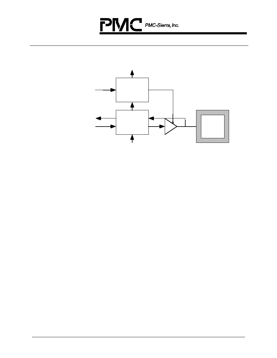
PM6388 EOCTL
DATA SHEET
PMC-1971019
ISSUE 6
OCTAL E1 FRAMER
PROPRIETARY and CONFIDENTIAL to PMC-Sierra Inc. and for its customers' internal use
254
Figure 20
- Layout of Output Enable and Bidirectional Cells
OUTPUT ENABLE
from internal
logic (0 = drive)
INPUT to
internal logic
OUTPUT from
internal logic
Scan Chain In
Scan Chain Out
I/O
PAD
OUT_CELL
IO_CELL

PM6388 EOCTL
DATA SHEET
PMC-1971019
ISSUE 6
OCTAL E1 FRAMER
PROPRIETARY and CONFIDENTIAL to PMC-Sierra Inc. and for its customers' internal use
255
11 OPERATION
11.1 Configuring the EOCTL from Reset
After a system reset (either via the RSTB pin or via the RESET register bit), the
EOCTL will default to the following settings:
Default Settings
Setting
Receiver Section
Transmitter Section
Framing Format
∑ Basic G.704 with CRC
multiframe enabled.
∑ Channel Associated
Signaling is enabled.
∑ Basic G.704 with CRC
multiframe enabled.
∑ Channel Associated
Signaling is enabled.
E1 line interface
∑ RLD[x] inputs NRZ data
sampled on rising
RLCLK[x] edge.
∑ RJAT Clock Divisors (N1,
N2) set to `2F' and the
phase delay of the PLL is
syncronized to RLCLK[x].
∑ TLD[x] outputs NRZ data
updated on falling
TLCLK[x] edge
∑ TJAT Clock Divisors (N1,
N2) set to `2F' and the
phase delay of the PLL is
syncronized to the Egress
backplane clock.
Ingress/Egress
Interfaces
∑ Clock Slave: External
Signaling Mode
∑ Multiplexed ingress
backplane mode disabled
∑ ID[x], ISIG[x] updated on
rising CICLK edge
∑ Elastic Store enabled,
CIFP indicates frame
alignment
∑ ID[x], ISIG[x], IFP[x] held in
high-impedance state
∑ Backplane rate set to
1.544 Mbits G.802 DS1
from E1 mapping
∑ Clock Slave: External
Signaling Mode
∑ Multiplexed egress
backplane mode disabled
∑ ED[x] and ESIG[x]
sampled on rising CECLK
edge
∑ CEFP indicates frame
alignment
∑ Backplane rate set to
1.544 Mbits G.802 DS1
from E1 mapping
Data Link
∑ internal RDLCs disabled
∑ TS16 extracted to RDLC#1
∑ internal TDPRs disabled
(all 1's passed through)
Options
∑ Automatic trunk
conditioning disabled
∑ PRGD configured to
monitor test patterns
∑ PRGD configured to insert
test patterns in the Egress
direction and test for
patterns in the Ingress
direction.

PM6388 EOCTL
DATA SHEET
PMC-1971019
ISSUE 6
OCTAL E1 FRAMER
PROPRIETARY and CONFIDENTIAL to PMC-Sierra Inc. and for its customers' internal use
256
Timing Options
Not applicable
∑ Digital jitter attenuation
enabled, with TLCLK[x]
referenced to CECLK
Diagnostics
∑ All diagnostic modes
disabled
∑ All diagnostic modes
disabled
After reset, the EOCTL needs to be configured for operation in one of the modes
outlined in the Backplane Receive Interface and Backplane Transmit Interface
sections. The following tables illustrate example setups for the various modes. For
more detailed information on setting up the EOCTL, consult the Operations section
of this document.

PM6388 EOCTL
DATA SHEET
PMC-1971019
ISSUE 6
OCTAL E1 FRAMER
PROPRIETARY and CONFIDENTIAL to PMC-Sierra Inc. and for its customers' internal use
257
Ingress Non-Multiplexed Clock Master: Full E1/NxTS
Ingress Direction
Setting
Register
Data
Ingress Line Interface
Set divisors to FFH
X21H, XA1H
X22H, XA2H
`b11111111
`b11111111
Set SYNC = 0
X23H, XA3H `b00100000
Ingress Backplane Interface
Select (A) or (B)
(A) Full E1
Set:
Clock Master Mode
FE and DE (ex. FE = 1, DE = 0)
Select Full E1
X10H, X90H
`b00001001
(B) NxTS
Configure the RPSC
Enable the RPSC
X5CH,XDCH `b00000011
For each channel placed on
ID[x], set the appropriate
channels' NxTS_IDLE bit.
(ex. TS1-16 on ID[x])
RPSC Offset
20H-2FH
30H-3FH
40H-7FH
`b01000000
`b00000000
`b00000000
Set:
Clock Master Mode
FE and DE (ex. FE = 1, DE = 0)
Select NxTS (ex. without F-bit)
X10H, X90H
`b10001001
Turn off high impedance
X12H, X92H
`b00000001

PM6388 EOCTL
DATA SHEET
PMC-1971019
ISSUE 6
OCTAL E1 FRAMER
PROPRIETARY and CONFIDENTIAL to PMC-Sierra Inc. and for its customers' internal use
258
Ingress Non-Multiplexed Clock Slave: ICLK Reference/External Signaling
Ingress Direction
Setting
Register
Data
Ingress Line Interface
Set divisors to FFH
X21H, XA1H
X22H, XA2H
`b11111111
`b11111111
Set SYNC = 0
X23H, XA3H `b00100000
Ingress Backplane Interface
Select (A) or (B)
(A) ICLK Reference
Set:
ICLK Reference
Select ICLK source (ex. 8kHz ref)
X01H, X81H
`b00000000
(B) External Signaling
Set:
External Signaling
X01H, X81H
`b01000000
Set:
Clock Slave Mode
FE and DE (ex. FE = 1, DE = 0)
X10H, X90X
`b00101001
Turn off high impedance
X12H, X92H
`b00000001

PM6388 EOCTL
DATA SHEET
PMC-1971019
ISSUE 6
OCTAL E1 FRAMER
PROPRIETARY and CONFIDENTIAL to PMC-Sierra Inc. and for its customers' internal use
259
Ingress Multiplexed Bus Operation
Ingress Direction
Setting
Register
Data
Ingress Line Interface
Set divisors to FFH
X21H, XA1H
X22H, XA2H
`b11111111
`b11111111
Set SYNC = 0
X23H, XA3H `b00100000
Ingress Backplane Interface
Set:
Clock Slave Mode, 8.192MHz
FE and DE (ex. FE = 1, DE = 0)
X10H, X90H
`b00101011
Set Frame Pulse Type
(ex.
Octant 1 & 2 -> FP Master
Octant 3-8 -> FP Slave)
011H, 091H
111H, 191H
211H, 291H
311H, 391H
`b00000000
`b00100000
`b00100000
`b00100000
Configure Timeslot Offset
013H, 093H
113H, 193H
213H, 293H
313H, 393H
`b00000000
`b00000001
`b00000010
`b00000011
Set:
Enable Multiplexed bus
Select the desired bus
(ex. 1,3,5,7 -> MID[1],
2,4,6,8 -> MID[2])
001H, 101H
201H, 301H
081H, 181H
281H, 381H
`b01001000
`b01001000
`b01011000
`b01011000
Turn off high impedance
X12H, X92H
`b00000001

PM6388 EOCTL
DATA SHEET
PMC-1971019
ISSUE 6
OCTAL E1 FRAMER
PROPRIETARY and CONFIDENTIAL to PMC-Sierra Inc. and for its customers' internal use
260
Egress Non-Multiplexed Clock Master: Full E1/NxTS
Egress Direction
Setting
Register
Data
Egress Line Interface
Set divisors to FFH
X25H, XA5H
X26H, XA6H
`b11111111
`b11111111
Set SYNC = 0
X27H, XA7H `b00100000
Egress Backplane Interface
Select (A) or (B)
(A) Full E1
Set:
Clock Master Mode
FE and DE (ex. FE = 1, DE = 1)
Select Full E1
X18H, X98H
`b00111001
(B) NxTS
Configure the TPSC
Enable the TPSC
X60H,XE0H
`b00000011
For each channel placed on
ED[x], set the appropriate
channels' NxTS_IDLE bit.
(ex. TS1-16 on ED[x])
TPSC Offset
20H-2FH
30H-3FH
40H-7FH
`b01000000
`b00000000
`b00000000
Set:
Clock Master Mode
FE and DE (ex. FE = 1, DE = 1)
Select NxTS
X18H, X98H
`b10011001

PM6388 EOCTL
DATA SHEET
PMC-1971019
ISSUE 6
OCTAL E1 FRAMER
PROPRIETARY and CONFIDENTIAL to PMC-Sierra Inc. and for its customers' internal use
261
Egress Non-Multiplexed Clock Slave: EFP/External Signaling
Egress Direction
Setting
Register
Data
Egress Line Interface
Set divisors to FFH
X25H, XA5H
X26H, XA6H
`b11111111
`b11111111
Set SYNC = 0
X27H, XA7H `b00100000
Egress Backplane Interface
Select (A) or (B)
(A) EFP
Set:
EFP Select
X03H, X83H
`b00000000
(B) External Signaling
Set:
External Signaling
X03H, X83H
`b01000000
Set:
Clock Slave Mode
FE and DE (ex. FE = 1, DE = 1)
X18H, X98X
`b00111001

PM6388 EOCTL
DATA SHEET
PMC-1971019
ISSUE 6
OCTAL E1 FRAMER
PROPRIETARY and CONFIDENTIAL to PMC-Sierra Inc. and for its customers' internal use
262
Egress Multiplexed Bus Operation
Egress Direction
Setting
Register
Data
Egress Line Interface
Set divisors to FFH
X25H, XA5H
X26H, XA6H
`b11111111
`b11111111
Set SYNC = 0
X27H, XA7H `b00100000
Egress Backplane Interface
Set:
Clock Slave Mode, 8.192MHz
FE and DE (ex. FE = 1, DE = 1)
X18H, X98H
`b00111011
Configure Timeslot Offset
013H, 093H
113H, 193H
213H, 293H
313H, 393H
`b00000000
`b00000001
`b00000010
`b00000011
Set:
Enable Multiplexed bus
Select the desired bus
(ex. 1,3,5,7 -> MED[1],
2,4,6,8 -> MED[2])
003H, 103H
203H, 303H
083H, 183H
283H, 383H
`b01000000
`b01000000
`b01010000
`b01010000

PM6388 EOCTL
DATA SHEET
PMC-1971019
ISSUE 6
OCTAL E1 FRAMER
PROPRIETARY and CONFIDENTIAL to PMC-Sierra Inc. and for its customers' internal use
263
In the following tables the "Addr Offset" is the address relative to 000H, 080H, 100H,
180H, 200H, 280H, 300H, or 380H depending on which framer is being configured.
To access the Performance Monitor Registers, the following polling sequence
should be used:
PMON Polling Sequence
Action
Addr
Offset
Data
Effect
Write PMON FER Count Register
(To transfer the PMON registers for
all eight framers, write the
Revision/Chip ID/Global PMON
Update register.)
069H
00H
Latch performance data into PMON
registers
Read FER Count Register
069H
Read Framing bit error event count
Read FEBE Count (LSB) Register
06AH
Read least significant byte of FEBE
event count
Read FEBE Count (MSB) Register
06BH
Read most significant byte of FEBE
event count
Read CRC Count (LSB) Register
06CH
Read most significant byte of CRC
error event count
Read CRC Count (MSB) Register
06DH
Read most significant byte of CRC
error event count
11.2 Using the Multiplexed Backplane
The EOCTL backplane interface can be configured to operate on a Mitel ST
Æ
, AT&T
CHI
Æ
and MVIP PCM 8.192 Mbit/s multiplexed bus. The ingress and egress
backplanes can be configured independently.
11.2.1
Ingress Multiplexed Bus Configuration
To configure the ingress backplane for the multiplexed bus mode, the RATE[1:0] bits
in the BRIF Configuration Register (010H, 090H, 110H, 190H, 210H, 290H, 310H,
390H) must be programmed to the binary value 11 and the ICLKSLV bit must be set
to logic 1. The ISIG_EN bit in the Ingress Interface Options Register (001H, 081H,
101H, 181H, 201H, 281H, 301H, 381H) should be set to logic 1. This sets the
EOCTL ingress interface to work in clock-slave, signaling enabled, multiplexed bus
mode. All eight octants of the EOCTL must have these bits programmed as
specified above.
Next, each octant's data must be configured to be applied to the desired
timeslot/bitslot on the desired bus. There are two 8.192 Mbit/s ingress multiplexed

PM6388 EOCTL
DATA SHEET
PMC-1971019
ISSUE 6
OCTAL E1 FRAMER
PROPRIETARY and CONFIDENTIAL to PMC-Sierra Inc. and for its customers' internal use
264
buses on the EOCTL. Both are required if the full E1 bandwidth is to be output.
The MIBUS2 bit in the Ingress Interface Options Register configures the octant to be
on the second bus (MCICLK[2], MCIFP[2], MID[2], MISIG[2]) if it is logic 1. If
MIBUS2 is set to logic 0, the octant will reside on the first multiplexed bus
(MCICLK[1], MCIFP[1], MID[1], and MISIG[1]). The octant's data is configured for
the desired timeslot by setting the TSOFF[6:0] bits in the BRIF Time Slot Offset
Register and for the desired bitslot by setting the BOFF[2:0] bits in the BRIF Bit
Offset Register.
For example, if it is desired that the first octant's data be output on the first timeslot
(byte) of the multiplexed bus, TSOFF[6:0] should be set to 0. If it is desired to be on
second timeslot of the bus, TSOFF[6:0] should be set to 1. For the third timeslot,
TSOFF[6:0] should be set to 2. For the fourth timeslot, TSOFF[6:0] should be set to
3. Values larger than 3 will move the first byte of the E1 frame away from the
MCIFP reference. For instance, if the first byte of the E1 frame for the octant is
desired to be output 65 bytes away from MCIFP, then the value 65 should be written
to TSOFF[6:0] for that octant.
Bit offsets work the same way. It is possible to shift the octants' output data on a bit-
by-bit basis relative to MCIFP. Setting BOFF_EN to logic 1 in the BRIF Bit Offset
Register and programming the BOFF[2:0] bits will set the bit-offset. Refer to the
Receive Backplane Bit Offset tables (Table 9 and Table 10) for the appropriate
BOFF[2:0] value for a desired offset.
Finally, to activate the octant's data on the selected multiplexed bus, the MIBUS_EN
bit in the Ingress Interface Options Register must be set to logic 1. If MIBUS_EN is
logic 0, that octant will not drive the MID[x] or MISIG[x] outputs. The MID[x] and
MISIG[x] outputs will be tri-stated during any bits in which no octants are configured
to output data. When programming the TSOFF and BOFF bits, one must be careful
not to overlap data from different octants as unexpected outputs may occur.
The ingress multiplexed clocks may be set to double the bus' data rate. If the CMS
register bit in the BRIF Configuration Register is set to logic 1, then the clock rate on
MCICLK[x] will be expected to be 16.384 MHz.
Most of the timing diagrams in this document show them for the non-multiplexed
mode. These can be adapted to the multiplexed mode by envisioning these
diagrams as the result of a divide-down circuit which divides the multiplexed clock by
4 (or 8 if CMS is set to logic 1) and selects only the data from the appropriate
timeslot (which occurs every fourth timeslot of the multiplexed bus).
11.2.2
Egress Multiplexed Bus Configuration
To configure the egress backplane for the multiplexed bus mode, the RATE[1:0] bits
in the BTIF Configuration Register (018H, 098H, 118H, 198H, 218H, 298H, 318H,

PM6388 EOCTL
DATA SHEET
PMC-1971019
ISSUE 6
OCTAL E1 FRAMER
PROPRIETARY and CONFIDENTIAL to PMC-Sierra Inc. and for its customers' internal use
265
398H) must be programmed to the binary value 11 and the ECLKSLV bit must be
set to logic 1. The ESIG_EN bit in the Egress Interface Options Register (003H,
083H, 103H, 183H, 203H, 283H, 303H, 383H) should be set to logic 1. This sets
the EOCTL egress interface to work in clock-slave, signaling enabled, multiplexed
bus mode. All eight octants of the EOCTL must have these bits programmed as
specified above.
Next, each octant's data must be configured to be taken from the appropriate
timeslot/bitslot on the desired bus. There are two 8.192 Mbit/s egress multiplexed
buses on the EOCTL. Both are required if the full E1 bandwidth for all 8 octants is
to be input. The MEBUS2 bit in the Egress Interface Options Register configures
the octant to use the second multiplexed bus (MCECLK[2], MCEFP[2], MED[2],
MESIG[2]) if it is logic 1. If MEBUS2 is set to logic 0, the octant will extract data
from the first multiplexed bus (MCECLK[1], MCEFP[1], MED[1], and MESIG[1]).
The octant's data is configured for the desired timeslot by setting the TSOFF[6:0]
bits in the BTIF Time Slot Offset Register and for the desired bitslot by setting the
BOFF[2:0] bits in the BTIF Bit Offset Register.
For example, if it is desired that the first octant's data be taken from the first timeslot
(byte) of the multiplexed bus, TSOFF[6:0] should be set to 0. If it is desired to be
from the second timeslot of the bus, TSOFF[6:0] should be set to 1. For the third
timeslot, TSOFF[6:0] should be set to 2. For the fourth timeslot, TSOFF[6:0] should
be set to 3. Values larger than 3 will move the first byte of the E1 frame away from
the MCEFP reference. For instance, if the first byte of the E1 frame for the octant is
desired to be output 32 bytes away from MCEFP, then the value 32 should be
written to TSOFF[6:0] for that octant.
Bit offsets work the same way. It is possible to shift the octants' output data on a bit-
by-bit basis relative to MCEFP. Setting BOFF_EN to logic 1 in the BTIF Bit Offset
Register and programming the BOFF[2:0] bits will set the bit-offset. Refer to the
Transmit Backplane Bit Offset tables (Table 13 and Table 14) for the appropriate
BOFF[2:0] value for a desired offset.
If the CMS bit of the BTIF Configuration Register is set to logic 1, then the clock-
speed on MECLK[x] is expected to be 16.384 MHz. All octants on the same
multiplexed bus should have their CMS bit set to the same value to avoid
unexpected results.
Most of the timing diagrams in this document show them for the non-multiplexed
mode. These can be adapted to the multiplexed mode by envisioning these
diagrams as the result of a divide-down circuit which divides the multiplexed clock by
4 (or 8 if CMS is set to logic 1) and selects only the data from the appropriate
timeslot (which occurs every fourth timeslot of the multiplexed bus).

PM6388 EOCTL
DATA SHEET
PMC-1971019
ISSUE 6
OCTAL E1 FRAMER
PROPRIETARY and CONFIDENTIAL to PMC-Sierra Inc. and for its customers' internal use
266
11.3 Using the Per-Timeslot Transmit Data Link Director
The TXCI is used to direct data link insertion from one of the 3 TDPR blocks into
any timeslot. It is capable of controlling insertion of 3 different data links into 3
different timeslots on an E1 link. It is also capable of controlling insertion of data
links into any or all of the bits on the selected timeslot. Finally, it can control
insertion of the data link onto the selected timeslots/bits on all frames, only odd
frames, or only even frames of the E1 CRC multiframe.
By default (DL1_EVEN = 0, DL1_ODD = 0, TS16_EN = 0), data link insertion is
disabled. When TS_16_EN = 1, TDPR #1 is used to source a datalink into timeslot
16 in place of signaling data.
If a data link is desired to be placed on another timeslot using TDPR#X, then
DLX_EVEN and/or DLX_ODD must be set to logic 1. If only DLX_EVEN is set, then
the data link will only be inserted on the selected timeslot/bits on the FAS frames. If
only DLX_ODD is set, then the data link will only be inserted on the selected
timeslot/bits on the NFAS frames.
For example, to insert a data link stream from TDPR#2 onto all bits of timeslot 31 of
all frames, the following TXCI register bits should be set before enabling TDPR#2
(see the section "Using the Internal FDL Transmitter").
1. DL2_EVEN = 1
2. DL2_ODD = 1
3. DL2_TS[4:0] = `b11111
4. DL2_BIT[7:0] = `b11111111
To insert a data link stream from TDPR#1 onto the Sa5 National Bit, the following
TXCI register bits should be set before enabling TDPR#1.
1. DL1_EVEN = 0
2. DL1_ODD = 1
3. TS16_EN = 0
4. DL1_TS[4:0] = `b00000
5. DL1_BIT[7:0] = `b00001000
To disable data link insertion, the DLX_EVEN bit should be set to logic 1 and all
DLX_BIT[7:0] should be set to logic 0.

PM6388 EOCTL
DATA SHEET
PMC-1971019
ISSUE 6
OCTAL E1 FRAMER
PROPRIETARY and CONFIDENTIAL to PMC-Sierra Inc. and for its customers' internal use
267
11.4 Using the Internal FDL Transmitter
The access rate to the TDPR registers is limited by the rate of the high-speed
system clock (XCLK). The TDPR registers should be accessed (with respect to
WRB rising edge and RDB falling edge) at a rate no faster than 1/8 that of the
49.152 MHz XCLK. This time is used by the high-speed system clock to sample the
event, write the FIFO, and update the FIFO status.
Upon reset of the EOCTL, the TDPR should be disabled by setting the EN bit in the
TDPR Configuration Register to logic 0 (default value). An HDLC all-ones Idle signal
will be sent while in this state. The TDPR should then be enabled by setting EN to
logic 1. The FIFOCLR bit should be set and then cleared to initialize the TDPR
FIFO. The TDPR is now ready to transmit.
To initialize the TDPR, the TDPR Configuration Register must be properly set. If
FCS generation is desired, the CRC bit should be set to logic 1. If the block is to be
used in interrupt driven mode, then interrupts should be enabled by setting the
FULLE, OVRE, UDRE, and LFILLE bits in the TDPR Interrupt Enable register to
logic 1. The TDPR operating parameters in the TDPR Upper Transmit Threshold
and TDPR Lower Interrupt Threshold registers should be set to the desired values.
The TDPR Upper Transmit Threshold sets the value at which the TDPR
automatically begins the transmission of HDLC packets, even if no complete
packets are in the FIFO. Transmission will continue until the current packet is
transmitted and the number of bytes in the TDPR FIFO falls to, or below, this
threshold level. The TDPR will always transmit all complete HDLC packets (packets
with EOM attached) in its FIFO. Finally, the TDPR can be enabled by setting the EN
bit to logic 1. If no message is sent after the EN bit is set to logic 1, continuous flags
will be sent.
The TDPR can be used in a polled or interrupt driven mode for the transfer of data.
In the polled mode the processor controlling the TDPR must periodically read the
TDPR Interrupt Status register to determine when to write to the TDPR Transmit
Data register. In the interrupt driven mode, the processor controlling the TDPR uses
the INTB output, the EOCTL Interrupt ID register, and the EOCTL Interrupt Source
registers to identify TDPR interrupts which determine when writes can or must be
done to the TDPR Transmit Data register.
Interrupt Driven Mode:
The TDPR automatically transmits a packet once it is completely written into the
TDPR FIFO. The TDPR also begins transmission of bytes once the FIFO level
exceeds the programmable Upper Transmit Threshold. The CRC bit can be set to
logic 1 so that the FCS is generated and inserted at the end of a packet. The TDPR
Lower Interrupt Threshold should be set to such a value that sufficient warning of an
underrun is given. The FULLE, LFILLE, OVRE, and UDRE bits are all set to logic 1

PM6388 EOCTL
DATA SHEET
PMC-1971019
ISSUE 6
OCTAL E1 FRAMER
PROPRIETARY and CONFIDENTIAL to PMC-Sierra Inc. and for its customers' internal use
268
so an interrupt on INTB is generated upon detection of a FIFO full state, a FIFO
depth below the lower limit threshold, a FIFO overrun, or a FIFO underrun. The
following procedure should be followed to transmit HDLC packets:
1) Wait for data to be transmitted. Once data is available to be transmitted,
then go to step 2.
2) Write the data byte to the TDPR Transmit Data register.
3) If all bytes in the packet have been sent, then set the EOM bit in the TDPR
Configuration register to logic 1. Go to step 1.
4) If there are more bytes in the packet to be sent, then go to step 2.
While performing steps 1 to 4, the processor should monitor for interrupts generated
by the TDPR. When an interrupt is detected, the TDPR Interrupt Routine detailed in
the following text should be followed immediately.
The TDPR will force transmission of the packet information when the FIFO depth
exceeds the threshold programmed with the UTHR[6:0] bits in the TDPR Upper
Transmit Threshold register. Transmission will not stop until the last byte of all
complete packets is transmitted and the FIFO depth is at or below the threshold
limit. The user should watch the FULLI and LFILLI interrupts to prevent overruns
and underruns.
TDPR Interrupt Routine:
Upon assertion of INTB, the source of the interrupt must first be identified by reading
the Interrupt ID register and Interrupt Source registers. Once the source of the
interrupt has been identified as TDPR, then the following procedure should be
carried out:
1) Read the TDPR Interrupt Status register.
2) If UDRI=1, then the FIFO has underrun and the last packet transmitted has
been corrupted and needs to be retransmitted. When the UDRI bit
transitions to logic 1, one Abort sequence and continuous flags will be
transmitted. The TDPR FIFO is held in reset state. To reenable the TDPR
FIFO and to clear the underrun, the TDPR Interrupt Status/UDR Clear
register should be written with any value.
3) If OVRI=1, then the FIFO has overflowed. The packet which the last byte
written into the FIFO belongs to has been corrupted and must be
retransmitted. Other packets in the FIFO are not affected. Either a timer
can be used to determine when sufficient bytes are available in the FIFO or
the user can wait until the LFILLI interrupt is set, indicating that the FIFO

PM6388 EOCTL
DATA SHEET
PMC-1971019
ISSUE 6
OCTAL E1 FRAMER
PROPRIETARY and CONFIDENTIAL to PMC-Sierra Inc. and for its customers' internal use
269
depth is at the lower threshold limit. The next write to the TDPR Transmit
Data register should contain the first byte of the next packet to be
transmitted.
If the FIFO overflows on the packet currently being transmitted (packet is
greater than 128 bytes long), the OVRI bit is set, an Abort signal is
scheduled to be transmitted, the FIFO is emptied, and then flags are
continuously sent until there is data to be transmitted. The FIFO is held in
reset until a write to the TDPR Transmit Data register occurs. This write
contains the first byte of the next packet to be transmitted.
4) If FULLI=1 and FULL=1, then the TDPR FIFO is full and no further bytes
can be written. When in this state, either a timer can be used to determine
when sufficient bytes are available in the FIFO or the user can wait until
the LFILLI interrupt is set, indicating that the FIFO depth is at the lower
threshold limit.
If FULLI=1 and FULL=0, then the TDPR FIFO had reached the FULL state
earlier, but has since emptied out some of its data bytes and now has
space available in its FIFO for more data.
5) If LFILLI=1 and BLFILL=1, then the TDPR FIFO depth is below its lower
threshold limit. If there is more data to transmit, then it should be written to
the TDPR Transmit Data register before an underrun occurs. If there is no
more data to transmit, then an EOM should be set at the end of the last
packet byte. Flags will then be transmitted once the last packet has been
transmitted.
If LFILLI=1 and BLFILL=0, then the TDPR FIFO had fallen below the
lower-threshold state earlier, but has since been refilled to a level above
the lower-threshold level.
Polling Mode:
The TDPR automatically transmits a packet once it is completely written into the
TDPR FIFO. The TDPR also begins transmission of bytes once the FIFO level
exceeds the programmable Upper Transmit Threshold. The CRC bit can be set to
logic 1 so that the FCS is generated and inserted at the end of a packet. The TDPR
Lower Interrupt Threshold should be set to such a value that sufficient warning of an
underrun is given. The FULLE, LFILLE, OVRE, and UDRE bits are all set to logic 0
since packet transmission is set to work with a periodic polling procedure. The
following procedure should be followed to transmit HDLC packets:
1) Wait until data is available to be transmitted, then go to step 2.
2) Read the TDPR Interrupt Status register.

PM6388 EOCTL
DATA SHEET
PMC-1971019
ISSUE 6
OCTAL E1 FRAMER
PROPRIETARY and CONFIDENTIAL to PMC-Sierra Inc. and for its customers' internal use
270
3) If FULL=1, then the TDPR FIFO is full and no further bytes can be written.
Continue polling the TDPR Interrupt Status register until either FULL=0 or
BLFILL=1. Then, go to either step 4 or 5 depending on implementation
preference.
4) If BLFILL=1, then the TDPR FIFO depth is below its lower threshold limit.
Write the data into the TDPR Transmit Data register. Go to step 6.
5) If FULL=0, then the TDPR FIFO has room for at least 1 more byte to be
written. Write the data into the TDPR Transmit Data register. Go to step 6.
6) If more data bytes are to be transmitted in the packet, then go to step 2.
7) If all bytes in the packet have been sent, then set the EOM bit in the TDPR
Configuration register to logic 1. Go to step 1.
11.5 Using the Per-Timeslot Receive Data Link Extractor
The RXCE is used to direct data link extraction from any timeslot. It is capable of
controlling extraction of 3 different data links from 3 different timeslots of an E1 link.
It is also capable of controlling data links extraction from any or all of the bits of the
selected timeslot. Finally, it can control extraction of the data link from the selected
timeslots/bits of all frames, only odd frames, or only even frames of the E1 CRC
multiframe.
By default (DL1_EVEN = 0, DL1_ODD = 0, TS16_EN = 1), extraction of the data link
is to RDLC#1 from TS16 of the E1 link. Note that RDLC#1 must be enabled before
the data link can be properly extracted (see the section "Using the Internal FDL
Receiver").
If a data link is desired to be extracted from another timeslot using RDLC#X, then
DLX_EVEN and/or DLX_ODD must be set to logic 1. If only DLX_EVEN is set, then
the data link will only be extracted from the selected timeslot/bits on the FAS frames.
If only DLX_ODD is set, then the data link will only be extracted from the selected
timeslot/bits on the NFAS frames.
For example, to extract a data link stream to RDLC#3 from all bits of timeslot 15 of
all frames, the following RXCE register bits should be set before enabling RDLC#3.
5. DL3_EVEN = 1
6. DL3_ODD = 1
7. DL3_TS[4:0] = `b01111
8. DL3_BIT[7:0] = `b11111111

PM6388 EOCTL
DATA SHEET
PMC-1971019
ISSUE 6
OCTAL E1 FRAMER
PROPRIETARY and CONFIDENTIAL to PMC-Sierra Inc. and for its customers' internal use
271
To extract a data link stream to RDLC#1 from the Sa5 and Sa7 National Bits, the
following RXCE register bits should be set before enabling RDLC#1.
6. DL1_EVEN = 0
7. DL1_ODD = 1
8. TS16_EN = 0
9. DL1_TS[4:0] = `b00000
10. DL1_BIT[7:0] = `b00001010
11.6 Using the Internal FDL Receiver
The RDLC requires 15 XCLK cycles to process the results of accesses to the RDLC
Status and RDLC Data registers. Thus, accesses to these registers should not
occur at a rate greater than 1/15 of the 49.152 MHz XCLK.
On power up of the system, the RDLC should be disabled by setting the EN bit in
the Configuration Register to logic 0 (default state). The RDLC Interrupt Control
register should then be initialized to enable the INTB output and to select the FIFO
buffer fill level at which an interrupt will be generated. If the INTE bit is not set to
logic 1, the RDLC Status register must be continuously polled to check the interrupt
status (INTR) bit.
After the RDLC Interrupt Control register has been written, the RDLC can be
enabled at any time by setting the EN bit in the RDLC Configuration register to logic
1. When the RDLC is enabled, it will assume the link status is idle (all ones) and
immediately begin searching for flags. When the first flag is found, an interrupt will
be generated, and a dummy byte will be written into the FIFO buffer. This is done to
provide alignment of link up status with the data read from the FIFO. When an abort
character is received, another dummy byte and link down status is written into the
FIFO. This is done to provide alignment of link down status with the data read from
the FIFO. It is up to the controlling processor to check the COLS bit in the RDLC
Status register for a change in the link status. If the COLS bit is set to logic 1, the
FIFO must be emptied to determine the current link status. The first flag and abort
status encoded in the PBS bits is used to set and clear a Link Active software flag.
When the last byte of a properly terminated packet is received, an interrupt is
generated. While the RDLC Status register is being read the PKIN bit will be logic 1.
This can be a signal to the external processor to empty the bytes remaining in the
FIFO or to just increment a number-of-packets-received count and wait for the FIFO
to fill to a programmable level. Once the RDLC Status register is read, the PKIN bit
is cleared to logic 0 . If the RDLC Status register is read immediately after the last
packet byte is read from the FIFO, the PBS[2] bit will be logic 1 and the CRC and
non-integer byte status can be checked by reading the PBS[1:0] bits.

PM6388 EOCTL
DATA SHEET
PMC-1971019
ISSUE 6
OCTAL E1 FRAMER
PROPRIETARY and CONFIDENTIAL to PMC-Sierra Inc. and for its customers' internal use
272
When the FIFO fill level is exceeded, an interrupt is generated. The FIFO must be
emptied to remove this source of interrupt.
The RDLC can be used in a polled or interrupt driven mode for the transfer of frame
data. In the polled mode, the processor controlling the RDLC must periodically read
the RDLC Status register to determine when to read the RDLC Data register. In the
interrupt driven mode, the processor controlling the RDLC must identify the interrupt
source to determine when to read the RDLC Data register.
When the RDLC is identified as the interrupt source, the RDLC should be serviced
as follows:
1) RDLC Status register read. The INTR bit should be logic 1 if the RDLC is
the interrupt source.
2) If OVR = 1, then discard last frame and go to step 1. Overrun causes a
reset of FIFO pointers. Any packets that may have been in the FIFO are
lost.
3) If COLS = 1, then set the EMPTY FIFO software flag.
4) If PKIN = 1, increment the PACKET COUNT. If the FIFO is desired to be
emptied as soon as a complete packet is received, set the EMPTY FIFO
software flag. If the EMPTY FIFO software flag is not set, FIFO emptying
will delayed until the FIFO fill level is exceeded.
5) Read the RDLC Data register.
6) Read the RDLC Status register.
7) If OVR = 1, then discard last frame and go to step 1. Overrun causes a
reset of FIFO pointers. Any packets that may have been in the FIFO are
lost.
8) If COLS = 1, then set the EMPTY FIFO software flag.
9) If PKIN = 1, increment the PACKET COUNT. If the FIFO is desired to be
emptied as soon as a complete packet is received, set the EMPTY FIFO
software flag. If the EMPTY FIFO software flag is not set, FIFO emptying
will delayed until the FIFO fill level is exceeded.
10) Start the processing of FIFO data. Use the PBS[2:0] packet byte status bits
to decide what is to be done with the FIFO data.
10.1) If PBS[2:0] = 001, discard data byte read in step 5 and set the LINK
ACTIVE software flag.

PM6388 EOCTL
DATA SHEET
PMC-1971019
ISSUE 6
OCTAL E1 FRAMER
PROPRIETARY and CONFIDENTIAL to PMC-Sierra Inc. and for its customers' internal use
273
10.2) If PBS[2:0] = 010, discard the data byte read in step 5 and clear the
LINK ACTIVE software flag.
10.3) If PBS[2:0] = 1XX, store the last byte of the packet, decrement the
PACKET COUNT, and check the PBS[1:0] bits for CRC or NVB
errors before deciding whether or not to keep the packet.
10.4) If PBS[2:0] = 000, store the packet data.
11) If FE = 0 and INTR = 1 or FE = 0 and EMPTY FIFO = 1, go to step 5 else
clear the EMPTY FIFO software flag and leave this interrupt service
routine to wait for the next interrupt.
The link state is typically a local software variable. The link state is inactive if the
RDLC is receiving all ones or receiving bit-oriented codes which contain a sequence
of eight ones. The link state is active if the RDLC is receiving flags or data.
If the RDLC data transfer is operating in the polled mode, processor operation is
exactly as shown above for the interrupt driven mode, except that the entry to the
service routine is from a timer, rather than an interrupt.
Figure 21
- Typical Data Frame
8
7
6
5
4
3
2
1
0
1
1
1
1
1
1
0
FLAG
Address (high)
(low)
CONTROL
Frame Check
Sequence
0
1
1
1
1
1
1
0
FLAG
data bytes received
and transferred to
the FIFO Buffer
BIT:
Bit 1 is the first serial bit to be received. When enabled, the primary, secondary and
universal addresses are compared with the high order packet address to determine
a match.

PM6388 EOCTL
DATA SHEET
PMC-1971019
ISSUE 6
OCTAL E1 FRAMER
PROPRIETARY and CONFIDENTIAL to PMC-Sierra Inc. and for its customers' internal use
274
Figure 22
- Example Multi-Packet Operational Sequence
DATA
INT
FE
LA
1
2
3
4 5
6
7
F
F
F
F
A
D
D
D
D
D
D
D
D
D
D D D D D
F
F
F
F
D
D
D
D
F F
F
- flag sequence (01111110)
A
- abort sequence (01111111)
D
- packet data bytes
INT
- active high interrupt output
FE
- internal FIFO empty status
LA
- state of the LINK ACTIVE software flag
Figure 22 shows the timing of interrupts, the state of the FIFO, and the state of the
Data Link relative the input data sequence. The cause of each interrupt and the
processing required at each point is described in the following paragraphs.
At points 1 and 5 the first flag after all ones or abort is detected. A dummy byte is
written in the FIFO, FE goes low, and an interrupt goes high. When the interrupt is
detected by the processor it reads the dummy byte, the FIFO becomes empty, and
the interrupt is removed. The LINK ACTIVE (LA) software flag is set to logic 1.
At points 2 and 6 the last byte of a packet is detected and interrupt goes high.
When the interrupt is detected by the processor, it reads the data and status
registers until the FIFO becomes empty. The interrupt is removed as soon as the
RDLC Status register is read since the FIFO fill level of 8 bytes has not been
exceeded. It is possible to store many packets in the FIFO and empty the FIFO
when the FIFO fill level is exceeded. In either case the processor should use this
interrupt to count the number of packets written into the FIFO. The packet count or
a software time-out can be used as a signal to empty the FIFO.
At point 3 the FIFO fill level of 8 bytes is exceeded and interrupt goes high. When
the interrupt is detected by the processor it must read the data and status registers
until the FIFO becomes empty and the interrupt is removed.

PM6388 EOCTL
DATA SHEET
PMC-1971019
ISSUE 6
OCTAL E1 FRAMER
PROPRIETARY and CONFIDENTIAL to PMC-Sierra Inc. and for its customers' internal use
275
At points 4 or 7 an abort character is detected, a dummy byte is written into the
FIFO, and interrupt goes high. When the interrupt is detected by the processor it
must read the data and status registers until the FIFO becomes empty and the
interrupt is removed. The LINK ACTIVE software flag is cleared.
11.7 Using the PRGD Pattern Generator/Detector
The pattern generator/detector block provides a valuable diagnostic tool, capable of
generating and detecting an enormous variety of pseudo-random and repetitive
patterns. Controlling the PRGD is accomplished by programming four register sets:
the Pattern Generator/Detector Positioning/Control Register (00CH, 08CH, 10CH,
18CH, 20CH, 28CH, 30CH, 38CH), the TPSC Internal Registers 20H-3FH, the SIGX
Internal Registers 40H-5FH, and the PRGD registers.
11.7.1.1
Using PRGD to test E1 link integrity
For example, suppose it is desired to monitor the error rate on a E1 link without
taking the entire E1 offline. A subset of channels should be chosen (say channels
1,3,5 and 7) to carry PRBS instead of data. The TPSC Timeslot Control Bytes for
channels 1,3,5 and 7 must have their TEST bits set to logic 1, and PCCE must be
set in the TPSC Configuration register to enable the per-TS functions. The Pattern
Generator/Detector Positioning/Control Register should be written to its default of
all-zeroes. The PRGD should be configured to generate the desired PRBS
sequence. The selected channels will then be treated as a single, concatenated
data stream in which the selected PRBS will appear. If the device at the far end of
the line can be set to loop back at least the selected channels, then the PRGD can
be used to monitor the return error rate. The RPSC Per-Timeslot Configuration
registers for channels 1,3,5, and 7 must have their TEST bits set to logic 1, and the
PCCE bit set in the RPSC Configuration register to enable the per-TS functions.
The PRGD will then synchronize to the returning pattern, and begin counting errors.
To determine the BER, an periodic accumulation of the PRGD detection registers
may be forced by writing to one of the PRGD Pattern Detector registers, by writing to
the Revision/Chip ID/Global PMON Update register (009H), or via the
AUTOUPDATE feature. The bit error count, bits received count, and previous 32
bits received are then available via the Pattern Detector registers.
In this scenario, any desired combination of channels may be selected. If it is
desired to insert the test pattern in the entire E1, including the framing bits, then
UNF_GEN must be set in the Pattern Generator/Detector Positioning/Control
Register, and framing bit insertion must be disabled by setting FDIS to logic 1 in the
E1 TRAN Configuration Register. To detect such an unframed sequence,
UNF_DET must also be set.

PM6388 EOCTL
DATA SHEET
PMC-1971019
ISSUE 6
OCTAL E1 FRAMER
PROPRIETARY and CONFIDENTIAL to PMC-Sierra Inc. and for its customers' internal use
276
11.7.1.2
Using PRGD to test backplane integrity
If, instead, it is desired to test the backplane side of the system, RXPATGEN may
be set to logic 1 in the Pattern Generator/Detector Positioning/Control Register.
This will cause the pattern to replace the data received in the selected channels of
RLD[x], and will cause the PRGD to search for the desired PRBS on the ED[x]
stream.
11.7.1.3
Generating and detecting repetitive patterns
When a repetitive pattern (such as 1-in-8) is to be generated or detected, the PS bit
must be set to logic 1. The pattern length register must be set to (N-1), where N is
the length of the desired repetitive pattern. Several examples of programming for
common repetitive sequences are given below in the Common Test Patterns
section.
For pattern generation, the desired pattern must be written into the PRGD Pattern
Insertion registers. The repetitive pattern will then be continuously generated. The
generated pattern will be inserted in data stream formed from the selected channels,
but the phase of the pattern cannot be guaranteed.
For pattern detection, the PRGD will determine if a repetitive pattern of the length
specified in the pattern length register exists in the selected channels. It does so by
loading the first N bits from the selected channels, and then monitoring to see if the
pattern loaded repeats itself error free for the subsequent 48 bit periods. It will
repeat this process until it finds a repetitive pattern of length N, at which point it
begins counting errors (and possibly re-synchronizing) in the same way as for
pseudo-random sequences. Note that the PRGD does NOT look for the pattern
loaded into the Pattern Insertion registers, but rather automatically detects any
repetitive pattern of the specified length. The precise pattern detected can be
determined by initiating a PRGD update, setting PDR[1:0] = 00 in the PRGD Control
register, and reading the Pattern Detector registers (which will then contain the 32
bits detected immediately prior to the strobe).
11.7.1.4
Using PRGD with ELST Enabled
If the elastic store is enabled (Ingress interface is in a Clock Slave mode) then the
PRGD will operate on the data output from the ELST. This has two effects: first,
when the framer is out-of-frame, the ELST Idle Code overwrites the received data,
and so patterns cannot be detected in the receive direction until the FRMR finds
frame. If patterns must be detected while the FRMR is out-of-frame, then the UNF
bit must be set in the Receive Line options Register (Reg. 00H in each octant),
disabling the FRMR from finding frame but allowing the data to pass through ELST
untouched. Alternatively, the TRKEN bit in the Ingress Interface Option register can
be set to logic 0 to disable the ELST Idle Code insertion. The second effect is that if
slips occur in the ELST, then the PRGD will be forced to re-synchronize to the
incoming pattern.

PM6388 EOCTL
DATA SHEET
PMC-1971019
ISSUE 6
OCTAL E1 FRAMER
PROPRIETARY and CONFIDENTIAL to PMC-Sierra Inc. and for its customers' internal use
277
Note that the default ELST idle code, which is all-ones, is a repetitive pattern of
every length, so the PRGD will synchronize to it automatically if repetitive patterns
are being detected.
The pattern generator can be configured to generate pseudo random patterns or
repetitive patterns as shown in the Figure 23 below:
Figure 23
- PRGD Pattern Generator
1
2
3
32
LENGTH
PS
TAP
OUTPUT
The pattern generator consists of a 32 bit shift register and a single XOR gate. The
XOR gate output is fed into the first stage of the shift register. The XOR gate inputs
are determined by values written to the length register (PL[4:0]) and the tap register
(PT[4:0]), when the PS bit is low. When PS is high, the pattern detector functions as
a recirculating shift register, with length determined by PL[4:0].
Common Test Patterns
The PRGD can be configured to monitor the standardized pseudo random and
repetitive patterns described in ITU-T O.151. The register configurations required to
generate these patterns and others are indicated in the two tables below:
Table 44
- Pseudo-Random Pattern Generation (PS bit = 0)
Pattern Type
TR
LR
IR#1
IR#2
IR#3
IR#4
TINV
RINV
23 ≠1
00
02
FF
FF
FF
FF
0
0
24 ≠1
00
03
FF
FF
FF
FF
0
0
25-1
01
04
FF
FF
FF
FF
0
0
26 ≠1
04
05
FF
FF
FF
FF
0
0
27 ≠1 (Fractional
T1 LB Activate)
00
06
FF
FF
FF
FF
0
0

PM6388 EOCTL
DATA SHEET
PMC-1971019
ISSUE 6
OCTAL E1 FRAMER
PROPRIETARY and CONFIDENTIAL to PMC-Sierra Inc. and for its customers' internal use
278
Pattern Type
TR
LR
IR#1
IR#2
IR#3
IR#4
TINV
RINV
27 ≠1 (Fractional
T1 LB
Deactivate)
03
06
FF
FF
FF
FF
0
0
27 ≠1
03
06
FF
FF
FF
FF
1
1
29 ≠1 (O.153)
04
08
FF
FF
FF
FF
0
0
210 -1
02
09
FF
FF
FF
FF
0
0
211 -1 (O.152,
O.153)
08
0A
FF
FF
FF
FF
0
0
215 -1 (O.151)
0D
0E
FF
FF
FF
FF
1
1
217 -1
02
10
FF
FF
FF
FF
0
0
218 -1
06
11
FF
FF
FF
FF
0
0
220 -1 (O.153)
02
13
FF
FF
FF
FF
0
0
220 -1 (O.151
QRSS bit=1)
10
13
FF
FF
FF
FF
0
0
221 -1
01
14
FF
FF
FF
FF
0
0
222 -1
00
15
FF
FF
FF
FF
0
0
223 -1 (O.151)
11
16
FF
FF
FF
FF
1
1
225 -1
02
18
FF
FF
FF
FF
0
0
228 -1
02
1B
FF
FF
FF
FF
0
0
229 -1
01
1C
FF
FF
FF
FF
0
0
231 -1
02
1E
FF
FF
FF
FF
0
0
Table 45
- Repetitive Pattern Generation (PS bit = 1)
Pattern Type
TR
LR
IR#1
IR#2
IR#3
IR#4
TINV
RINV
All ones
00
00
FF
FF
FF
FF
0
0
All zeros
00
00
FE
FF
FF
FF
0
0
Alternating
ones/zeros
00
01
FE
FF
FF
FF
0
0

PM6388 EOCTL
DATA SHEET
PMC-1971019
ISSUE 6
OCTAL E1 FRAMER
PROPRIETARY and CONFIDENTIAL to PMC-Sierra Inc. and for its customers' internal use
279
Pattern Type
TR
LR
IR#1
IR#2
IR#3
IR#4
TINV
RINV
Double alternating
ones/zeros
00
03
FC
FF
FF
FF
0
0
3 in 24
00
17
22
00
20
FF
0
0
1 in 16
00
0F
01
00
FF
FF
0
0
1 in 8
00
07
01
FF
FF
FF
0
0
1 in 4
00
03
F1
FF
FF
FF
0
0
DS1 Inband
loopback activate
00
04
F0
FF
FF
0F
0
0
DS1 Inband
loopback deactivate
00
02
FC
FF
FF
FF
0
0
Notes for the Pseudo Random and Repetitive Pattern Generation Tables
1. The PS bit and the QRSS bit are contained in the PRGD Control register
2. TR = Tap Register
3. LR = Shift Register Length Register
4. IR#1 = PRGD Pattern Insertion #1 Register
5. IR#2 = PRGD Pattern Insertion #2 Register
6. IR#3 = PRGD Pattern Insertion #3 Register
7. IR#4 = PRGD Pattern Insertion #4 Register
8. The TINV bit and the RINV bit are contained in the PRGD Control register

PM6388 EOCTL
DATA SHEET
PMC-1971019
ISSUE 6
OCTAL E1 FRAMER
PROPRIETARY and CONFIDENTIAL to PMC-Sierra Inc. and for its customers' internal use
280
11.8 Using the Loopback Modes
The EOCTL provides three loopback modes to aid in network and system
diagnostics. Line loopback can be initiated at any time via the µP interface, but is
usually initiated once an inband loopback activate code is detected. The system
Diagnostic Digital loopback can be initiated at any time by the system via the µP
interface to check the path of system data through the framer. The payload can
also be looped-back on a per-timeslot basis to allow network testing without taking
an entire E1 off-line.
11.8.1 Line
Loopback
When LINE loopback (LINELB) is initiated by writing 10H to the Diagnostics Register
(007H, 087H, 107H, 187H, 207H, 287H, 307H, and 387H), the appropriate E1
framer in the EOCTL is configured to internally connect the jitter-attenuated clock
and data from the RJAT to the transmit line clock and data, TLD[x] and TLCLK[x].
The RJAT may be bypassed if desired. Conceptually, the data flow through a single
T1 framer in this loopback condition is illustrated in Figure 24:
Figure 24
- Line Loopback
FRMR
Framer:
Frame
Alignment,
Alarm
Extraction
ELST
Elastic
Store
BRIF
Ingress
Interface
ID[1:8]
ICLK[1:8]/ISIG[1:8]
IFP[1:8]
RLCLK[1:8]
RLD[1:8]
TJAT
Digital Jitter
Attenuator
TRAN
BasicTransmitter:
Frame Generation,
Alarm Insertion,
Signaling Insertion,
Trunk Conditioning
BTIF
Egress
Interface
TRANSMITTER
TLD[1:8]
TLCLK[1:8]
ED[1:8]
CIFP*
CICLK*
CTCLK*
ECLK[1:8]/EFP[1:8]/ESIG[1:8]
CEFP*
RJAT
Digital Jitter
Attenuator
CECLK*
TOPS
Timing Options
RECEIVER
Line Loopback
11.8.2
Diagnostic Digital Loopback
When Diagnostic Digital loopback (DDLB) is initiated by writing 04H to the Master
Diagnostics Register (009H, 089H, 109H, 189H, 209H, 289H, 309H, and 389H), the

PM6388 EOCTL
DATA SHEET
PMC-1971019
ISSUE 6
OCTAL E1 FRAMER
PROPRIETARY and CONFIDENTIAL to PMC-Sierra Inc. and for its customers' internal use
281
appropriate E1 framer in the EOCTL is configured to internally connect its line clock
and data (TLD[x] and TLCLK[x]) to the receive line clock and data (RLD[x] and
RLCLK[x]) The data flow through a single E1 framer in this loopback condition is
illustrated in Figure 25:
Figure 25
- Diagnostic Digital Loopback
FRMR
Framer:
Frame
Alignment,
Alarm
Extraction
ELST
Elastic
Store
BRIF
Ingress
Interface
ID[1:8]
ICLK[1:8]/ISIG[1:8]
IFP[1:8]
RLCLK[1:8]
RLD[1:8]
TJAT
Digital Jitter
Attenuator
TRAN
BasicTransmitter:
Frame Generation,
Alarm Insertion,
Signaling Insertion,
Trunk Conditioning
BTIF
Egress
Interface
TRANSMITTER
TLD[1:8]
TLCLK[1:8]
ED[1:8]
CIFP*
CICLK*
CTCLK*
ECLK[1:8]/EFP[1:8]/ESIG[1:8]
CEFP*
RJAT
Digital Jitter
Attenuator
CECLK/*
TOPS
Timing Options
RECEIVER
Diagnostic Loopbac k
11.8.3 Per-TS
Loopback
The E1 payload may be looped-back on a per-timeslot (TS) basis through the use of
the TPSC. If all timeslots are looped-back, the result is very similar to Payload
Loopback on the PM6344 EQUAD. In order for per-TS loopback to operate
correctly, the Ingress Interface must be in Clock Master mode, or else CIFP and
CICLK must be connected to CEFP and CECLK, respectively. The LOOP bit must
be set to logic 1 in the TPSC Internal Registers for each TS desired to be looped
back, and the PCCE bit must be set to logic 1 in the TPSC Configuration register.
When all these configurations have been made, the ingress timeslots selected will
overwrite their corresponding egress timeslots; the remaining egress timeslots will
pass through intact. Note that because the egress and ingress streams will not be
multiframe aligned. The data flow in per-TS loopback is illustrated in Figure 26:

PM6388 EOCTL
DATA SHEET
PMC-1971019
ISSUE 6
OCTAL E1 FRAMER
PROPRIETARY and CONFIDENTIAL to PMC-Sierra Inc. and for its customers' internal use
282
Figure 26
- Per-TS Loopback
FRMR
Framer:
Frame
Alignment,
Alarm
Extraction
ELST
Elastic
Store
BRIF
Ingress
Interface
ID[1:8]
ICLK[1:8]/ISIG[1:8]
IFP[1:8]
RLCLK[1:8]
RLD[1:8]
TJAT
Digital Jitter
Attenuator
TRAN
BasicTransmitter:
Frame Generation,
Alarm Insertion,
Signaling Insertion,
Trunk Conditioning
BTIF
Egress
Interface
TRANSMITTER
TLD[1:8]
TLCLK[1:8]
ED[1:8]
CTCLK*
ECLK[1:8]/EFP[1:8]/ESIG[1:8]
CEFP*
RJAT
Digital Jitter
Attenuator
CECLK*
TOPS
Timing Options
RECEIVER
MU X
TPSC
Per-DS0
Serial
Controller
Per-TS Loopback

PM6388 EOCTL
DATA SHEET
PMC-1971019
ISSUE 6
OCTAL E1 FRAMER
PROPRIETARY and CONFIDENTIAL to PMC-Sierra Inc. and for its customers' internal use
283
11.9 Using the Per-TS Serial Controllers
11.9.1 Initialization
Before the TPSC (RPSC) block can be used, a proper initialization of the internal
registers must be performed to eliminate erroneous control data from being
produced on the block outputs. The output control streams should be disabled by
setting the PCCE bit in the TPSC (RPSC) Configuration Register (registers 060H,
0E0H, 160H, 1E0H, 260H, 2E0H, 360H, 3E0H for TPSC; 05CH, 0DCH, 15CH,
1DCH, 25CH, 2DCH, 35CH, 3DCH for RPSC) to logic 0. Then, all 72 locations of
the TPSC (RPSC) must be filled with valid data. Finally, the output streams can be
enabled by setting the PCCE bit in the TPSC (RPSC) Configuration Register to logic
1.
11.9.2 Direct
Access
Mode
Direct access mode to the TPSC or RPSC is not used in the EOCTL. However,
direct access mode is selected by default whenever the EOCTL is reset. The IND
bit within the TPSC and RPSC Configuration Registers must be set to logic 1 after a
reset is applied.
11.9.3 Indirect
Access
Mode
Indirect access mode is selected by setting the IND bit in the TPSC or RPSC
Configuration Register to logic 1. When using the indirect access mode, the status
of the BUSY indication bit should be polled to determine the status of the
microprocessor access: when the BUSY bit is logic 1, the TPSC or RPSC is
processing an access request; when the BUSY bit is logic 0, the TPSC or RPSC has
completed the request.
The indirect write programming sequence for the TPSC (RPSC) is as follows:
1) Check that the BUSY bit in the TPSC (RPSC) µP Access Status Register is
logic 0.
2) Write the channel data to the TPSC (RPSC) Channel Indirect Data Buffer
register.
3) Write RWB=0 and the channel address to the TPSC (RPSC) Channel Indirect
Address/Control Register.
4) Poll the BUSY bit until it goes to logic 0. The BUSY bit will go to logic 1
immediately after step 3 and remain at logic 1 until the request is complete.

PM6388 EOCTL
DATA SHEET
PMC-1971019
ISSUE 6
OCTAL E1 FRAMER
PROPRIETARY and CONFIDENTIAL to PMC-Sierra Inc. and for its customers' internal use
284
5) If there is more data to be written, go back to step 1.
The indirect read programming sequence for the TPSC (RPSC) is as follows:
1) Check that the BUSY bit in the TPSC (RPSC) µP Access Status Register is
logic 0.
2) Write RWB=1 and the channel address to the TPSC (RPSC) Channel Indirect
Address/Control Register.
3) Poll the BUSY bit, waiting until it goes to a logic 0. The BUSY bit will go to
logic 1 immediately after step 2 and remain at logic 1 until the request is
complete.
4) Read the requested channel data from the TPSC (RPSC) Channel Indirect
Data Buffer register.
5) If there is more data to be read, go back to step 1.
Before the RPSC, PCSC or SIGX are configured, the Ingress and Egress
backplanes should be set for the appropriate clock rates and modes.
11.10 Using the Transmit Digital Jitter Attenuator
In using TJAT, it is important to choose the appropriate divisors for the phase
comparison between the selected reference clock and the generated smooth
TLCLK[x[.
11.10.1 Default Application
Upon reset, the EOCTL default condition provides jitter attenuation with TLCLK[x]
referenced to the common egress clock, CECLK. The TJAT SYNC bit is also logic 1
by default. TJAT is configured to divide its input clock rate, CECLK, and its output
clock rate, TLCLK[x], both by 48, which is the maximum length of the FIFO. These
divided down clock rates are then used by the phase comparator to update the
TJAT DPLL. The phase delay between CECLK and TLCLK[x] is synchronized to the
physical data delay through the FIFO. For example, if the phase delay between
CECLK and TLCLK[x] is 12UI, the FIFO will be forced to lag its output data 12 bits
from its input data.
The default mode works well with the common egress clock running at 2.048MHz.

PM6388 EOCTL
DATA SHEET
PMC-1971019
ISSUE 6
OCTAL E1 FRAMER
PROPRIETARY and CONFIDENTIAL to PMC-Sierra Inc. and for its customers' internal use
285
11.10.2 Data Burst Application
In applications where the transmit backplane line rate is operating at instantaneous
frequencies higher than 2.048 MHz, with external gapping, a few factors must be
considered to adequately filter the resultant TLCLK[x] into a smooth 2.048MHz
clock. The magnitude of the phase shifts in the incoming bursty data are too large
to be properly attenuated by the PLL alone. However, the magnitudes, and the
frequency components of these phase shifts are known, and are most often
multiples of 8 kHz.
The phase shifts of the input clock with respect to the generated TLCLKx] in this
case may be large, but when viewed over a longer period, such as a frame, there is
little net phase shift. Therefore, by choosing the divisors appropriately, the large
phase shifts can be filtered out, leaving a stable reference for the DPLL to lock onto.
In this application, the N1 and N2 divisors should be changed to FFH (i.e. divisors of
256). Consequently, the frequency of the clock inputs to the phase discriminator in
the PLL is 8 kHz. The TJAT SYNC option must be disabled, since the divisor
magnitude of 256 is not an integer multiple of the FIFO length, 48.
The self-centering circuitry of the FIFO should be enabled by setting the CENT
register bit. This sets up the FIFO read pointer to be at least 4 UI away from the
end of the FIFO registers, and then disengages. Should variations in the frequency
of input clock or the output clock cause the read pointer to drift to within one unit
interval of FIFO overflow or underflow, the pointer will be incrementally pushed away
by the LIMIT control without any loss of data.
With SYNC disabled, CENT and LIMIT enabled, the maximum tolerable phase
difference between the bursty input clock and the smooth TLCLK[x] is 40UI. Phase
wander between the two clock signals is compensated for by the LIMIT control.
11.10.3 Elastic Store Application
In multiplex applications where the jitter attenuation is not required, the TJAT FIFO
can be used to provide an elastic store function. For example, in an E12 application,
the data is written into the FIFO at 2.048MHz and the data is read out of the FIFO
with a gapped E2 rate clock applied on CTCLK. In this configuration, the Timing
Options OCLKSEL bit should be programmed to 1, and the CTCLKSEL bit should
be programmed to 1. Also, the TJAT SYNC and LIMIT bits should be disabled and
the CENT bit enabled. This provides the maximum phase difference between the
input clock and the gapped output clock of 40UI. The maximum jitter and wander
between the two clocks is 8UIp-p.

PM6388 EOCTL
DATA SHEET
PMC-1971019
ISSUE 6
OCTAL E1 FRAMER
PROPRIETARY and CONFIDENTIAL to PMC-Sierra Inc. and for its customers' internal use
286
11.10.4 Alternate TLCLK Reference Application
In applications where TLCLK[x] is referenced to an Nx8 kHz clock source applied on
CTCLK, TJAT can be configured by programming the output clock divisor, N2, to
C0H and the input clock divisor, N1, to the value (N-1). The resultant input clocks to
the phase comparator are both 8kHz. The TJAT SYNC and LIMIT bits should be
disabled in this configuration.
11.11 Isolating an Interrupt
When the INTB pin goes low, the following procedure may be used to isolate the
interrupt source.
1) Read the Interrupt ID register (Register 00BH). The bit corresponding to any
framer that has an outstanding interrupt will be logic 1.
2) Read the Interrupt Source Registers (Registers 005H and 006H for each framer)
for the framer that caused the interrupt. For instance, if framer 5 caused the
interrupt, then registers 285H and 286H would be read. The bit corresponding to
any block with an outstanding interrupt will be set to logic 1 in these registers.
3) Read the register(s) containing the interrupt status bits of the interrupting block in
order to determine the event causing the interrupt. A typical block interrupt has two
related bits: an enable bit (EVENTE for instance) and an interrupt status bit
(EVENTI for instance). EVENTI will go to logic 1 when the triggering event occurs,
and goes low when the register containing it is read; the setting of EVENTE has no
effect on the value of EVENTI. However, a chip interrupt will only be caused if
EVENTE is logic 1 and EVENTI is logic 1. Thus, both the interrupt status bit(s) and
their respective enables may need to be read in order to determine which event
caused an interrupt. Specific interrupt setups may differ from this model, however.
11.12 Using the Performance Monitor Counter Values
All PMON event counters are of sufficient length so that the probability of counter
saturation over a one second interval is very small (less than 0.001%). The odds of
any one of the counters saturating during a one second sampling interval go up as
the bit error rate (BER) increases. At some point, the probability of counter
saturation reaches 50%. This point varies, depending upon the framing format and
the type of event being counted. The BER at which the probability of counter
saturation reaches 50% is shown for various counters in Table 46.
Table 46
- PMON Counter Saturation Limits
Counter
BER

PM6388 EOCTL
DATA SHEET
PMC-1971019
ISSUE 6
OCTAL E1 FRAMER
PROPRIETARY and CONFIDENTIAL to PMC-Sierra Inc. and for its customers' internal use
287
FER
4.0 X 10⁻³
CRCE
cannot saturate
FEBE
cannot saturate
Below these 50% points, the relationship between the BER and the counter event
count (averaged over many one second samples) is essentially linear. Above the
50% point, the relationship between BER and the average counter event count is
highly non-linear due to the likelihood of counter saturation. The following figures
show this relationship for various counters and framing formats. These graphs can
be used to determine the BER, given the average event count. In general, if the
BER is above 10
-3
, the average counter event count cannot be used to determine
the BER without considering the statistical effect of occasional counter saturation.
The following graph illustrates the expected BEE Count for a range of Bit Error
Ratios.
Figure 27
- FER Count vs. BER
0
50
100
150
200
250
0
1
2
3
4
5
6
7
8
9
Average Count Over
Many 1 Second Intervals
Bit Error Rate (x 10 )
-3
Framing Bit Error Count Per Second
Since the maximum number of CRC sub-multiframes that can occur in one second
is 1000, the 10-bit FEBE and CRCE counters cannot saturate in one second.
Despite this, there is not a linear relationship between BER and CRC-4 block errors
due to the nature of the CRC-4 calculation. At BERs below 10
-4
, there tends to be
no more than one bit error per sub-multiframe, so the number of CRC-4 errors is
generally equal to the number of bit errors, which is directly related to the BER.
However, at BERs above 10
-4
, each CRC-4 error is often due to more than one bit
error. Thus, the relationship between BER and CRCE count becomes non-linear
above a 10
-4
BER. This must be taken into account when using CRC-4 counts to
determine the BER. Since FEBEs are indications of CRCEs at the far end, and are

PM6388 EOCTL
DATA SHEET
PMC-1971019
ISSUE 6
OCTAL E1 FRAMER
PROPRIETARY and CONFIDENTIAL to PMC-Sierra Inc. and for its customers' internal use
288
accumulated identically to CRCEs, the same explanation holds for the FEBE event
counter.
Figure 28
- CRCE Count vs. BER
0
1000
200
400
600
800
1200
0
4
8
12
16
20
Average Count Over
Many 1 Second Intervals
CRC Error Event Count Per Second
Bit Error Rate (x 10 )
-4

PM6388 EOCTL
DATA SHEET
PMC-1971019
ISSUE 6
OCTAL E1 FRAMER
PROPRIETARY and CONFIDENTIAL to PMC-Sierra Inc. and for its customers' internal use
289
11.13 JTAG Support
The EOCTL supports the IEEE Boundary Scan Specification as described in the
IEEE 1149.1 standards. The Test Access Port (TAP) consists of the five standard
pins, TRSTB, TCK, TMS, TDI and TDO used to control the TAP controller and the
boundary scan registers. The TRSTB input is the active-low reset signal used to
reset the TAP controller. TCK is the test clock used to sample data on input, TDI
and to output data on output, TDO. The TMS input is used to direct the TAP
controller through its states. The basic boundary scan architecture is shown in
Figure 29.
Figure 29
- Boundary Scan Architecture
Boundary Scan
Register
Control
TDI
TDO
Device Identification
Register
Bypass
Register
Instruction
Register
and
Decode
TRSTB
TMS
TCK
Test
Access
Port
Controller
Mux
DFF
Select
Tri-state Enable
The boundary scan architecture consists of a TAP controller, an instruction register
with instruction decode, a bypass register, a device identification register and a
boundary scan register. The TAP controller interprets the TMS input and generates

PM6388 EOCTL
DATA SHEET
PMC-1971019
ISSUE 6
OCTAL E1 FRAMER
PROPRIETARY and CONFIDENTIAL to PMC-Sierra Inc. and for its customers' internal use
290
control signals to load the instruction and data registers. The instruction register
with instruction decode block is used to select the test to be executed and/or the
register to be accessed. The bypass register offers a single-bit delay from primary
input TDI to primary output TDO. The device identification register contains the
device identification code.
The boundary scan register allows testing of board inter-connectivity. The boundary
scan register consists of a shift register place in series with device inputs and
outputs. Using the boundary scan register, all digital inputs can be sampled and
shifted out on primary output TDO. In addition, patterns can be shifted in on primary
input TDI and forced onto all digital outputs.
TAP Controller
The TAP controller is a synchronous finite state machine clocked by the rising edge
of primary input, TCK. All state transitions are controlled using primary TMS. The
finite state machine is shown in
Figure 30
.

PM6388 EOCTL
DATA SHEET
PMC-1971019
ISSUE 6
OCTAL E1 FRAMER
PROPRIETARY and CONFIDENTIAL to PMC-Sierra Inc. and for its customers' internal use
291
Figure 30
- TAP Controller Finite State Machine
Test-Logic-Reset
Run-Test-Idle
Select-DR-Scan
Select-IR-Scan
Capture-DR
Capture-IR
Shift-DR
Shift-IR
Exit1-DR
Exit1-IR
Pause-DR
Pause-IR
Exit2-DR
Exit2-IR
Update-DR
Update-IR
TRSTB=0
0
0
0
0
0
0
1
1
1
1
1
1
1
1
1
0
0
0
0
0
1
1
1
1
1
1
All transitions dependent on input TMS
0
0
0
0
0
1
Test-Logic-Reset
The test logic reset state is used to disable the TAP logic when the device is in
normal mode operation. The state is entered asynchronously by asserting input,
TRSTB. The state is entered synchronously regardless of the current TAP controller
state by forcing input, TMS high for 5 TCK clock cycles. While in this state, the
instruction register is set to the IDCODE instruction.

PM6388 EOCTL
DATA SHEET
PMC-1971019
ISSUE 6
OCTAL E1 FRAMER
PROPRIETARY and CONFIDENTIAL to PMC-Sierra Inc. and for its customers' internal use
292
Run-Test-Idle
The run test/idle state is used to execute tests.
Capture-DR
The capture data register state is used to load parallel data into the test data
registers selected by the current instruction. If the selected register does not allow
parallel loads or no loading is required by the current instruction, the test register
maintains its value. Loading occurs on the rising edge of TCK.
Shift-DR
The shift data register state is used to shift the selected test data registers by one
stage. Shifting is from MSB to LSB and occurs on the rising edge of TCK.
Update-DR
The update data register state is used to load a test register''s parallel output latch.
In general, the output latches are used to control the device. For example, for the
EXTEST instruction, the boundary scan test register's parallel output latches are
used to control the device's outputs. The parallel output latches are updated on the
falling edge of TCK.
Capture-IR
The capture instruction register state is used to load the instruction register with a
fixed instruction. The load occurs on the rising edge of TCK.
Shift-IR
The shift instruction register state is used to shift both the instruction register and
the selected test data registers by one stage. Shifting is from MSB to LSB and
occurs on the rising edge of TCK.
Update-IR
The update instruction register state is used to load a new instruction into the
instruction register. The new instruction must be scanned in using the Shift-IR state.
The load occurs on the falling edge of TCK.
The Pause-DR and Pause-IR states are provided to allow shifting through the test
data and/or instruction registers to be momentarily paused.

PM6388 EOCTL
DATA SHEET
PMC-1971019
ISSUE 6
OCTAL E1 FRAMER
PROPRIETARY and CONFIDENTIAL to PMC-Sierra Inc. and for its customers' internal use
293
Boundary Scan Instructions
The following is an description of the standard instructions. Each instruction selects
an serial test data register path between input TDI and output TDO.
BYPASS
The bypass instruction shifts data from input TDI to output TDO with one TCK clock
period delay. The instruction is used to bypass the device.
EXTEST
The external test instruction allows testing of the interconnection to other devices.
When the current instruction is the EXTEST instruction, the boundary scan register
is placed between TDI and TDO. Primary device inputs can be sampled by loading
the boundary scan register using the Capture-DR state. The sampled values can
then be viewed by shifting the boundary scan register using the Shift-DR state.
Primary device outputs can be controlled by loading patterns shifted in through input
TDI into the boundary scan register using the Update-DR state.
SAMPLE
The sample instruction samples all the device inputs and outputs. For this
instruction, the boundary scan register is placed between TDI and TDO. Primary
device inputs and outputs can be sampled by loading the boundary scan register
using the Capture-DR state. The sampled values can then be viewed by shifting the
boundary scan register using the Shift-DR state.
IDCODE
The identification instruction is used to connect the identification register between
TDI and TDO. The device's identification code can then be shifted out using the
Shift-DR state.
STCTEST
The single transport chain instruction is used to test out the TAP controller and the
boundary scan register during production test. When this instruction is the current
instruction, the boundary scan register is connected between TDI and TDO. During
the Capture-DR state, the device identification code is loaded into the boundary
scan register. The code can then be shifted out TDO using the Shift-DR state.

PM6388 EOCTL
DATA SHEET
PMC-1971019
ISSUE 6
OCTAL E1 FRAMER
PROPRIETARY and CONFIDENTIAL to PMC-Sierra Inc. and for its customers' internal use
294
12 FUNCTIONAL
TIMING
By convention, in the following functional timing diagrams, the first bit transmitted
in each timeslot shall be designated bit 1 and the last shall be designated bit 8.
Figure 31
- Ingress Interface Clock Master : Full E1 Mode
1 2 3 4 5 6 7 8 1 2 3 4 5 6 7 8 1 2 3 4 5 6 7 8
1 2 3 4 5 6 7 8 1 2 3 4 5 6 7 8
Timeslot 31
Parity Bit
(if enabled)
Timeslot 0
Timeslot 1
Timeslot 31
Parity Bit
(if enabled)
Timeslot 0
IFP[x]
ICLK[x]
ID[x]
1
The Receive Backplane Configuration register is programmed to select the Clock
Master Full E1 mode. IFP[x] is set high for one ICLK[x] period every frame. The
ROHM, BRXSMFP, and BRXCMFP bits can be set to make IFP[x] show the
Signaling Multiframe pulse, the CRC Multiframe pulse, a composite Signaling/CRC
Multiframe pulse, or all overhead bits.
Figure 32
- Egress Interface Clock Master : Full E1 Mode
1 2 3 4 5 6 7 8 1 2 3 4 5 6 7 8 1 2 3 4 5 6 7 8
1 2 3 4 5 6 7 8 1 2 3 4 5 6 7 8
Timeslot 31
Parity Bit
(if enabled)
Timeslot 0
Timeslot 1
Timeslot 31
Parity Bit
(if enabled)
Timeslot 0
EFP[x]
TLCLK[x]
ED[x]
1
The Transmit Backplane Configuration register is programmed to select the Clock
Master Full E1 mode. ED[x] is clocked in on the active edge of the TLCLK[x]
output. Frame alignment is indicated to an upstream source by EFP[x], which may
be configured to indicate basic frame or composite signaling/CRC multiframe
alignment via the ESFP register bit in the Egress Interface Options register.
PM6388 EOCTL
DATA SHEET
PMC-1971019
ISSUE 6
OCTAL E1 FRAMER
PROPRIETARY and CONFIDENTIAL to PMC-Sierra Inc. and for its customers' internal use
295
Figure 33
- Ingress Interface Clock Master : NxTS Mode
ID[x]
ICLK[x]
1 2 3 4 5 6 7 8
Don't Care
1 2 3 4 5 6 7 8
IFP[x]
Timeslot 31
Timeslot 1
The Receive Backplane Interface Configuration register is programmed to select
NxTS Mode. The RPSC Per-Timeslot Configuration DTRKC bits are programmed
to extract the desired channels. In this example, timeslots 31 and 1 are extracted.
ICLK[x] is gapped so that it is not active for those channels with the associated
DTRKC bits set. If the DE bit and FE in the Receive Backplane Interface
Configuration register is set, ID[x] and IFP[x], respectively, are updated on the rising
edge of ICLK[x] and the functional timing is described by Figure 33 with ICLK[x]
inverted.
Figure 34
- Egress Interface Clock Master : NxTS Mode
1 2 3 4 5 6 7 8
Don't Care
1 2 3 4 5 6 7 8
ED[x]
ECLK[x]
Timeslot 23
Timeslot 25
The Transmit Backplane Interface Configuration register is programmed to select
NxTS Mode. The TPSC Timeslot Control Byte NxTS_IDLE bits are programmed to
insert the desired channels. In this example, the link is configured to only insert
data onto timeslots 23 and 25. ECLK[x] is gapped so that it is not active for those
channels with the associated NxTS_IDLE bits set. The inactive channels will
contain the IDLE code defined for that channel in the TPSC. When the DE bit in
the Transmit Backplane Interface Configuration register is set, ED[x] is sampled on
the falling edge of ECLK[x] and the functional timing is described by Figure 34 with
ECLK[x] inverted.

PM6388 EOCTL
DATA SHEET
PMC-1971019
ISSUE 6
OCTAL E1 FRAMER
PROPRIETARY and CONFIDENTIAL to PMC-Sierra Inc. and for its customers' internal use
296
Figure 35
- Ingress Interface Clock Slave Modes
A B C D
Timeslot 31
D
Timeslot 0
1 2 3 4 5 6 7 8 1 2 3 4 5 6 7 8 1 2 3 4 5 6 7 8
A B C
1 2 3 4 5 6 7 8
A B C D
1 2 3 4 5 6 7 8
Timeslot 0
Timeslot 1
Timeslot 31
CICLK
ID[x]
ISIG[x]
CIFP
1
The Ingress Interface is programmed for Clock Slave mode by setting Receive
Backplane Interface Configuration ICLKSLV register bit to logic 1. The External
Signaling mode is chosen by setting the ISIG_EN register bit in the Ingress
Interface Options register to logic 1. If ISIG_EN is logic 0, ICLK Reference Mode is
chosen. ID[x] is timed to the active edge of CICLK, and is frame-aligned to CIFP.
CIFP need not be provided every frame. ID[x] and ISIG[x] may be configured to
carry a parity bit during the first bit of each frame. In External Signaling mode,
ISIG[x] is active and is aligned as shown. In ICLK Reference mode, ICLK[x] is
active in place of ISIG[x]. ICLK[x] is either a jitter-attenuated line-rate clock
referenced to RLCLK[x] or an 8 kHz clock generated by dividing the smoothed
RLCLK[x] by 256. Note that jitter-attenuation only occurs if the RJAT is not
bypassed.
Figure 36
- Egress Interface Clock Slave : EFP Enabled Mode
Timeslot 0
Timeslot 1
Timeslot 0
1 2 3 4 5 6 7 8 1 2 3 4 5 6 7 8 1 2 3 4 5 6 7 8
1 2 3 4 5 6 7 8 1 2 3 4 5 6 7 8
Timeslot 31
Parity bit
(if enabled)
Timeslot 31
Parity bit
(if enabled)
CECLK
CEFP
EFP[x]
ED[x]
1
1
The Egress Interface is configured for the Clock Slave EFP Enabled mode by
setting the ECLKSLV register bit in the Transmit Backplane Interface Configuration
register to logic 1 and the ESIG_EN register bit in the Egress Interface Options
register to logic 0. EFP[x] may be chosen to indicate alignment of every frame or
the composite CRC and Signaling multiframe alignment as shown in Figure 36 by
setting the ESFP bit in the Egress Interface Options register. EFP[x] goes high
marking the first bit of the Signaling multiframe and goes low following the first bit of

PM6388 EOCTL
DATA SHEET
PMC-1971019
ISSUE 6
OCTAL E1 FRAMER
PROPRIETARY and CONFIDENTIAL to PMC-Sierra Inc. and for its customers' internal use
297
the CRC multiframe. If parity checking is enabled, a parity bit should be inserted on
ED[x] in the first bit of each frame. Note that for EFP[x] to be properly aligned, the
TSOFF[6:0] and BOFF_EN bits in the Transmit Backplane Bit Offset register must
all be set to 0.
Figure 37
- Egress Interface Clock Slave : External Signaling Mode
Timeslot 0
Timeslot 1
1 2 3 4 5 6 7 8
A B C D
1 2 3 4 5 6 7 8 1 2 3 4 5 6 7 8
1 2 3 4 5 6 7 8
A B C D
1 2 3 4 5 6 7 8
Timeslot 31
Parity bit
(if enabled)
Timeslot 31
Parity bit
(if enabled)
Timeslot 0
CECLK
ESIG[x]
CEFP
A B C D
1
ED[x]
The Egress Interface is configured for the Clock Slave External Signaling mode by
setting the ECLKSLV register bit in the Transmit Backplane Interface Configuration
register to logic 1 and the ESIG_EN register bit in the Egress Interface Options
register to logic 1. ED[x] is sampled on the active edge of CECLK. Frame
alignment is specified by CEFP. ESIG[x] should carry the signaling bits for each
channel in bits 5, 6, 7, and 8. These signaling bits will be inserted into the data
stream by the E1 TRAN block. If parity checking is enabled, a parity bit should be
inserted on ED[x] and ESIG[x] in the first bit of each frame. The parity operates on
all bits in the ED[x] and ESIG[x] streams, including the unused bits on ESIG[x].
Figure 38
- Non-Multiplexed Transmit Backplane at 2.048/4.096 MHz
7
1
3
4
5
6
2
8
8
7
5
6
8
1
2
3
4
C
A
B
D
D
7
5
6
1
2
3
4
C
A
B
D
8
1
Tim e Slot 0
Time Slot 1
ED[x]
ESIG[x]
CEFP
2.048 M Hz CECLK
(CM S = 0)
4.096 M Hz CECLK
(CM S = 1)
Tim e Slot 31
A 2.048 Mbit/s backplane is configured by setting the RATE[1:0] bits of the
Transmit Backplane Configuration register to 01. In Figure 38, ED[x] and CEFP
are configured to be sampled on the rising edge of CECLK by setting the DE and
FE bits of the Transmit Backplane Configuration register to a logic 1 and the
External Signaling mode is selected.

PM6388 EOCTL
DATA SHEET
PMC-1971019
ISSUE 6
OCTAL E1 FRAMER
PROPRIETARY and CONFIDENTIAL to PMC-Sierra Inc. and for its customers' internal use
298
The TSOFF[6:0], BOFF_EN and BOFF[2:0] register bits are all logic zero;
therefore, CEFP is expected to be aligned to the first bit of the frame.
Figure 39
- Multiplexed Transmit Backplane at 8.192 and 16.384 MHz
D
B C
A
D
B C
A
D
B C
A
D
B C
A
TS 01
M CEFP
8.1 92 M Hz MC EC LK
(C MS = 0)
M ED[x]
M ESIG[x]
TS02
TS03
T S04
TS 11
T S12
T S13
T S14
D
B C
A
D
B C
A
D
B C
A
D
B C
A
D
B C
A
0
2
3
1
6
4
5
7
D
C
B
A
MESIG[x]
MCEFP
8.192 MHz MCECLK
(CMS = 0)
MED[x]
16.384 MHz MCEILK
(CMS = 1)
A 8.192 Mbit/s backplane is configured by setting the RATE[1:0] bits of the
Transmit Backplane Configuration register to `b11. In Figure 39, MED[x] and
MCEFP are configured to be sampled on the rising edge of MCECLK by setting
the DE and FE bits of the Transmit Backplane Configuration register to a logic 1.
Any of the 8 E1 links can be configured to take any of the MED[x] and MESIG[x]
timeslots from the bus by configuring the TSOFF[6:0] bits in the Transmit
Backplane Timeslot Offset register. If TSOFF[6:0] is set to `b0000000, the first
of the four interleaved bytes is sampled.
Figure 40
- Transmit Concentration Highway Interface
CECLK
CEFP
ED[x]
bit 1 TS 0
bit 2 TS 0
bit 3 TS 0
bit 4 TS 0
bit 5 TS 0
bit 6 TS 0
bit 7 TS 0
bit 8 TS 0
bit 1 TS 1
1
2
3
4
5
6
7
8
9
10
11
12
bit 8 TS 31
bit 7 TS 31
bit 6 TS 31
CER = 4
FE = 0, DE = 0, CMS = 0, BOFF = 000, TSOFF = 0000000
CHI timing is configured by setting the BOFF_EN bit of the Transmit Backplane
Bit Offset register to a logic 1. In Figure 40, the DE and FE register bits are set
to logic 0 so that ED[x], ESIG[x] and CEFP are sampled on the falling edge of
CECLK. CMS is set to logic 0 so that the clock rate is equal to the data rate.
BOFF[2:0] is set to `b000 so that the receive clock edge (CER) is equal to 4 (as

PM6388 EOCTL
DATA SHEET
PMC-1971019
ISSUE 6
OCTAL E1 FRAMER
PROPRIETARY and CONFIDENTIAL to PMC-Sierra Inc. and for its customers' internal use
299
determined by the table in the Transmit Backplane Bit Offset register description
of BOFF[2:0]) and ED[x] is sampled 4 clock edges after CEFP is sampled.
TSOFF is set to `b0000000 so that there is no time slot offset.
Figure 41
- Serial Telecom Bus (ST-Bus), Example 1
CECLK
CEFP
ED[x]
bit 1 TS 0
bit 2 TS 0
bit 3 TS 0
bit 4 TS 0
bit 5 TS 0
bit 6 TS 0
bit 7 TS 0
bit 8 TS 0
bit 1 TS 1
1
bit 8 TS 31
bit 7 TS 31
bit 6 TS 31
FE = 1, DE = 0, CMS = 0, FPINV = 1, BOFF_EN = 0, BOFF = 000, TSOFF = 0000000
ST-Bus timing is configured by clearing the BOFF_EN bit of the Transmit
Backplane Bit Offset register to a logic 0 and setting Transmit Timeslot Offset
register to `b0000000. In Figure 42, the FE register bit is set to logic 1 so that
CEFP is sampled on the rising edge of CECLK. The DE register bit is set to
logic 0 so that ED[x] is sampled on the falling edge of CECLK. CMS is set to
logic 0 so that the clock rate is equal to the data rate. BOFF_EN is set to logic 0
to disable bit offsets. FPINV is set to logic 1 to invert the frame pulse.
When using several octants on a multiplexed ST-Bus at 8.192 MHz clock and
data rate, each octant's BTIF must be configured with a different TSOFF in the
Transmit Timeslot Offset Register.
Figure 42
- Serial Telecom Bus (ST-Bus), Example 2
CECLK
CEFP
ED[x]
bit 1 TS 0
bit 2 TS 0
bit 3 TS 0
1
2
bit 8 TS 31
bit 7 TS 31
bit 6 TS 31
FE = 0, DE = 0, CMS = 1, FPINV = 1, BOFF_EN = 1, BOFF = 111, TSOFF = 0011111
ST-Bus timing at 2.048 MHz data rate and 4.096 MHz clock rate is configured by
setting the BOFF_EN bit of the Transmit Backplane Bit Offset to a logic 1, the
BOFF bits to `b111 and the TSOFF bits of the Transmit Backplane Timelot Offset
to `b0011111. In Figure 43, the DE and FE register bits are set to logic 0 so that
ED[x], ESIG[x] and CEFP are sampled on the falling edge of CECLK. CMS is set

PM6388 EOCTL
DATA SHEET
PMC-1971019
ISSUE 6
OCTAL E1 FRAMER
PROPRIETARY and CONFIDENTIAL to PMC-Sierra Inc. and for its customers' internal use
300
to logic 1 so that the clock rate is equal to two times the data rate. FPINV is set
to logic 1 to invert the frame pulse.
When using several octants on a multiplexed ST-Bus at 8.192 MHz data and a
16.384 clock rate, each octant's BTIF must be configured with a different TSOFF
in the Transmit Timeslot Offset Register. To configure an octant to start in
timeslot 1 (of the 128 available starting timeslots), TSOFF must be set to
`b1111111. To configure an octant to start in timeslot 2, TSOFF must be set to
`b0000000. This sequence continues for all remaining starting timeslots.
Figure 43
- Non-Multiplexed Receive Backplane at 2.048/4.096 MHz
7
1
3
4
5
6
2
8
8
7
5
6
8
1
2
3
4
C
A
B
D
D
7
5
6
1
2
3
4
C
A
B
D
8
1
Tim e Slot 0
Time Slot 1
ID[x]
ISIG[x]
CIFP
Tim e Slot 31
2.048 MHz CICLK
(CMS = 0)
4.096 MHz CICLK
(CMS = 1)
A 2.048 Mbit/s backplane is configured by setting the RATE[1:0] bits of the
Receive Backplane Configuration register to `b01. In Figure 45, ID[x] and CIFP
are configured to be updated on the falling edge of CICLK by setting the DE and
FE bits of the Receive Backplane Configuration register to logic 0 and the
External Signaling mode is selected. The TSOFF[6:0], BOFF_EN and BOFF[2:0]
register bits are all logic zero; therefore, CIFP is expected to be aligned to the
first bit of the frame.
Figure 44
- Multiplexed Receive Backplane at 8.192 and 16.384 MHz
TS 311
MISIG[x]
D
B C
A
MCIFP
8.192 M H z M C IC LK
(C MS = 0)
MID[x]
TS 01
0
2
3
1
6
4
5
7
D
C
B
A
MISIG[x]
MCIFP
8.192 MHz MCICLK
(CMS = 0)
MID[x]
16.384 MHz MCICLK
(CMS = 1)

PM6388 EOCTL
DATA SHEET
PMC-1971019
ISSUE 6
OCTAL E1 FRAMER
PROPRIETARY and CONFIDENTIAL to PMC-Sierra Inc. and for its customers' internal use
301
An 8.192 Mbit/s multiplexed backplane is configured by setting all the RATE[1:0]
bits of the Receive Backplane Configuration registers to `b11. In Figure 44,
MID[x] and MCIFP are configured to be updated on the falling edge of MCICLK
by setting the DE and FE bits of the Receive Backplane Configuration register to
logic 0. TSOFF[6:0] is set to `b0000000 so that the first of the four interleaved
bytes is sampled. In this example, only one link is enabled to be output on the
bus by setting MIBUS_OUTEN to logic 1 in the Ingress Interface Options
register. The MID[x] and MISIG[x] outputs are tri-stated during the other
timeslots.
Figure 45
- Receive Concentration Highway Interface
CICLK
CIFP
ID[x]
bit 1 TS 0
bit 2 TS 0
bit 3 TS 0
bit 4 TS 0
bit 5 TS 0
bit 6 TS 0
bit 7 TS 0
bit 8 TS 0
1
2
3
4
5
6
7
8
9
10
11
12
bit 8 TS 31
bit 7 TS 31
bit 6 TS 31
CER = 3
bit 1 TS 1
FE = 0, DE = 1, CMS = 0, BOFF = 000, TSOFF = 0000000
CHI timing is configured by setting the BOFF_EN bit of the Receive Backplane
Configuration register to a logic 1. In Figure 45, FE is set to logic 0 so that CIFP
is sampled on the rising edge of CICLK. DE is set to logic 1 so that ID[x] is
updated on the rising edge of CICLK. CMS is set to logic 0 so that the clock rate
is equal to the data rate. BOFF[2:0] is set to `b000 so that the transmit clock
edge (CET) is equal to 3 (as determined by the table in the register description of
BOFF[2:0]) and ID[x] is updated 3 clock edges after CIFP is sampled. TSOFF is
set to `b0000000 so that there is no time slot offset.

PM6388 EOCTL
DATA SHEET
PMC-1971019
ISSUE 6
OCTAL E1 FRAMER
PROPRIETARY and CONFIDENTIAL to PMC-Sierra Inc. and for its customers' internal use
302
13
ABSOLUTE MAXIMUM RATINGS
Absolute maximum ratings are the worst case limits that the device can
withstand without sustaining permanent damage. They are not indicative of
normal operating conditions.
Table 47
- EOCTL Absolute Maximum Ratings
Ambient Temperature under Bias
-55∞C to +125∞C
Storage Temperature
-65∞C to +150∞C
Voltage on VDD with Respect to GND
-0.3V to 4.6V
Voltage on BIAS with respect to GND
VDD - 0.3V to 5.5V
Voltage on Any Pin
-0.3V to BIAS + 0.3V
Static Discharge Voltage
±1000 V
Latchup current on any pin
±100 mA
Maximum DC current on any pin
±20 mA
Maximum Lead Temperature
+230 ∞C
Maximum Junction Temperature
+150 ∞C

PM6388 EOCTL
DATA SHEET
PMC-1971019
ISSUE 6
OCTAL E1 FRAMER
PROPRIETARY and CONFIDENTIAL to PMC-Sierra Inc. and for its customers' internal use
303
14 D .C. CHARACTERISTICS
TA= -40∞ to +85∞C, VDD=3.3V ±10%, VDD
BIAS
5.5V
Table 48
- EOCTL D.C. Characteristics
Symbol
Parameter
Min
Typ
Max
Units
Conditions
PHA,
PHD
Power Supply
2.97
3.3
3.63
Volts
BIAS
5V Tolerant
Bias
VDD
5.0
5.5
Volts
I
BIAS
Current into 5V
Bias
6.0
µA
V
BIAS
= 5.5V
V
IL
Input Low
Voltage
0
0.8
Volts
Guaranteed Input
LOW Voltage
V
IH
Input High
Voltage
2.0
BIAS
Volts
Guaranteed Input
HIGH Voltage
V
OL
Output or
Bidirectional
Low Voltage
0.25
0.4
Volts
V
DD
= min,
I
OL
= -3 mA for high
drive outputs
4
and -2
mA for others
3
V
OH
Output or
Bidirectional
High Voltage
2.4
Volts
V
DD
= min,
I
OL
= 3 mA for high
drive outputs
4
and 2
mA for others
3
V
T+
Reset Input
High Voltage
2.0
Volts
V
T-
Reset Input
Low Voltage
0.8
Volts
V
TH
Reset Input
Hysteresis
Voltage
0.5
Volts
I
ILPU
Input Low
Current
1,3
-100
-60
-10
µA
VIL = GND
I
IL
Input Low
Current
2,3
-10
0
+10
µA
VIL = GND

PM6388 EOCTL
DATA SHEET
PMC-1971019
ISSUE 6
OCTAL E1 FRAMER
PROPRIETARY and CONFIDENTIAL to PMC-Sierra Inc. and for its customers' internal use
304
Symbol
Parameter
Min
Typ
Max
Units
Conditions
I
IH
Input High
Current
2,3
-10
0
+10
µA
VIH = V
BIAS
I
DDOP1
Operating
Current
125
300
mA
V
DD
= 3.63 V,
Outputs Unloaded,
XCLK = 49.152 MHz
Backplane Rate =
2.048 MHz
Typical parameter
value includes setting
of V52DIS bit.
I
DDOP2
Operating
Current
145
300
mA
V
DD
= 3.63 V,
Outputs Unloaded,
XCLK = 49.152 MHz
Backplane Rate =
8.192 MHz
Typical parameter
value includes setting
of V52DIS.
Notes on D.C. Characteristics:
1. Input pin or bidirectional pin with internal pull-up resistors.
2. Input pin or bidirectional pin without internal pull-up resistors
3. Negative currents flow into the device (sinking), positive currents flow out of
the device (sourcing).
4. D[7:0], TLCLK[1:8], ISIG/ICLK[1:8], ESIG/ECLK/EFP[1:8].

PM6388 EOCTL
DATA SHEET
PMC-1971019
ISSUE 6
OCTAL E1 FRAMER
PROPRIETARY and CONFIDENTIAL to PMC-Sierra Inc. and for its customers' internal use
305
15 MICROPROCESSOR INTERFACE TIMING CHARACTERISTICS
TA= -40∞ to +85∞C, VDD=3.3V ±10%
Microprocessor Read Access (Figure 46)
Symbol
Parameter
Min
Max
Units
tS
AR
Address to Valid Read Set-up Time
10
ns
tH
AR
Address to Valid Read Hold Time
5
ns
tS
ALR
Address to Latch Set-up Time
10
ns
tH
ALR
Address to Latch Hold Time
10
ns
tV
L
Valid Latch Pulse Width
20
ns
tS
LR
Latch to Read Set-up
0
ns
tH
LR
Latch to Read Hold
5
ns
tP
RD
Valid Read to Valid Data Propagation Delay
80
ns
tZ
RD
Valid Read Negated to Output Tri-state
20
ns
tZ
INTH
Valid Read Negated to INTB high
50
ns

PM6388 EOCTL
DATA SHEET
PMC-1971019
ISSUE 6
OCTAL E1 FRAMER
PROPRIETARY and CONFIDENTIAL to PMC-Sierra Inc. and for its customers' internal use
306
Figure 46
- Microprocessor Read Access Timing
INTB
tZ
INTH
(CSB+RDB)
Valid Data
D[7:0]
tP
RD
tZ
RD
tS
AR
tH
AR
Valid Address
A[9:0]
ALE
tS
ALR
tV
L
tS
LR
tH
ALR
tH
LR
Notes on Microprocessor Read Timing:
1. Output propagation delay time is the time in nanoseconds from the 1.4 Volt point
of the reference signal to the 1.4 Volt point of the output.
2. Maximum output propagation delays are measured with a 50 pF load on the
Microprocessor Interface data bus, (D[7:0]).
3. A valid read cycle is defined as a logical OR of the CSB and the RDB signals.
4. Microprocessor Interface timing applies to normal mode register accesses only.
5. When a set-up time is specified between an input and a clock, the set-up time is
the time in nanoseconds from the 1.4 Volt point of the input to the 1.4 Volt point
of the clock.

PM6388 EOCTL
DATA SHEET
PMC-1971019
ISSUE 6
OCTAL E1 FRAMER
PROPRIETARY and CONFIDENTIAL to PMC-Sierra Inc. and for its customers' internal use
307
6. When a hold time is specified between an input and a clock, the hold time is the
time in nanoseconds from the 1.4 Volt point of the clock to the 1.4 Volt point of
the input.
7. In non-multiplexed address/data bus architectures ALE can be held high;
parameters tS
ALR
, tH
ALR
, tV
L
, and tS
LR
, tH
LR
are not applicable.
8. Parameter tH
AR
is not applicable when address latching is used.

PM6388 EOCTL
DATA SHEET
PMC-1971019
ISSUE 6
OCTAL E1 FRAMER
PROPRIETARY and CONFIDENTIAL to PMC-Sierra Inc. and for its customers' internal use
308
Microprocessor Write Access (Figure 47)
Symbol
Parameter
Min
Max
Units
tS
AW
Address to Valid Write Set-up Time
10
ns
tS
DW
Data to Valid Write Set-up Time
20
ns
tS
ALW
Address to Latch Set-up Time
10
ns
tH
ALW
Address to Latch Hold Time
10
ns
tV
L
Valid Latch Pulse Width
20
ns
tS
LW
Latch to Write Set-up
0
ns
tH
LW
Latch to Write Hold
5
ns
tH
DW
Data to Valid Write Hold Time
5
ns
tH
AW
Address to Valid Write Hold Time
5
ns
tV
WR
Valid Write Pulse Width
40
ns
Figure 47
- Microprocessor Write Access Timing
tH
DW
Valid Data
D[7:0]
tV
WR
tS
AW
tH
AW
tS
DW
(CSB+WRB)
A[9:0]
Valid Address
ALE
tV
L
tS
ALW
tS
LW
tH
ALW
tH
LW

PM6388 EOCTL
DATA SHEET
PMC-1971019
ISSUE 6
OCTAL E1 FRAMER
PROPRIETARY and CONFIDENTIAL to PMC-Sierra Inc. and for its customers' internal use
309
Notes on Microprocessor Interface Write Timing:
1. A valid write cycle is defined as a logical OR of the CSB and the WRB signals.
2. Microprocessor Interface timing applies to normal mode register accesses only.
3. In non-multiplexed address/data bus architectures, ALE can be held high,
parameters tS
ALW
, tH
ALW
, tV
L
, and tS
LW
, tH
LW
are not applicable.
4. Parameters tH
AW
and tS
AW
are not applicable if address latching is used.
5. Output propagation delay time is the time in nanoseconds from the 1.4 Volt point
of the reference signal to the 1.4 Volt point of the output.
6. When a set-up time is specified between an input and a clock, the set-up time is
the time in nanoseconds from the 1.4 Volt point of the input to the 1.4 Volt point
of the clock.
7. When a hold time is specified between an input and a clock, the hold time is the
time in nanoseconds from the 1.4 Volt point of the clock to the 1.4 Volt point of
the input.

PM6388 EOCTL
DATA SHEET
PMC-1971019
ISSUE 6
OCTAL E1 FRAMER
PROPRIETARY and CONFIDENTIAL to PMC-Sierra Inc. and for its customers' internal use
310
16 EOCTL I/O TIMING CHARACTERISTICS
TA= -40∞ to +85∞C, VDD=3.3V ±10%
XCLK=49.152 MHz Input (Figure 48)
Symbol
Description
Min
Max
Units
tLXCLK XCLK Low Pulse Width
4
8
ns
tHXCLK XCLK High Pulse Width
4
8
ns
tXCLK
XCLK Period (typically 1/49.152 MHz)
5
20
ns
Figure 48
- High Speed Clock Timing
XCLK
t
L
t
H
t
XCLK
XCLK
XCLK

PM6388 EOCTL
DATA SHEET
PMC-1971019
ISSUE 6
OCTAL E1 FRAMER
PROPRIETARY and CONFIDENTIAL to PMC-Sierra Inc. and for its customers' internal use
311
Egress Interface Timing - Clock Slave: EFP Enabled Mode (Figure 49)
Symbol
Description
Min
Max
Units
tCECLK Common Egress Clock Frequency
1,2
2.0
2.1
MHz
(Typically 2.048 MHz ± 50 ppm)
t1CECLK Common Egress High Pulse Width
4
145
ns
t0CECLK Common Egress Low Pulse Width
4
145
ns
tSCECLK CECLK to Input Set-up Time
7,9
20
ns
tHCECLK CECLK to Input Hold Time
8,9
20
ns
tPEFP1
CECLK to EFP[x] Propagation delay
9,10,11
30
ns
Figure 49
- Egress Interface Timing - Clock Slave: EFP Enabled Mode
CECLK
Valid
tS
CECLK
tH
CECLK
CEFP
ED[x]
Valid
tP
EFP1
EFP[x]
t0
CECLK
t1
CECLK

PM6388 EOCTL
DATA SHEET
PMC-1971019
ISSUE 6
OCTAL E1 FRAMER
PROPRIETARY and CONFIDENTIAL to PMC-Sierra Inc. and for its customers' internal use
312
Egress Interface Timing - Clock Slave: External Signaling (Figure 50)
Symbol
Description
Min
Max
Units
tCECLK Common Egress Clock Frequency
1,2
2.0
2.1
MHz
(Typically 2.048 MHz ± 50 ppm)
t1CECLK Common Egress High Pulse Width
4
145
ns
t0CECLK Common Egress Low Pulse Width
4
145
ns
tSCECLK CECLK to Input Set-up Time
7,9
20
ns
tHCECLK CECLK to Input Hold Time
8,9
20
ns
Figure 50
- Egress Interface Timing - Clock Slave: External Signaling Mode
CECLK
Valid
tS
CECLK
tH
CECLK
CEFP
ED[x]
ESIG[x]
t0
CECLK
t1
CECLK

PM6388 EOCTL
DATA SHEET
PMC-1971019
ISSUE 6
OCTAL E1 FRAMER
PROPRIETARY and CONFIDENTIAL to PMC-Sierra Inc. and for its customers' internal use
313
Egress Interface Timing - Clock Master: Full E1 Mode (Figure 51)
Symbol
Description
Min
Max
Units
tSTLCLK TLCLK[x] to ED[x] Set-up Time
7,9
20
ns
tHTLCLK TLCLK[x] to ED[x] Hold Time
8,9
20
ns
tPEFP2
TLCLK[x]to EFP[x] Propagation delay
9,10,11
-20
20
ns
Figure 51 - Egress Interface Timing - Clock Master: Full E1 Mode
Valid
tP
EFP2
EFP[x]
TLCLK[x]
Valid
tS
TLCLK
tH
TLCLK
ED[x]
Egress Interface Input Timing - Clock Master : NxTS Mode (Figure 52)
Symbol
Description
Min
Max
Units
tSECLK
ECLK[x] to ED[x] Set-up Time
7,9
20
ns
tHECLK ECLK[x] to ED[x] Hold Time
8,9
20
ns
Figure 52 - Egress Interface Input Timing - Clock Master : NxTS Mode
ECLK[x]
Valid
tS
ECLK
tH
ECLK
ED[x]

PM6388 EOCTL
DATA SHEET
PMC-1971019
ISSUE 6
OCTAL E1 FRAMER
PROPRIETARY and CONFIDENTIAL to PMC-Sierra Inc. and for its customers' internal use
314
Ingress Interface Timing - Clock Slave Modes (Figure 53)
Symbol
Description
Min
Max
Units
tCICLK
Common Ingress Clock Frequency
1,2
2.0
2.1
MHz
(Typically 2.048 MHz ± 50 ppm)
t1CICLK Common Ingress High Pulse Width
4
145
ns
t0CICLK Common Ingress Low Pulse Width
4
145
ns
tSCICLK CICLK to CIFP Set-up Time
7,9
20
ns
tHCICLK CICLK to CIFP Hold Time
8,9
20
ns
tPCICLK CICLK to Ingress Output Prop. Delay
9,10,11
25
ns
Figure 53 - Ingress Interface Timing - Clock Slave Modes
CICLK
Valid
tS
CICLK
tH
CICLK
CIFP
Valid
tP
CICLK
ID[x]
ISIG[x]
IFP[x]
t0
CICLK
t1
CICLK

PM6388 EOCTL
DATA SHEET
PMC-1971019
ISSUE 6
OCTAL E1 FRAMER
PROPRIETARY and CONFIDENTIAL to PMC-Sierra Inc. and for its customers' internal use
315
Ingress Interface Timing - Clock Master Modes (Figure 54)
Symbol
Description
Min
Max
Units
tPICLK
ICLK[x] to Ingress Output Prop. Delay
9,10,11
-20
25
ns
Figure 54 - Ingress Interface Timing - Clock Master Modes
ICLK[x]
Valid
tP
ICLK
ID[x]
IFP[x]

PM6388 EOCTL
DATA SHEET
PMC-1971019
ISSUE 6
OCTAL E1 FRAMER
PROPRIETARY and CONFIDENTIAL to PMC-Sierra Inc. and for its customers' internal use
316
Transmit Line Interface Timing (Figure 55)
Symbol
Description
Min
Max
Units
tCTCLK CTCLK Frequency (when used for TJAT REF),
2.0
2.1
MHz
typically 2.048 MHz± 50 ppm
2,6
tHCTCLK CTCLK High Duration
4
100
ns
(when used for TJAT REF)
tLCTCLK CTCLK Low Duration
4
100
ns
(when used for TJAT REF)
tPTLCLK TLCLK[x] to TLD[x] Output Prop. Delay
9,10,11
-20
20
ns
Figure 55 - Transmit Line Interface Timing
CTCLK
t
L
t
H
t
CTCLK
CTCLK
CTCLK
TLCLK[x]
Valid
tP
TLCLK
TLD[x]]

PM6388 EOCTL
DATA SHEET
PMC-1971019
ISSUE 6
OCTAL E1 FRAMER
PROPRIETARY and CONFIDENTIAL to PMC-Sierra Inc. and for its customers' internal use
317
Receive Line Interface Timing (Figure 56)
Symbol
Description
Min
Max
Units
tRLCLK
RLCLK[x] Frequency,
2.0
2.1
MHz
typically 2.048 MHz± 50 ppm
2,6
tHIRLCLK
RLCLK[x] High Duration
4
100
ns
tLORLCLK RLCLK[x] Low Duration
4
100
ns
tSRLCLK
RLCLK[x] to RLD[x] Set-up Time
7,9
20
ns
tHRLCLK
RLCLK[x] to RLD[x] Hold Time
8,9
20
ns
Figure 56 - Receive Line Interface Input Timing
RLCLK[x]
t
LO
t
HI
t
RLCLK
RLCLK
RLCLK
RLCLK[x]
Valid
tS
RLCLK
tH
RLCLK
RLD[x]

PM6388 EOCTL
DATA SHEET
PMC-1971019
ISSUE 6
OCTAL E1 FRAMER
PROPRIETARY and CONFIDENTIAL to PMC-Sierra Inc. and for its customers' internal use
318
Multiplex Ingress Interface Interface Timing (Figure 57)
Symbol
Description
Min
Max
Units
tMCICLK
MICLK Frequency,
8.0
8.4
MHz
typically 8.192 MHz
2,6
t1MCICLK MCICLK High Duration
4
40
ns
t0MCICLK MCICLK Low Duration
4
40
ns
tSMCICLK MCIIFP to MCICLK Set-up Time
7,9
5
ns
tHMCICLK MCIFP to MCICLK Hold Time
8,9
5
ns
tPMCICLK MCICLK to MIFP[x], MID[x],
25
ns
and MISIG[x] Propagation Time
9,10,11
Figure 57 - Multiplexed Ingress Interface Timing
t
0MCICLK
t
1MCICLK
t
MCICLK
Valid
tS
M CICLK
tH
M CICLK
MCIFP
Valid
tP
MCICLK
MID[x]
MISIG[x]
MIFP[x]
MCICLK

PM6388 EOCTL
DATA SHEET
PMC-1971019
ISSUE 6
OCTAL E1 FRAMER
PROPRIETARY and CONFIDENTIAL to PMC-Sierra Inc. and for its customers' internal use
319
Multiplex Egress Interface Interface Timing (Figure 58)
Symbol
Description
Min
Max
Units
tMCECLK
MECLK Frequency,
8.0
8.4
MHz
typically 8.192 MHz
2,6
t1MCECLK MCECLK High Duration
4
40
ns
t0MCECLK MCECLK Low Duration
4
40
ns
tSMCECLK MCEFP, MED[x], MESIG[x] to
5
ns
MCECLK Set-up Time
7,9
tHMCECLK MCEFP, MED[x], MESIG[x] to
5
ns
MCECLK Hold Time
8,9
Figure 58 - Multiplexed Egress Interface Timing
t
0MCECLK
t
1MCECLK
t
MCECLK
MCECLK
Valid
tS
MCECLK
tH
MCECLK
MCEFP
MED[x]
MESIG[x]
JTAG Interface Timing (Figure 59)
Symbol
Description
Min
Max
Units
t1TCK
TCK high pulse width
5
100
ns
t0TCK
TCK low pulse width
5
100
ns
tSTMS,
tSTDI
TMS and TDI Set-up time to TCK
1
50
ns

PM6388 EOCTL
DATA SHEET
PMC-1971019
ISSUE 6
OCTAL E1 FRAMER
PROPRIETARY and CONFIDENTIAL to PMC-Sierra Inc. and for its customers' internal use
320
Symbol
Description
Min
Max
Units
THTMS,
THTDI
TMS and TDI Hold time to TCK
2
50
ns
TPTDO
TCK Low to TDO Valid
6,7
2
50
ns
TVTRSTB TRSTB minimum pulse width
5
100
ns
Figure 59
- JTAG Port Interface Timing
tS
TMS
tH
TMS
TMS
TCK
tS
TDI
tH
TDI
TDI
tP
TDO
TDO
TCK
TCK
t0
TCK
t1
TRSTB
tV
TRSTB

PM6388 EOCTL
DATA SHEET
PMC-1971019
ISSUE 6
OCTAL E1 FRAMER
PROPRIETARY and CONFIDENTIAL to PMC-Sierra Inc. and for its customers' internal use
321
Notes on AC Timing:
1. CECLK and CICLK can be gapped and/or jittered clock signals subject to the
minimum high and low times shown. These specifications correspond to
nominal XCLK input frequencies.
2. Guaranteed by design for nominal XCLK input frequency (49.152 MHz ±50
ppm).
3. CTCLK can be a jittered clock signal subject to the minimum high and low
times shown. These specifications correspond to nominal XCLK input
frequency of 49.152 MHz ±50 ppm.
4. High pulse width is measured from the 1.4 Volt points of the rise and fall
ramps. Low pulse width is measured from the 1.4 Volt points of the fall
and rise ramps.
5. XCLK accuracy is ± 100 ppm.
6. CTCLK[x] can be a jittered clock signal subject to the minimum high and
low durations tHCTCLK, tLCTCLK. These durations correspond to
nominal XCLK input frequency.
7. When a set-up time is specified between an input and a clock, the set-up
time is the time in nanoseconds from the 1.4 Volt point of the input to the 1.4
Volt point of the clock.
8. When a hold time is specified between an input and a clock, the hold time is
the time in nanoseconds from the 1.4 Volt point of the clock to the 1.4 Volt
point of the input.
9. Setup, hold, and propagation delay specifications are shown relative to the
default active clock edge, but are equally valid when the opposite edge is
selected as the active edge.
10. Output propagation delay time is the time in nanoseconds from the 1.4 Volt
point of the reference signal to the 1.4 Volt point of the output.
11. Output propagation delays are measured with a 50 pF load on all outputs.

PM6388 EOCTL
DATA SHEET
PMC-1971019
ISSUE 6
OCTAL E1 FRAMER
PROPRIETARY and CONFIDENTIAL to PMC-Sierra Inc. and for its customers' internal use
322
17
ORDERING AND THERMAL INFORMATION
PART NO.
DESCRIPTION
PM6388-RI
128 Plastic Quad Flat Pack (PQFP)
PART NO.
AMBIENT TEMPERATURE
Theta Ja
Theta Jc
PM6388-RI
-40∞C to 85∞C
47 ∞C/W
14 ∞C/W

PM6388 EOCTL
DATA SHEET
PMC-1971019
ISSUE 6
OCTAL E1 FRAMER
PROPRIETARY and CONFIDENTIAL to PMC-Sierra Inc. and for its customers' internal use
323
18 MECHANICAL
INFORMATION
Figure 60 - 128 Pin Copper Leadframe Plastic Quad Flat Pack (R Suffix)
E
1
D
E1
D1
e
128
8-12 DEG
A
8-12 DEG
A2
Pin 1
Designator
Nom.
Min.
Max.
Dim.
A
A1
A2
D
D1
E
E1
L
e
b
ccc
PACKAGE TYPE:
BODY SIZE:
14.10
14.00
13.90
0.73
0.88
1.03
0.10
14 x 20 x 2.7 MM
2.82
3.40
0.25
0.53
2.57
2.70
2.87
22.95
23.20
23.45
19.90
20.00
20.10
16.95
17.20
17.45
0.50
0.17
0.22
0.27
SEE DETAIL A
128 PIN METRIC RECTANGULAR PLASTIC QUAD FLATPACK-MQFP
GAGE PLANE, 0.25 ABOVE SEATING PLANE.
DETAIL A
0-7 DEG
PLANE
SEATING
0.13-0.23
C
L
.25
A
0-10 DEG.
ccc
C
LEAD COPLANARITY
NOTES: 1) ALL DIMENSIONS IN MILLIMETER.
b
STANDOFF
A1
3) FOOT LENGTH "L" IS MEASURED AT
C
WITH TOLERANCES AS INDICATED.
2) DIMENSIONS SHOWN ARE NOMINAL

PM6388 EOCTL
DATA SHEET
PMC-1971019
ISSUE 6
OCTAL E1 FRAMER
PROPRIETARY and CONFIDENTIAL to PMC-Sierra Inc. and for its customers' internal use
324
NOTES

PM6388 EOCTL
DATA SHEET
PMC-1971019
ISSUE 6
OCTAL E1 FRAMER
PROPRIETARY and CONFIDENTIAL to PMC-Sierra Inc. and for its customers' internal use
325
NOTES

PM6388 EOCTL
DATA SHEET
PMC-1971019
ISSUE 6
OCTAL E1 FRAMER
None of the information contained in this document constitutes an express or implied warranty by PMC-Sierra, Inc. as to the sufficiency, fitness or
suitability for a particular purpose of any such information or the fitness, or suitability for a particular purpose, merchantability, performance, compatibility
with other parts or systems, of any of the products of PMC-Sierra, Inc., or any portion thereof, referred to in this document. PMC-Sierra, Inc. expressly
disclaims all representations and warranties of any kind regarding the contents or use of the information, including, but not limited to, express and
implied warranties of accuracy, completeness, merchantability, fitness for a particular use, or non-infringement.
In no event will PMC-Sierra, Inc. be liable for any direct, indirect, special, incidental or consequential damages, including, but not limited to, lost profits,
lost business or lost data resulting from any use of or reliance upon the information, whether or not PMC-Sierra, Inc. has been advised of the possibility
of such damage.
© 2000 PMC-Sierra, Inc.
PMC-1971019 (R6) ref PMC-1971007(R6)
Issue date: February 2000
PROPRIETARY AND CONFIDENTIAL TO PMC-SIERRA INC. AND FOR ITS CUSTOMERS' INTERNAL USE
326
CONTACTING PMC-SIERRA, INC.
PMC-Sierra, Inc.
105-8555 Baxter Place Burnaby, BC
Canada V5A 4V7
Tel:
(604) 415-6000
Fax: (604) 415-6200
Document Information:
document@pmc-sierra.com
Corporate Information:
info@pmc-sierra.com
Application Information:
apps@pmc-sierra.com
Web Site:
http://www.pmc-