 | –≠–ª–µ–∫—Ç—Ä–æ–Ω–Ω—ã–π –∫–æ–º–ø–æ–Ω–µ–Ω—Ç: RM5231 | –°–∫–∞—á–∞—Ç—å:  PDF PDF  ZIP ZIP |

Proprietary and Confidential to PMC-Sierra, Inc and for its Customer's Internal Use
Document ID: PMC-2002165, Issue 1
RM5231TM Microprocessor with 32-Bit System Bus Data Sheet
Released
RM5231
RM5231TM Microprocessor with 32-Bit
System Bus
Data Sheet
Proprietary and Confidential
Issue 1, March 2001

RM5231TM Microprocessor with 32-Bit System Bus Data Sheet
Released
Proprietary and Confidential to PMC-Sierra, Inc and for its Customer's Internal Use
2
Document ID: PMC-2002165, Issue 1
Legal Information
Copyright
© 2001 PMC-Sierra, Inc.
The information is proprietary and confidential to PMC-Sierra, Inc., and for its customers' internal use. In
any event, you cannot reproduce any part of this document, in any form, without the express written
consent of PMC-Sierra, Inc.
PMC-2002165 (R1)
Disclaimer
None of the information contained in this document constitutes an express or implied warranty by PMC-
Sierra, Inc. as to the sufficiency, fitness or suitability for a particular purpose of any such information or the
fitness, or suitability for a particular purpose, merchantability, performance, compatibility with other parts
or systems, of any of the products of PMC-Sierra, Inc., or any portion thereof, referred to in this document.
PMC-Sierra, Inc. expressly disclaims all representations and warranties of any kind regarding the contents
or use of the information, including, but not limited to, express and implied warranties of accuracy,
completeness, merchantability, fitness for a particular use, or non-infringement.
In no event will PMC-Sierra, Inc. be liable for any direct, indirect, special, incidental or consequential
damages, including, but not limited to, lost profits, lost business or lost data resulting from any use of or
reliance upon the information, whether or not PMC-Sierra, Inc. has been advised of the possibility of such
damage.
Trademarks
RM5231 is a trademark of PMC-Sierra, Inc.
Contacting PMC-Sierra
PMC-Sierra, Inc.
105-8555 Baxter Place Burnaby, BC
Canada V5A 4V7
Tel: (604) 415-6000
Fax: (604) 415-6200
Document Information: document@pmc-sierra.com
Corporate Information: info@pmc-sierra.com
Technical Support: apps@pmc-sierra.com
Web Site: http://www.pmc-sierra.com

RM5231TM Microprocessor with 32-Bit System Bus Data Sheet
Released
Proprietary and Confidential to PMC-Sierra, Inc and for its Customer's Internal Use
3
Document ID: PMC-2002165, Issue 1
Revision History
Issue
No.
Issue Date
ECN
Number
Originator
Details of Change
1
March 2001
3287
T. Chapman
Applied PMC-Sierra template to existing
MPD (QED) FrameMaker document.
Revised Section 3.14, 3.19, 3.22, 3.25,
3.26, 3.27, 3.30, 3.32, 5, 6, 9.3, 9.4, and
the Packaging Information diagram.

RM5231TM Microprocessor with 32-Bit System Bus Data Sheet
Released
Proprietary and Confidential to PMC-Sierra, Inc and for its Customer's Internal Use
4
Document ID: PMC-2002165, Issue 1
Document Conventions
The following conventions are used in this datasheet:
∑
All signal, pin, and bus names described in the text, such as ExtRqst*, are in boldface
typeface.
∑
All bit and field names described in the text, such as Interrupt Mask, are in an italic-bold
typeface.
∑
All instruction names, such as
MFHI
, are in san serif typeface.

RM5231TM Microprocessor with 32-Bit System Bus Data Sheet
Released
Proprietary and Confidential to PMC-Sierra, Inc and for its Customer's Internal Use
5
Document ID: PMC-2002165, Issue 1
Table of Contents
Legal Information ...........................................................................................................................2
Revision History .............................................................................................................................3
Document Conventions .................................................................................................................4
Table of Contents ..........................................................................................................................5
List of Figures ................................................................................................................................7
List of Tables .................................................................................................................................8
1
Features ..................................................................................................................................9
2
Block Diagram .......................................................................................................................10
3
Hardware Overview ...............................................................................................................11
3.1
Superscalar Dispatch ...................................................................................................11
3.2
CPU Registers .............................................................................................................11
3.3
Pipeline ........................................................................................................................11
3.4
Integer Unit ..................................................................................................................12
3.5
Register File .................................................................................................................12
3.6
ALU ..............................................................................................................................12
3.7
Integer Multiply/Divide ..................................................................................................12
3.8
Floating-Point Co-Processor ........................................................................................13
3.9
Floating-Point Unit .......................................................................................................13
3.10 Floating-Point General Register File ............................................................................15
3.11 System Control Co-processor (CP0) ............................................................................15
3.12 System Control Co-Processor Registers .....................................................................15
3.13 Virtual to Physical Address Mapping ............................................................................16
3.14 Joint TLB ......................................................................................................................17
3.15 Instruction TLB .............................................................................................................18
3.16 Data TLB ......................................................................................................................18
3.17 Cache Memory .............................................................................................................18
3.18 Instruction Cache .........................................................................................................18
3.19 Data Cache ..................................................................................................................19
3.20 Write Buffer ..................................................................................................................20
3.21 System Interface ..........................................................................................................21
3.22 System Address/Data Bus ...........................................................................................21
3.23 System Command Bus ................................................................................................21
3.24 Handshake Signals ......................................................................................................22
3.25 Non-overlapping System Interface ...............................................................................22
3.26 Enhanced Write Modes ................................................................................................23
3.27 External Requests ........................................................................................................24
3.28 Interrupt Handling ........................................................................................................24
3.29 Standby Mode ..............................................................................................................24
3.30 JTAG Interface .............................................................................................................24

RM5231TM Microprocessor with 32-Bit System Bus Data Sheet
Released
Proprietary and Confidential to PMC-Sierra, Inc and for its Customer's Internal Use
6
Document ID: PMC-2002165, Issue 1
3.31 Boot-Time Options .......................................................................................................24
3.32 Boot-Time Modes .........................................................................................................25
4
Pin Descriptions ....................................................................................................................26
5
Absolute Maximum Ratings ..................................................................................................29
6
Recommended Operating Conditions ...................................................................................30
7
DC Electrical Characteristics .................................................................................................31
8
Power Consumption ..............................................................................................................32
9
AC Electrical Characteristics .................................................................................................33
9.1
Capacitive Load Deration .............................................................................................33
9.2
Clock Parameters ........................................................................................................33
9.3
System Interface Parameters .......................................................................................34
9.4
Boot-Time Interface Parameters ..................................................................................34
10 Timing Diagrams ...................................................................................................................35
10.1 System Interface Timing ..............................................................................................35
11 Packaging Information ..........................................................................................................36
12 RM5231 128-pin PQFP Package Pinout ...............................................................................38
13 Ordering Information .............................................................................................................39

RM5231TM Microprocessor with 32-Bit System Bus Data Sheet
Released
Proprietary and Confidential to PMC-Sierra, Inc and for its Customer's Internal Use
7
Document ID: PMC-2002165, Issue 1
List of Figures
Figure 1 Block Diagram .............................................................................................................10
Figure 2 CPU Registers .............................................................................................................11
Figure 3 Pipeline ........................................................................................................................12
Figure 4 CP0 Registers .............................................................................................................16
Figure 5 Kernel Mode Virtual Addressing ..................................................................................17
Figure 6 Typical Embedded System Block Diagram ................................................................21
Figure 7 Processor Block Read .................................................................................................23
Figure 8 Processor Block Write .................................................................................................23
Figure 9 Clock Timing ................................................................................................................35
Figure 10 Input Timing ...............................................................................................................35
Figure 11 Output Timing ............................................................................................................35

RM5231TM Microprocessor with 32-Bit System Bus Data Sheet
Released
Proprietary and Confidential to PMC-Sierra, Inc and for its Customer's Internal Use
8
Document ID: PMC-2002165, Issue 1
List of Tables
Table 1 Integer Multiply/Divide Operations ................................................................................13
Table 2 Floating-Point Instruction Cycles ..................................................................................14
Table 3 Cache Attributes ...........................................................................................................20
Table 4 Boot-Time Mode Bit Stream .........................................................................................25
Table 5 System Interface ...........................................................................................................26
Table 6 Clock/Control Interface .................................................................................................27
Table 7 Interrupt Interface .........................................................................................................27
Table 8 JTAG Interface .............................................................................................................27
Table 9 Initialization Interface ....................................................................................................28
Table 10 Power Supply .............................................................................................................28

Proprietary and Confidential to PMC-Sierra, Inc and for its Customer's Internal Use
9
Document ID: PMC-2002165, Issue 1
RM5231TM Microprocessor with 32-bit System Bus Data Sheet
Released
1
Features
∑
Dual Issue superscalar microprocessor
∑
150, 200, & 250 MHz operating frequencies
∑
300 Dhrystone2.1 MIPS
∑
System interface optimized for embedded applications
∑
32-bit system interface lowers total system cost
∑
High-performance write protocols maximize uncached write bandwidth
∑
Processor clock multipliers: 2, 2.5, 3, 3.5, 4, 4.5, 5, 6, 7, 8, 9
∑
2.5 V core with 3.3 V IOs
∑
IEEE 1149.1 JTAG boundary scan
∑
Integrated on-chip caches
∑
32 KB instruction and 32 KB data -- 2 way set associative
∑
Per set locking
∑
Virtually indexed, physically tagged
∑
Write-back and write-through on a per page basis
∑
Pipeline restart on first doubleword for data cache misses
∑
Integrated memory management unit
∑
Fully associative joint TLB (shared by I and D translations)
∑
48 dual entries map 96 pages
∑
Variable page size (4 KB to 16 MB in 4x increments)
∑
High-performance floating-point unit -- up to 500 MFLOPS
∑
Single cycle repeat rate for common single-precision operations and some double pre-
cision operations
∑
Two cycle repeat rate for double-precision multiply and double precision combined
multiply-add operations
∑
Single cycle repeat rate for single-precision combined multiply-add operation
∑
MIPS IV instruction set
∑
Floating point multiply-add instruction increases performance in signal processing
and graphics applications
∑
Conditional moves to reduce branch frequency
∑
Index address modes (register + register)
∑
Embedded application enhancements
∑
Specialized DSP integer Multiply-Accumulate instructions and 3-operand multiply
instruction
∑
I and D cache locking by set
∑
Optional dedicated exception vector for interrupts
∑
Fully static 0.25 micron CMOS design with power down logic
∑
Standby reduced power mode with
WAIT
instruction
∑
2.5 V core with 3.3 V I/O
∑
128-pin Power-Quad 4 (QFP) package

Proprietary and Confidential to PMC-Sierra, Inc and for its Customer's Internal Use
10
Document ID: PMC-2002165, Issue 1
RM5231TM Microprocessor with 32-bit System Bus Data Sheet
Released
2
Block Diagram
Figure 1 Block Diagram
Integer Address/Adder
Instruction Dispatch Unit
Primary Data Cache
2-way Set Associative
Primary Instruction Cache
2-way Set Associative
DTag
DTLB
ITag
ITLB
FP
Instruction
Register
Integer
Instruction
Register
Store Buffer
Write Buffer
Read Buffer
Pad Buffer
Address Buffer
Load Aligner
Integer Register File
DTLB Virtual
PLL/Clocks
Floating-Point
Load/Align
Floating-Point
Register File
Packer/Unpacker
Floating-Point
MultAdd, Add, Sub,
Cvt, Div, Sqrt
Joint TLB
Coprocessor 0
System/Memory
Control
PC Incrementer
Branch PC Adder
ITLB Virtual
Program Counter
Int Mult, Div, Madd
Floating-Point Control
Integer Control
DVA
IVA
Pad Bus
D Bus
FP Bus
Integer Bus
FA Bus
A/D Bus
Shifter/Store Aligner
Logic Unit
Proprietary and Confidential to PMC-Sierra, Inc and for its Customer's Internal Use
11
Document ID: PMC-2002165, Issue 1
RM5231TM Microprocessor with 32-bit System Bus Data Sheet
Released
3
Hardware Overview
The RM5231 offers a high-level of integration targeted at high-performance embedded
applications. The key elements of the RM5231 are briefly described in this section.
3.1
Superscalar Dispatch
The RM5231 has an asymmetric superscalar dispatch unit which allows it to issue an integer
instruction and a floating-point computation instruction simultaneously. Integer instructions
include ALU, branch, load/store, and floating-point load/store, while floating-point computation
instructions include floating-point add, subtract, combined multiply-add, converts, etc. In
combination with its high-throughput fully pipelined floating-point execution unit, the superscalar
capability of the RM5231 provides unparalleled price/performance in computationally intensive
embedded applications.
3.2
CPU Registers
The RM5231 CPU has a user-visible state consisting of 32 general purpose registers, two special
purpose registers for integer multiplication and division, a program counter, and no condition code
bits. Figure 2 shows the user visible state.
Figure 2 CPU Registers
3.3
Pipeline
For integer operations, loads, stores, and other non-floating-point operations, the RM5231 uses a
5-stage pipeline. In addition to the integer pipeline, the RM5231 uses an extended 7-stage pipeline
for floating-point operations.
Figure 3 shows the RM5231 integer pipeline. As illustrated in the figure, up to five integer
instructions can be executing simultaneously.
General Purpose Registers
63
0
Multiply/Divide Registers
0
63
0
r1
HI
r2
63
0
∑
LO
∑
∑
Program Counter
∑
63
0
r29
PC
r30
r31
Proprietary and Confidential to PMC-Sierra, Inc and for its Customer's Internal Use
12
Document ID: PMC-2002165, Issue 1
RM5231TM Microprocessor with 32-bit System Bus Data Sheet
Released
Figure 3 Pipeline
3.4
Integer Unit
The RM5231 integer unit includes thirty-two general purpose 64-bit registers, a load/store
architecture with single cycle ALU operations (add, sub, logical, shift) and an autonomous
multiply/divide unit. Additional register resources include: the HI/LO result registers for the two-
operand integer multiply/divide operations, and the program counter (PC).
The RM5231 implements the MIPS IV Instruction Set Architecture, and is therefore fully upward
compatible with applications that run on processors implementing the earlier generation MIPS I-
III instruction sets.
3.5
Register File
The RM5231 has thirty-two general purpose registers with register location 0 (r0) hard wired to a
zero value. These registers are used for scalar integer operations and address calculation. The
register file has two read ports and one write port and is fully bypassed to minimize operation
latency in the pipeline.
3.6
ALU
The RM5231 ALU consists of an integer adder/subtractor, a logic unit, and a shifter. The adder
performs address calculations in addition to arithmetic operations. The logic unit performs all
logical and zero shift data moves. The shifter performs shifts and store alignment operations. Each
of these units is optimized to perform all operations in a single processor cycle.
3.7
Integer Multiply/Divide
The RM5231 has a dedicated integer multiply/divide unit optimized for high-speed multiply and
multiply-accumulate operations. Table 1 shows the performance of the multiply/divide unit on
each operation.
I0
I1
I2
I3
I4
2I
1I
1R
2R
1A
2A
1D
2D
1W
2W
2I
1I
1R
2R
1A
2A
1D
2D
1W
2W
2I
1I
1R
2R
1A
2A
1D
2D
1W
2W
2I
1I
1R
2R
1A
2A
1D
2D
1W
2W
2I
1I
1R
2R
1A
2A
1D
2D
1W
2W
one cycle
1I-1R:
2I:
2A-2D:
2R:
1A-2A:
1A:
1A:
1D:
2A:
2W:
Instruction cache access
Instruction virtual to physical address translation
Register file read, Bypass calculation, Instruction decode, Branch address calculation
Issue or slip decision, Branch decision
Integer add, logical, shift
Data virtual address calculation
Data virtual to physical address translation
Store Align
Register file write
Data cache access and load align

Proprietary and Confidential to PMC-Sierra, Inc and for its Customer's Internal Use
13
Document ID: PMC-2002165, Issue 1
RM5231TM Microprocessor with 32-bit System Bus Data Sheet
Released
Table 1 Integer Multiply/Divide Operations
The baseline MIPS IV ISA specifies that the results of a multiply or divide operation be placed in
the Hi and Lo registers. These values can then be transferred to the general purpose register file
using the Move-from-Hi and Move-from-Lo (
MFHI
/
MFLO
) instructions.
In addition to the baseline MIPS IV integer multiply instructions, the RM5231 also implements the
3 operand multiply instruction,
MUL
. This instruction specifies that the multiply result go directly
to the integer register file rather than the Lo register. The portion of the multiply that would have
normally gone into the Hi register is discarded. For applications where it is known that the upper
half of the multiply result is not required, using the
MUL
instruction eliminates the necessity of
executing an explicit
MFLO
instruction.
Also included in the RM5231 are the multiply-add instructions,
MADU
/
MAD
. This instruction
multiplies two operands and adds the resulting product to the current contents of the Hi and Lo
registers. The multiply-accumulate operation is the core primitive of almost all signal processing
algorithms allowing the RM5231 to eliminate the need for a separate DSP engine in many
embedded applications.
3.8
Floating-Point Co-Processor
The RM5231 incorporates a high-performance fully pipelined floating-point co-processor which
includes a floating-point register file and autonomous execution units for multiply/add/convert and
divide/square root. The floating-point coprocessor is a tightly coupled execution unit, decoding
and executing instructions in parallel with, and in the case of floating-point loads and stores, in
cooperation with the integer unit. The superscalar capabilities of the RM5231 allow floating-point
computation instructions to issue concurrently with integer instructions.
3.9
Floating-Point Unit
The RM5231 floating-point execution unit supports single and double precision arithmetic, as
specified in the IEEE Standard 754. The execution unit is broken into a separate divide/square root
unit and a pipelined multiply/add unit. Overlap of the divide/square root and multiply/add
operations is supported.
The RM5231 maintains fully precise floating-point exceptions while allowing both overlapped
and pipelined operations. Precise exceptions are extremely important in object-oriented
programming environments and highly desirable for debugging in any environment.
Opcode
Operand
Size
Latency
Repeat
Rate
Stall
Cycles
MULT/U,
MAD/U
16 bit
3
2
0
32 bit
4
3
0
MUL
16 bit
3
2
1
32 bit
4
3
2
DMULT,
DMULTU
any
7
6
0
DIV, DIVD
any
36
36
0
DDIV,
DDIVU
any
68
68
0
Proprietary and Confidential to PMC-Sierra, Inc and for its Customer's Internal Use
14
Document ID: PMC-2002165, Issue 1
RM5231TM Microprocessor with 32-bit System Bus Data Sheet
Released
Floating-point operations includes:
∑
add
∑
subtract
∑
multiply
∑
divide
∑
square root
∑
reciprocal
∑
reciprocal square root
∑
conditional moves
∑
conversion between fixed-point and floating-point format
∑
conversion between floating-point formats, and floating-point compare.
Table 2 gives the latencies of the floating-point instructions in internal processor cycles.
Table 2 Floating-Point Instruction Cycles
Operation
Latency
Repeat Rate
fadd
4
1
fsub
4
1
fmult
4/5
1/2
fmadd
4/5
1/2
fmsub
4/5
1/2
fdiv
21/36
19/34
fsqrt
21/36
19/34
frecip
21/36
19/34
frsqrt
38/68
36/66
fcvt.s.d
4
1
fcvt.s.w
6
3
fcvt.s.l
6
3
fcvt.d.s
4
1
fcvt.d.w
4
1
fcvt.d.l
4
1
fcvt.w.s
4
1
fcvt.w.d
4
1
fcvt.l.s
4
1
fcvt.l.d
4
1
fcmp
1
1
fmov
1
1
fmovc
1
1
fabs
1
1
fneg
1
1
Note:
Numbers are represented as single/double precision format.

Proprietary and Confidential to PMC-Sierra, Inc and for its Customer's Internal Use
15
Document ID: PMC-2002165, Issue 1
RM5231TM Microprocessor with 32-bit System Bus Data Sheet
Released
3.10 Floating-Point General Register File
The floating-point general register file (FGR) is made up of thirty-two 64-bit registers. With the
floating-point load and store double instructions (
LDC1
and
SDC1
), the floating-point unit can
take advantage of the 64-bit wide data cache and issue a floating-point co-processor load or store
doubleword instruction in every cycle.
The floating-point control register space contains two registers; one for determining configuration
and revision information for the coprocessor and one for control and status information. These are
primarily used for diagnostic software, exception handling, state saving and restoring, and control
of rounding modes. To support superscalar operation, the FGR has four read ports and two write
ports, and is fully bypassed to minimize operation latency in the pipeline. Three of the read ports
and one write port are used to support the combined multiply-add instruction while the fourth read
and second write port allows a concurrent floating-point load or store.
3.11 System Control Co-processor (CP0)
The system control co-processor, also called coprocessor 0 or CP0 in the MIPS architecture, is
responsible for the virtual memory sub-system, the exception control system, and the diagnostics
capability of the processor. In the MIPS architecture, the system control co-processor (and thus the
kernel software) is implementation dependent.
The memory management unit controls the virtual memory system page mapping. It consists of an
instruction address translation buffer, ITLB, a data address translation buffer, DTLB, a Joint
instruction and data address translation buffer, JTLB, and co-processor registers used by the virtual
memory mapping sub-system.
3.12 System Control Co-Processor Registers
The RM5231 incorporates all system control co-processor (CP0) registers on-chip. These registers
provide the path through which the virtual memory system's page mapping is examined and
modified, exceptions are handled, and operating modes are controlled (kernel vs. user mode,
interrupts enabled or disabled, cache features). In addition, the RM5231 includes registers to
implement a real-time cycle counting facility to aid in cache diagnostic testing and to assist in data
error detection.
Figure 4 shows the CP0 registers.

Proprietary and Confidential to PMC-Sierra, Inc and for its Customer's Internal Use
16
Document ID: PMC-2002165, Issue 1
RM5231TM Microprocessor with 32-bit System Bus Data Sheet
Released
Figure 4 CP0 Registers
3.13 Virtual to Physical Address Mapping
The RM5231 provides three modes of virtual addressing:
∑
user mode
∑
kernel mode
∑
supervisor mode
This mechanism is available to system software to provide a secure environment for user
processes. Bits in the CP0 Status register determine which virtual addressing mode is used. In the
user mode, the RM5231 provides a single, uniform virtual address space of 1TB (2 GB in 32-bit
mode).
When operating in the kernel mode, four distinct virtual address spaces, totalling over 2.5 TB (4
GB in 32-bit mode), are simultaneously available and are differentiated by the high-order bits of
the virtual address.
The RM5231 processors also support a supervisor mode in which the virtual address space over 2
TB (2.5 GB in 32-bit mode), divided into three regions based on the high-order bits of the virtual
address.
When the RM5231 is configured as a 64-bit microprocessor, the virtual address space layout is an
upward compatible extension of the 32-bit virtual address space layout.
Figure 5 shows the address space layout for 32-bit operation.
0
47
TLB
(entries protected
from TLBWR)
EntryHi
10*
EntryLo0
2*
EntryLo1
3*
PageMask
5*
Wired
6*
Random
1*
Index
0*
Status
12*
Cause
13*
EPC
14*
ErrorEPC
30*
Count
9*
Compare
11*
Context
4*
PRId
15*
Config
16*
TagHi
29*
TagLo
28*
ECC
26*
CacheErr
27*
BadVAddr
8*
LLAddr
17*
* Register number
XContext
20*
Used for memory
management
Used for exception
processing

Proprietary and Confidential to PMC-Sierra, Inc and for its Customer's Internal Use
17
Document ID: PMC-2002165, Issue 1
RM5231TM Microprocessor with 32-bit System Bus Data Sheet
Released
Figure 5 Kernel Mode Virtual Addressing (32-bit)
3.14 Joint TLB
For fast virtual-to-physical address translation, the RM5231 uses a large, fully associative TLB
that maps 96 virtual pages to their corresponding physical addresses. As indicated by its name, the
joint TLB (JTLB) is used for both instruction and data translations. The JTLB is organized as 48
pairs of even-odd entries, and maps a virtual address and address space identifier into the large, 64
GB physical address space.
Two mechanisms are provided to assist in controlling the amount of mapped space and the
replacement characteristics of various memory regions. First, the page size can be configured, on a
per-entry basis, to use page sizes in the range of 4 KB to 16 MB (in multiples of 4). The CP0 Page
Mask register is loaded with the desired page size of a mapping, and that size is stored into the
TLB along with the virtual address when a new entry is written. Thus, operating systems can
create special purpose maps; for example, an entire frame buffer can be memory mapped using
only one TLB entry.
The second mechanism controls the replacement algorithm when a TLB miss occurs. The
RM5231 provides a random replacement algorithm to select a TLB entry to be written with a new
mapping. However, the processor also provides a mechanism whereby a system specific number of
mappings can be locked into the TLB, thereby avoiding random replacement. This mechanism
allows the operating system to guarantee that certain pages are always mapped for performance
reasons and for deadlock avoidance. This mechanism also facilitates the design of real-time
systems by allowing deterministic access to critical software.
0xFFFFFFFF
Kernel virtual address space
(kseg3)
Mapped, 0.5 GB
0xE0000000
0xDFFFFFFF
Supervisor virtual address space
(ksseg)
Mapped, 0.5 GB
0xC0000000
0xBFFFFFFF
Uncached kernel physical address space
(kseg1)
Unmapped, 0.5 GB
0xA0000000
0x9FFFFFFF
Cached kernel physical address space
(kseg0)
Unmapped, 0.5 GB
0x80000000
0x7FFFFFFF
User virtual address space
(kuseg)
Mapped, 2.0 GB
0x00000000

Proprietary and Confidential to PMC-Sierra, Inc and for its Customer's Internal Use
18
Document ID: PMC-2002165, Issue 1
RM5231TM Microprocessor with 32-bit System Bus Data Sheet
Released
The JTLB also contains information that controls the cache coherency protocol for each page.
Specifically, each page has attribute bits to determine the following coherency algorithms:
∑
uncached
∑
non-coherent write-back
∑
non-coherent write-through with write-allocate
∑
non-coherent write-through without write-allocate
∑
sharable
∑
exclusive
∑
update
The non-coherent protocols are used for both code and data on the RM5231, with data using write-
back or write-through depending on the application. The coherency attributes generate coherent
transaction types on the system interface. However, in the RM5231 cache coherency is not
supported, hence the coherency attributes should never be used.
3.15 Instruction TLB
The RM5231 implements a 2-entry instruction TLB (ITLB) to minimize contention for the JTLB,
eliminate the timing critical path of translating through a large associative array, and save power.
Each ITLB entry maps a 4 KB page. The ITLB improves performance by allowing instruction
address translation to occur in parallel with data address translation. When a miss occurs on an
instruction address translation by the ITLB, the least-recently used ITLB entry is filled from the
JTLB. The operation of the ITLB is completely transparent to the user.
3.16 Data TLB
The RM5231 implements a 4-entry data TLB (DTLB) for the same reasons cited above for the
ITLB. Each DTLB entry maps a 4 KB page. The DTLB improves performance by allowing data
address translation to occur in parallel with instruction address translation. When a miss occurs on
a data address translation by the DTLB, the DTLB is filled from the JTLB. The DTLB refill is
pseudo-LRU: the least recently used entry of the least recently used pair of entries is filled. The
operation of the DTLB is completely transparent to the user.
3.17 Cache Memory
In order to keep the RM5231's high-performance pipeline full and operating efficiently, the
RM5231 incorporates on-chip instruction and data caches that can be accessed in a single
processor cycle. Each cache has its own 64-bit data path and both caches can be accessed
simultaneously. The cache subsystem provides the integer and floating-point units with an
aggregate bandwidth of over 3 GB per second at an internal clock frequency of 200 MHz.
3.18 Instruction Cache
The RM5231 incorporates a two-way set associative on-chip instruction cache. This virtually
indexed, physically tagged cache is 32 KB in size and is protected with word parity.
Since the cache is virtually indexed, the virtual-to-physical address translation occurs in parallel
with the cache access, further increasing performance by allowing these two operations to occur

Proprietary and Confidential to PMC-Sierra, Inc and for its Customer's Internal Use
19
Document ID: PMC-2002165, Issue 1
RM5231TM Microprocessor with 32-bit System Bus Data Sheet
Released
simultaneously. The cache tag contains a 24-bit physical address, a valid bit, and has a single
parity bit.
The instruction cache is 64-bits wide and can be accessed each processor cycle. Accessing 64 bits
per cycle allows the instruction cache to supply two instructions per cycle to the superscalar
dispatch unit. For typical code sequences where a floating-point load or store and a floating-point
computation instruction are being issued together in a loop, the entire bandwidth available from
the instruction cache will be consumed.
Cache miss refill writes 64 bits per cycle to minimize the cache miss penalty. The line size is eight
instructions (32 bytes) to maximize the performance of communication between the processor and
the memory system.
The RM5231 supports instruction cache locking. The contents of one set of the cache, set A, can
be locked by setting a bit in the coprocessor 0 Status register. Locking the set prevents its contents
from being overwritten by a subsequent cache miss. Refill will occur only into set B. This
mechanism allows the programmer to lock critical code into the cache thereby guaranteeing
deterministic behavior for the locked code sequence.
3.19 Data Cache
For fast, single cycle data access, the RM5231 includes a 32 KB on-chip data cache that is two-
way set associative with a fixed 32-byte (eight words) line size.
The data cache is protected with byte parity and its tag is protected with a single parity bit. It is
virtually indexed and physically tagged to allow simultaneous address translation and data cache
access.
Cache protocols supported for the data cache are:
1. Uncached
Data loads and instruction fetches from uncached memory space are brought in from the main
memory to the register file and the execution unit, respectfully. The caches are not accessed.
Data stores to uncached memory space go directly to the main memory without updating the
data cache.
2. Write-back
Loads and instruction fetches first search the cache, reading main memory only if the desired
data is not cache resident. On data store operations, the cache is first searched to determine if
the target address is cache resident. If it is resident, the cache contents are updated, and the
cache line is marked for later write-back. If the cache lookup misses, the target cache line is
first brought into the cache and then the write is performed as above.
3. Write-through with write allocate
Loads and instruction fetches first search the cache, reading main memory only if the desired
data is not cache resident. On data store operations, the cache is first searched to determine if
the target address is cache resident. If it is resident, the cache contents are updated and main
memory is written, leaving the write-back bit of the cache line unchanged. If the cache lookup
misses, the target line is first brought into the cache and then the write is performed as above.

Proprietary and Confidential to PMC-Sierra, Inc and for its Customer's Internal Use
20
Document ID: PMC-2002165, Issue 1
RM5231TM Microprocessor with 32-bit System Bus Data Sheet
Released
4. Write-through without write allocate
Loads and instruction fetches first search the cache, reading main memory only if the desired
data is not cache resident. On data store operations, the cache is first searched to determine if
the target address is cache resident. If it is resident, the cache contents are updated and main
memory is written, leaving the write-back bit of the cache line unchanged. If the cache lookup
misses, then only main memory is written.
The most commonly used write policy is write-back, where a store to a cache line does not
immediately cause the main memory to be updated. This increases system performance by
reducing bus traffic and eliminating the bottleneck of waiting for each store operation to finish
before issuing a subsequent memory operation. Software can, however, select write-through on a
per-page basis when appropriate, such as for frame buffers.
Associated with the data cache is the store buffer. When the RM5231 executes a store instruction,
this single-entry buffer gets written with the store data while the tag comparison is performed. If
the tag matches, then the data is written into the data cache in the next cycle that the data cache is
not accessed (the next non-load cycle). The store buffer allows the RM5231 to execute a store
every processor cycle and to perform back-to-back stores without penalty. In the event of a store
immediately followed by a load to the same address, a combined merge and cache write occurs
such that no penalty is incurred.
The RM5231 cache attributes for both the instruction and data caches are summarized in Table 3.
Table 3 Cache Attributes
3.20 Write Buffer
Writes to external memory, whether cache miss write-backs or stores to uncached or write-through
addresses, use the on-chip write buffer. The write buffer holds up to four 64-bit address and data
pairs. The entire buffer is used for a data cache write-back and allows the processor to proceed in
parallel with the memory update. For uncached and write-through stores, the write buffer
Characteristics
Instruction
Data
Size
32 KB
32 KB
Organization
2-way set
associative
2-way set
associative
Line size
32 B
32 B
Index
vAddr
11..0
vAddr
11..0
Tag
pAddr
31..12
pAddr
31..12
Write policy
n.a.
write-back/write-
through
Read order
sub-block
sub-block
write order
sequential
sequential
miss restart after
transfer of
entire line
first double
Parity
per-word
per-byte
Cache locking
set A
set A

Proprietary and Confidential to PMC-Sierra, Inc and for its Customer's Internal Use
21
Document ID: PMC-2002165, Issue 1
RM5231TM Microprocessor with 32-bit System Bus Data Sheet
Released
significantly increases performance by decoupling the SysAD bus transfers from the instruction
execution stream.
3.21 System Interface
The system interface consists of a 32-bit Address/Data bus with 4 parity check bits and a 9-bit
command bus. In addition, there are 6 handshake signals and 6 interrupt inputs. The interface is
capable of transferring data between the processor and memory at a peak rate of 400 MB/sec with
a 100 MHz SysClock.
Figure 6 shows a typical embedded system using the RM5231. In this example, a bank of DRAMs
and a memory controller ASIC share the processor's SysAD bus while the memory controller
provides separate ports to a boot ROM and an I/O system.
Figure 6 Typical Embedded System Block Diagram
3.22 System Address/Data Bus
The 32-bit System Address Data (SysAD) bus is used to transfer addresses and data between the
RM5231 and the rest of the system. It is protected with a 4-bit parity check bus (SysADC).
The system interface is configurable to allow easy interfacing to memory and I/O systems of
varying frequencies. The Block Write data rate, Non-Block Write protocol, and Output Drive
Strength are programmable at Boot time via the Mode Control bits. The rate at which the
processor receives data is fully controlled by the external device.
3.23 System Command Bus
The RM5231 interface has a 9-bit System Command (SysCmd) bus. The command bus indicates
whether the SysAD bus carries address or data information on a per-clock basis. If the SysAD
carries address, then the SysCmd bus also indicates what type of transaction is to take place (for
example, a read or write). If the SysAD carries data, then the SysCmd bus also gives information
about the data (for example, this is the last data word transmitted, or the data contains an error).
The SysCmd bus is bidirectional to support both processor requests and external requests to the
RM5231. Processor requests are initiated by the RM5231 and responded to by an external device.
External requests are issued by an external device and require the RM5231 to respond.
RM5231
Memory I/O
Controller
Flash/
Control
x
x
36
Boot
PCI Bus
Rom
36
8
23
Latch
DRAM
Address

Proprietary and Confidential to PMC-Sierra, Inc and for its Customer's Internal Use
22
Document ID: PMC-2002165, Issue 1
RM5231TM Microprocessor with 32-bit System Bus Data Sheet
Released
The RM5231 supports one- to four-byte transfers as well as block transfers on the SysAD bus. In
the case of a sub-word transfer, the two low-order address bits give the byte address of the transfer,
and the SysCmd bus indicates the number of bytes being transferred.
3.24 Handshake Signals
There are six handshake signals on the system interface. Two of these, RdRdy* and WrRdy*, are
used by an external device to indicate to the RM5231 whether it can accept a new read or write
transaction. The RM5231 samples these signals before deasserting the address on read and write
requests.
ExtRqst* and Release* are used to transfer control of the SysAD and SysCmd buses from the
processor to an external device. When an external device needs to control the interface, it asserts
ExtRqst*. The RM5231 responds by asserting Release* to release the system interface to slave
state.
ValidOut* and ValidIn* are used by the RM5231 and the external device respectively to indicate
that there is a valid address, a command, or data on the SysAD and SysCmd buses. The RM5231
asserts ValidOut* when it is driving these buses with a valid address, a command or data, and the
external agent drives ValidIn* when it has control of the system interface and is driving a valid
address, a command or data.
3.25 Non-overlapping System Interface
The RM5231 requires a non-overlapping system interface. This means that only one processor
request may be outstanding at a time and that the request must be serviced by an external agent
before the RM5231 issues another request. The RM5231 can issue read and write requests to an
external device, whereas an external device can issue null and write requests to the RM5231.
For processor reads the RM5231 asserts ValidOut* and simultaneously drives the address and
read command on the SysAD and SysCmd buses respectively. If the system interface has RdRdy*
asserted, then the processor tristates its drivers and releases the system interface to the slave state
by asserting Release*. The external device can then begin sending data to the RM5231.
Figure 7 shows a processor block read request and the external agent read response. The read
latency is 4 cycles (ValidOut* to ValidIn*), and the response data pattern is "WWWWWWWW",
indicating that data can be transferred on every clock with no wait states in-between.

Proprietary and Confidential to PMC-Sierra, Inc and for its Customer's Internal Use
23
Document ID: PMC-2002165, Issue 1
RM5231TM Microprocessor with 32-bit System Bus Data Sheet
Released
Figure 7 Processor Block Read
Figure 8 shows a processor block write using write response pattern "WWWWWWWW", or code
0, of the boot time mode select options.
Figure 8 Processor Block Write
3.26 Enhanced Write Modes
The RM5231 implements two enhancements to the original R4000 write mechanism: Write
Reissue and Pipeline Writes. The original R4000 allowed a write address cycle on the SysAD bus
only once every four SysClock cycles. Hence for a non-block write, this meant that two out of
every four cycles were wait states.
Pipelined write mode eliminates these two wait states by allowing the processor to drive a new
write address onto the bus immediately after the previous write data cycle. This allows for higher
SysAD bus utilization. However, at high bus frequencies the processor may drive a subsequent
write onto the bus prior to the time the external agent deasserts WrRdy*, indicating that it can not
accept another write cycle. This can cause the write cycle to be missed.
Write reissue mode is an enhancement to pipelined write mode and allows the processor to reissue
missed write cycles. If WrRdy* is deasserted during the issue phase of a write operation, the cycle
is aborted by the processor and reissued at a later time.
SysClock
SysAD
SysCmd
ValidOut*
ValidIn*
RdRdy*
WrRdy*
Release*
Addr
Data0
Data1
Data2
Data3
Data4
Data5
Data6
Data7
Read
NData
NData
NData
NData
NData
NData
NData
NEOD
SysClock
SysAD
SysCmd
ValidOut*
ValidIn*
RdRdy*
WrRdy*
Release*
Addr
Data0
Data1
Data2
Data3
Data4
Data5
Data6
Data7
Write
NData
NData
NData
NData
NData
NData
NData
NEOD

Proprietary and Confidential to PMC-Sierra, Inc and for its Customer's Internal Use
24
Document ID: PMC-2002165, Issue 1
RM5231TM Microprocessor with 32-bit System Bus Data Sheet
Released
In write reissue mode, a write rate of one write every two bus cycles can be achieved. Pipelined
writes have the same two bus cycle write repeat rate, but can issue one additional write following
the deassertion of
WrRdy*
.
3.27 External Requests
The External Request pin, ExtRqst*, is asserted by the external agent when it requires mastership
of the system interface, either to perform an independent transfer or to write to the interrupt
register within the RM5231. An independent transfer is a data transfer between two external
agents or between an external agent and memory or peripheral on the system interface. Following
the asserting of the ExtRqst*, the RM5231 tri-states its drivers allowing the external agent to use
the system interface buses to complete an independent transfer. The external agent is responsible
for returning mastership of the system interface to the RM5231 when it has completed the
independent transfer and does so by executing an External Null cycle.
3.28 Interrupt Handling
In order to provide better real time interrupt handling, the RM5231 supports a dedicated interrupt
vector. When enabled by the real time executive, by setting a bit in the Cause register, interrupts
vector to a specific address which is not shared with any of the other exception types. This
capability eliminates the need to go through the normal software routine for exception decode and
dispatch, thereby lowering interrupt latency.
3.29 Standby Mode
The RM5231 provides a means to reduce the amount of power consumed by the internal core
when the CPU would otherwise not be performing any useful operations. This state is known as
Standby Mode.
Executing the
WAIT
instruction enables interrupts causes the processor to enter Standby Mode.
When the wait instruction completes the W pipe stage, and if the SysAD bus is currently idle, the
internal processor clocks stop, thereby freezing the pipeline. The phase lock loop, or PLL, internal
timer/counter, and the "wake up" input pins: Int[5:0]*, NMI*, ExtReq*, Reset*, and ColdReset*
will continue to operate in their normal fashion. If the SysAD bus is not idle when the
WAIT
instruction completes the W pipe-stage, then the
WAIT
is treated as a NOP until the bus operation
is completed. Once the processor is in Standby, any interrupt, including the internally generated
timer interrupt, will cause the processor to exit Standby and resume operation where it left off. The
WAIT
instruction is typically inserted in the idle loop of the operating system or real time
executive.
3.30 JTAG Interface
The RM5231 interface supports JTAG Test Access Port (TAP) boundary scan in conformance with
the IEEE 1149.1 specification. The JTAG interface is especially helpful for checking the integrity
of the processors pin connections.
3.31 Boot-Time Options
Fundamental operational modes for the processor are initialized by the boot-time mode control
interface. This serial interface operates at a very low frequency (SysClock divided by 256). The

Proprietary and Confidential to PMC-Sierra, Inc and for its Customer's Internal Use
25
Document ID: PMC-2002165, Issue 1
RM5231TM Microprocessor with 32-bit System Bus Data Sheet
Released
low frequency operation allows the initialization information to be kept in a low cost EPROM or a
system interface ASIC.
Immediately after the VccOK signal is asserted, the processor reads a serial bit stream of 256 bits
to initialize all the fundamental operational modes. ModeClock run continuously from the
assertion of VccOK.
3.32 Boot-Time Modes
The boot-time serial mode stream is defined in Table 4. Bit 0 is the bit presented to the processor
as the first bit in the stream when VccOK is asserted. Bit 255 is the last bit transferred.
Table 4 Boot-Time Mode Bit Stream
Mode
bit
Description
Mode
bit
Description
0
Reserved: Must be zero
14:13
Output driver strength - 100% = fastest
00: 67% strength
01: 50% strength
10: 100% strength
11: 83% strength
4:1
Write-back data rate (W = write data transfer, x = wait
state)
0: WWWWWWWW
1: WWxWWxWWxWWx
2: WWxxWWxxWWxxWWxx
3: WxWxWxWxWxWxWxWx
4: WWxxxWWxxxWWxxxWWxxx
5: WWxxxxWWxxxxWWxxxxWWxxxx
6: WxxWxxWxxWxxWxxWxxWxxWxx
7: WWxxxxxxWWxxxxxxWWxxxxxxWWxxxxxx
8: WxxxWxxxWxxxWxxxWxxxWxxxWxxxWxxx
9-15 reserved
15
Reserved: Must be zero
7:5
Pclock to SysClock Multiplier
Mode Bits 7:5 Mode Bit 20=0 Mode Bit 20=1
000 Multiply by 2 n/a
001 Multiply by 3 n/a
010 Multiply by 4 n/a
011 Multiply by 5 Multiply by 2.5
100 Multiply by 6 n/a
101 Multiply by 7 Multiply by 3.5
110 Multiply by 8 n/a
111 Multiply by 9 Multiply by 4.5
17:16
System configuration identifiers - software
visible in Config[21..20] register
8
Specifies byte ordering. Logically ORed with
BigEndian input signal.
0: Little endian
1: Big endian
19:18
Reserved: Must be zero
10:9
Non-Block Write Protocol
00: R4000 compatible
01: reserved
10: pipelined
11: write re-issue
20
Select SysClock to PClock Multiply Mode
0: Integer Multipliers
1: Half-Integer Multipliers
11
Timer Interrupt Enable/Disable
0: Enable the timer interrupt on Int5*
1: Disable the timer interrupt on Int5*
21
Reserved: Must be one
12
Reserved: Must be zero
255:22
Reserved: Must be zero

Proprietary and Confidential to PMC-Sierra, Inc and for its Customer's Internal Use
26
Document ID: PMC-2002165, Issue 1
RM5231TM Microprocessor with 32-bit System Bus Data Sheet
Released
4
Pin Descriptions
The following is a list of interface, interrupt, and miscellaneous pins available on the RM5231.
Table 5 System Interface
Pin Name
Type
Description
ExtRqst*
Input
External Request
Signals that the system interface is submitting an external request.
Release*
Output
Release interface
Signals that the processor is releasing the system interface to slave
state.
RdRdy*
Input
Read Ready
Signals that an external agent can now accept a processor read.
WrRdy*
Input
Write Ready
Signals that an external agent can now accept a processor write
request.
ValidIn*
Input
Valid Input
Signals that an external agent is now driving a valid address or data on
the SysAD bus and a valid command or data identifier on the SysCmd
bus.
ValidOut*
Output
Valid Output
Signals that the processor is now driving a valid address or data on the
SysAD bus and a valid command or data identifier on the SysCmd bus.
SysAD[31:0]
Input/Output
System Address/Data bus
A 32-bit address and data bus for communication between the
processor and an external agent.
SysADC[3:0]
Input/Output
System Address/Data check bus
A 4-bit bus containing parity check bits for the SysAD bus during data
cycles.
SysCmd[8:0]
Input/Output
System Command/Data identifier bus
A 9-bit bus for command and data identifier transmission between the
processor and an external agent.
SysCmdP
Input/Output
Reserved for system command/data identifier bus parity
For the RM5231, unused on input and zero on output.

Proprietary and Confidential to PMC-Sierra, Inc and for its Customer's Internal Use
27
Document ID: PMC-2002165, Issue 1
RM5231TM Microprocessor with 32-bit System Bus Data Sheet
Released
Table 6 Clock/Control Interface
Table 7 Interrupt Interface
Table 8 JTAG Interface
Pin Name
Type
Description
SysClock
Input
System Clock
Master clock input used as the system interface reference clock. All
output timings are relative to this input clock. Pipeline operation
frequency is derived by multiplying this clock up by the factor selected
during boot initialization.
VccP
Input
Quiet Vcc for PLL
Quiet Vcc for the internal phase locked loop. Must be connected to
VccInt through a filter circuit.
VssP
Input
Quiet Vss for PLL
Quiet Vss for the internal phase locked loop. Must be connected to Vss
through a filter circuit.
Pin Name
Type
Description
Int[5:0]*
Input
Interrupt
Six general processor interrupts, bit-wise ORed with bits 5:0 of the
interrupt register.
NMI*
Input
Non-maskable interrupt
Non-maskable interrupt, ORed with bit 6 of the interrupt register.
Pin Name
Type
Description
JTDI
Input
JTAG data in
JTAG serial data in.
JTCK
Input
JTAG clock input
JTAG serial clock input.
JTDO
Output
JTAG data out
JTAG serial data out.
JTMS
Input
JTAG command
JTAG command signal, signals that the incoming serial data is
command data.

Proprietary and Confidential to PMC-Sierra, Inc and for its Customer's Internal Use
28
Document ID: PMC-2002165, Issue 1
RM5231TM Microprocessor with 32-bit System Bus Data Sheet
Released
Table 9 Initialization Interface
Table 10 Power Supply
Note
1.
An "*" at the end of the signal name denotes active low.
Pin Name
Type
Description
BigEndian
Input
Allows the system to change the processor addressing mode without
rewriting the mode ROM.
VccOK
Input
Vcc is OK
When asserted, this signal indicates to the RM5231 that the 3.3V
power supply has been above 3.0V for more than 100 milliseconds and
will remain stable. The assertion of VccOK initiates the reading of the
boot-time mode control serial stream.
ColdReset*
Input
Cold reset
This signal must be asserted for a power on reset or a cold reset.
ColdReset must be de-asserted synchronously with SysClock.
Reset*
Input
Reset
This signal must be asserted for any reset sequence. It may be
asserted synchronously or asynchronously for a cold reset, or
synchronously to initiate a warm reset. Reset must be de-asserted
synchronously with SysClock.
ModeClock
Output
Boot mode clock
Serial boot-mode data clock output at the system clock frequency
divided by 256.
ModeIn
Input
Boot mode data in
Serial boot-mode data input.
Pin Name
Type
Description
VccInt
Input
Power supply for core.
VccIO
Input
Power supply for I/O.
Vss
Input
Ground return.

Proprietary and Confidential to PMC-Sierra, Inc and for its Customer's Internal Use
29
Document ID: PMC-2002165, Issue 1
RM5231TM Microprocessor with 32-bit System Bus Data Sheet
Released
5
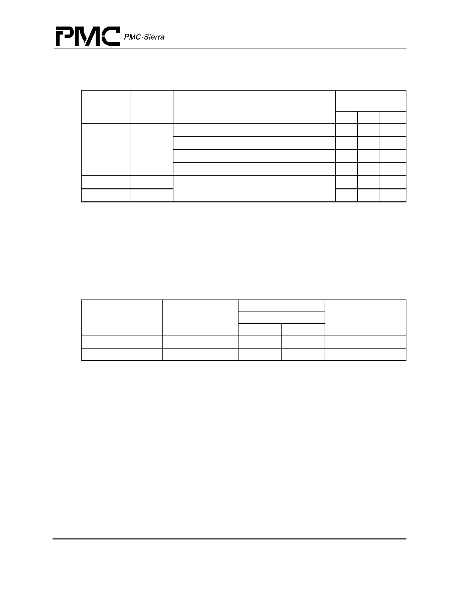
Absolute Maximum Ratings
1
Symbol
Rating
Limits
Unit
V
TERM
Terminal Voltage with respect to GND
≠0.5
2
to +3.9
V
T
CASE
Operating Temperature
Commercial
0 to +85
∞
C
Industrial
≠45 to +85
∞
C
T
STG
Storage Temperature
≠55 to +125
∞
C
I
IN
DC Input Current
±
20
3
mA
I
OUT
DC Output Current
±
20
4
mA
Notes
1.
Stresses greater than those listed under ABSOLUTE MAXIMUM RATINGS may cause permanent
damage to the device. This is a stress rating only and functional operation of the device at these or
any other conditions above those indicated in the operational sections of this specification is not
implied. Exposure to absolute maximum rating conditions for extended periods may affect reliability.
2.
V
IN
minimum = -2.0 V for pulse width less than 15 ns. V
IN
should not exceed 3.9 V.
3.
When V
IN
< 0V or V
IN
> VccIO.
4.
Not more than one output should be shorted at a time. Duration of the short should not exceed 30
seconds.

Proprietary and Confidential to PMC-Sierra, Inc and for its Customer's Internal Use
30
Document ID: PMC-2002165, Issue 1
RM5231TM Microprocessor with 32-bit System Bus Data Sheet
Released
6
Recommended Operating Conditions
Notes
1.
VccIO should not exceed VccInt by greater than 1.2 V during the power-up sequence.
2.
Applying a logic high state to any I/O pin before VccInt becomes stable is not recommended.
3.
As specified in IEEE 1149.1 (JTAG), the JTMS pin must be held high during reset to avoid entering JTAG
test mode.
4.
VccP must be connected to VccInt through a passive filter circuit. See the RM5200 User's Manual for
the recommended filter circuit.
Grade
Temperature
Vss
VccInt
VccIO
VccP
Commercial
0
∞
C to +85
∞
C (Case)
0 V
2.5 V
±
5%
3.15 V ≠ 3.45 V
2.5 V
±
5%
Industrial
-40
∞
C to +85
∞
C (Case)
0 V
2.5 V
±
5%
3.15 V ≠ 3.45 V
2.5 V
±
5%
Proprietary and Confidential to PMC-Sierra, Inc and for its Customer's Internal Use
31
Document ID: PMC-2002165, Issue 1
RM5231TM Microprocessor with 32-bit System Bus Data Sheet
Released
7
DC Electrical Characteristics
Parameter
Minimum
Maximum
Conditions
V
OL
0.2 V
|I
OUT
|= 100
µ
A
V
OH
VccIO - 0.2 V
V
OL
0.4 V
|I
OUT
| = 2 mA
V
OH
2.4 V
V
IL
-0.3 V
0.8 V
V
IH
2.0 V
VccIO + 0.3 V
I
IN
±1
5
µ
A
±1
5
µ
A
V
IN
=
0
V
IN
= VccIO

Proprietary and Confidential to PMC-Sierra, Inc and for its Customer's Internal Use
32
Document ID: PMC-2002165, Issue 1
RM5231TM Microprocessor with 32-bit System Bus Data Sheet
Released
8
Power Consumption
Parameter
Conditions:
Max: VccInt = 2.625
Typ: VccInt = 2.5 V
CPU Speed
150 MHz
200 MHz
250 MHz
Typ
1
Max
2
Typ
1
Max
2
Typ
1
Max
2
VccInt
Power
(mWatts)
standby
200
250
350
active
R4000 write protocol with no FPU
operation (integer instructions
only)
1100
2200
1425
2800
1725
3450
Write re-issue or pipelined writes
with superscalar
1225
2450
1600
3200
1900
3800
Notes
1.
Typical integer instruction mix with nominal supply voltage (untested).
2.
Worst case instruction mix with maximum supply voltage.
3.
I/O supply power is application dependant, but typically <20% of VccInt.

Proprietary and Confidential to PMC-Sierra, Inc and for its Customer's Internal Use
33
Document ID: PMC-2002165, Issue 1
RM5231TM Microprocessor with 32-bit System Bus Data Sheet
Released
9
AC Electrical Characteristics
9.1
Capacitive Load Deration
9.2
Clock Parameters
Parameter
Symbol
CPU Speed
Units
150≠250 MHz
Min
Max
Load Derate
C
LD
2
ns/25 pF
IO Power Derate
17.5
mW/25 pF/ MHz
IO Power Derate @ 20 pF Load
4.0
5.5
mW/ MHz
Parameter
Symbol
Test
Conditions
CPU Speed
Units
150 MHz
200 MHz
250 MHz
Min
Max
Min
Max
Min
Max
SysClock High
t
SCH
Transition
5 ns 3
3
3
ns
SysClock Low
t
SCL
Transition
5 ns 3
3
3
ns
SysClock Frequency
25
75
25
100
25
100
MHz
SysClock Period
t
SCP
40
40
40
ns
Clock Jitter for SysClock
t
JI
±
200
±
200
±
150
ps
SysClock Rise Time
t
CR
2
2
2
ns
SysClock Fall Time
t
CF
2
2
2
ns
ModeClock Period
t
ModeCKP
256
256
256
t
SCP
JTAG Clock Period
t
JTAGCKP
4
4
4
t
SCP
Note
1.
Operation of the RM5231 is only guaranteed with the Phase Lock Loop enabled.
Proprietary and Confidential to PMC-Sierra, Inc and for its Customer's Internal Use
34
Document ID: PMC-2002165, Issue 1
RM5231TM Microprocessor with 32-bit System Bus Data Sheet
Released
9.3
System Interface Parameters
1
9.4
Boot-Time Interface Parameters
Parameter
Symbol
Conditions
150≠250 MHz CPU
Speed
Min
Max
Units
Data Output
2,3
t
DO
mode14..13 = 10 (fastest)
5
1.0
4.5
ns
mode14..13 = 11
5
1.0
5.0
ns
mode14..13 = 00
5
1.0
5.5
ns
mode14..13 = 01 (slowest)
5
1.0
6.0
ns
Data Setup
4
t
DS
t
rise
= see above table
t
fall
= see above table
2.5
ns
Data Hold
4
t
DH
1.0
ns
Notes
1.
Timings are measured from 1.5 V of the clock to 1.5 V of the signal.
2.
Capacitive load for all maximum output timings is 50 pF. Minimum output timings are for a theoretical no
load condition - untested.
3.
Data Output timing applies to all signal pins whether tristate I/O or output only.
4.
Setup and Hold parameters apply to all signal pins whether tristate I/O or input only.
5.
Only mode 14:13 = 00 is tested and guaranteed.
Parameter
Symbol
CPU Speed
Units
150≠250 MHz
Min
Max
Mode Data Setup
t
DS
(M)
4
SysClock cycles
Mode Data Hold
t
DH
(M)
0
SysClock cycles

Proprietary and Confidential to PMC-Sierra, Inc and for its Customer's Internal Use
35
Document ID: PMC-2002165, Issue 1
RM5231TM Microprocessor with 32-bit System Bus Data Sheet
Released
10
Timing Diagrams
Figure 9 Clock Timing
10.1 System Interface Timing
(SysAD, SysCmd, ValidIn*, ValidOut*, etc.)
Figure 10 Input Timing
Figure 11 Output Timing
SysClock
t
Rise
t
Fall
t
High
t
Low
±t
JitterIn
t
DS
t
DH
Data
SysClock
Data
t
DOmin
t
DOmax
SysClock
Data
Data
Data

Proprietary and Confidential to PMC-Sierra, Inc and for its Customer's Internal Use
36
Document ID: PMC-2002165, Issue 1
RM5231TM Microprocessor with 32-bit System Bus Data Sheet
Released
11
Packaging Information
BOTTOM VIEW
ODD LEAD SIDES
(b)
X 3
X = A, B, OR D
EVEN LEAD SIDES
e/2
DETAIL "A"
X 3
X = A, B, OR D
GAGE PLANE
0.25
0-7
∞
1.60 REF.
L
C
C
0.13/0.30 R
DETAIL "B"
A1 13
A2
2 H
0.40 MIN.
0.13
R. MIN.
SECTION C-C
WITH LEAD FINISH
BASE METAL
0.13/0.19
11
0.13/0.23
8
b
b
1
SEATING
PLANE
C
A
SEE DETAIL "B"
12-16
∞
e
b
(N-4)X
D
A-B
C
8
TOP VIEW
4.00 R.
4 PLACES
B 3
11.0 REF.
0.20 C A-BD
4X
11.0 REF.
SEE
DETAIL "A"
4
D
D/2
A 3
2.00 DIA 4 PLACES
E/2
D 3
E 4
7
5
DA-B H 0.20
4X
0.10
11
11
11
0.076 C
D1/2
D1
5
7
(D2)
11.0 REF.
(E2)
"COUNTRY OF ORIGIN" MARK
3.00 REF. DIA. 4 PLACES
E1/2
E1
11.0 REF.
0
∞
MIN.
Hx
Hy
10
a,a,a
M
All dimensions are in millimeters unless otherwise noted.
1
128
Pin #1 I.D.
Symbol
Min
Nominal
Max
Note
A
--
3.70
4.07
A1
0.25
0.33
--
A2
3.17
3.37
3.67
D
31.20 BSC
To be determined at seating Plane C.
D1
28.00 BSC
Dimensions D1 and E1 do not include mold protrusion.
Allowable mold protrusion is 0.254 MM per side. Dimension
D1 and E1 do include mold mismatch and are determined at
Datum Plane H.
D2
24.00 REF.
E
31.20 BSC
To be determined at seating Plane C.
E1
28.00 BSC
Dimensions D1 and E1 do not include mold protrusion.
Allowable mold protrusion is 0.254 MM per side. Dimension
D1 and E1 do include mold mismatch and are determined at
Datum Plane H.
E2
24.00 REF.
D3
21.0 REF.
E3
21.0 REF.
L
0.65
0.70
0.95
e
0.80 BSC
b
0.30
--
0.45

Proprietary and Confidential to PMC-Sierra, Inc and for its Customer's Internal Use
37
Document ID: PMC-2002165, Issue 1
RM5231TM Microprocessor with 32-bit System Bus Data Sheet
Released
Notes
b1
0.30
0.35
0.40
a,a,a
0.16
ThetaJa
13.7
∞
C/W
ThetaJc
1.5
∞
C/W
Symbol
Min
Nominal
Max
Note
1.
All dimensioning and tolerances confirm to ASME Y14.5≠1994.
2.
Datum Plane H located at the bottom of the mold parting line and coincident with where lead exits plastic
body.
3.
Datums A≠B and D to be determined where center line between leads exits plastic body at Datum Plane
H.
4.
To be determined at seating Plane C.
5.
Dimensions D1 and E1 do not include mold protrusion. Allowable mold protrusion is 0.254 MM per side.
Dimension D1 and E1 do include mold mismatch and are determined at Datum Plane H.
6.
"N" is number of terminals.
7.
Package top dimensions are smaller than bottom dimensions by 0.20 millimeters and top of package will
not overhang bottom of package.
8.
Dimensions b does not include Damabr protrusion. Allowable Damabr protrusion shall be 0.08 MM. Total
in excess of b dimension at maximum material condition. Damabr can not be located on the lower radius
or the foot. The dimension space between protrusion and an adjacent lead shall not be less than 0.07
MM for 0.4 MM and 0.50 MM pitch package.
9.
All dimensions are in millimeters.
10. The optional exposed heat shrink is coincident with the top or bottom side of the package and not
allowed to protrude beyond that surface.
11. These dimensions apply to the flat section of the lead between 0.10 MM and 0.25 MM from the lead tip.
12. This drawing conforms to JEDEC registered outline MS-022. But the heat slug dimension was not
specified on JEDEC.
13. A1 is defined as the distance from the seating plane to the lowest point of the package body.

Proprietary and Confidential to PMC-Sierra, Inc and for its Customer's Internal Use
38
Document ID: PMC-2002165, Issue 1
RM5231TM Microprocessor with 32-bit System Bus Data Sheet
Released
12
RM5231 128 PQFP Package Pinout
Pin
Function
Pin
Function
Pin
Function
Pin
Function
1
NC
33
ModeIn
65
NMI*
97
NC
2
NC
34
RdRdy*
66
ExtRqst*
98
NC
3
VccIO
35
WrRdy*
67
Reset*
99
NC
4
Vss
36
ValidIn*
68
ColdReset*
100
NC
5
SysAD4
37
ValidOut*
69
VccOK
101
VccIO
6
SysAD5
38
Release*
70
BigEndian
102
Vss
7
VccInt
39
VccP
71
VccIO
103
SysAD28
8
Vss
40
VssP
72
Vss
104
SysAD29
9
SysAD6
41
SysClock
73
SysAD16
105
VccInt
10
SysAD7
42
VccInt
74
VccInt
106
Vss
11
SysAD8
43
Vss
75
Vss
107
SysAD30
12
SysAD9
44
SysCmd0
76
SysAD17
108
SysAD31
13
VccIO
45
SysCmd1
77
SysAD18
109
SysADC2
14
Vss
46
SysCmd2
78
SysAD19
110
VccInt
15
SysAD10
47
SysCmd3
79
VccInt
111
Vss
16
SysAD11
48
VccIO
80
Vss
112
SysADC3
17
VccInt
49
Vss
81
SysAD20
113
VccIO
18
Vss
50
SysCmd4
82
SysAD21
114
Vss
19
SysAD12
51
SysCmd5
83
VccIO
115
SysADC0
20
SysAD13
52
Vss
84
Vss
116
SysADC1
21
SysAD14
53
SysCmd6
85
SysAD22
117
SysAD0
22
VccInt
54
SysCmd7
86
SysAD23
118
SysAD1
23
Vss
55
SysCmd8
87
SysAD24
119
VccInt
24
SysAD15
56
SysCmdP
88
SysAD25
120
Vss
25
VccIO
57
VccInt
89
VccInt
121
SysAD2
26
Vss
58
Vss
90
Vss
122
SysAD3
27
ModeClock
59
Int0*
91
SysAD26
123
VccIO
28
JTDO
60
Int1*
92
SysAD27
124
Vss
29
JTDI
61
Int2*
93
VccIO
125
NC
30
JTCK
62
Int3*
94
Vss
126
NC
31
JTMS
63
Int4*
95
NC
127
NC
32
VccIO
64
Int5*
96
NC
128
NC

Proprietary and Confidential to PMC-Sierra, Inc and for its Customer's Internal Use
39
Document ID: PMC-2002165, Issue 1
RM5231TM Microprocessor with 32-bit System Bus Data Sheet
Released
13
Ordering Information
Valid Combinations
RM5231≠150≠Q
RM5231≠200≠Q
RM5231≠250≠Q
RM5231≠200≠QI (Contact Sales prior to design)
RM5231
-123
A
I
Temperature Grade:
(blank) = commercial
I = Industrial
Package Type:
Q = Power Quad 4 (PQ-4)
Device Maximum Speed
Device Type