Document Outline
- TITLE PAGE
- Revision History
- Legal Information
- Revision History
- Document Conventions
- Table of Contents
- List of Figures
- List of Tables
- 1 Features
- 2 Block Diagram
- 3 Description
- 4 Hardware Overview
- 4.1 CPU Registers
- 4.2 Superscalar Dispatch
- Table 1 Instruction Issue Rules
- Figure 3 Instruction Issue Paradigm
- Table 2 Dual Issue Instruction Classes
- add, sub, or, xor, shift, etc.
- lw, sw, ld, sd, ldc1, sdc1, mov, movc, fmov, etc.
- fadd, fsub, fmult, fmadd, fdiv, fcmp, fsqrt, etc.
- beq, bne, bCzT, bCzF, j, etc.
- 4.3 Pipeline
- 4.4 Integer Unit
- 4.5 ALU
- 4.6 Integer Multiply/Divide
- 4.7 Floating-Point Coprocessor
- 4.8 Floating-Point Unit
- 4.9 Floating-Point General Register File
- 4.10 System Control Coprocessor (CP0)
- 4.11 System Control Coprocessor Registers
- 4.12 Virtual to Physical Address Mapping
- 4.13 Joint TLB
- 4.14 Instruction TLB
- 4.15 Data TLB
- 4.16 Cache Memory
- 4.17 Instruction Cache
- 4.18 Data Cache
- 4.19 Secondary Cache
- 4.20 Secondary Caching Protocols
- 4.21 Tertiary Cache
- 4.22 Cache Locking
- 4.23 Cache Management
- 4.24 Primary Write Buffer
- 4.25 System Interface
- 4.26 System Address/Data Bus
- 4.27 System Command Bus
- 4.28 Handshake Signals
- 4.29 System Interface Operation
- 4.30 Data Prefetch
- 4.31 Enhanced Write Modes
- 4.32 External Requests
- 4.33 Test/Breakpoint Registers
- 4.34 Performance Counters
- 4.35 Interrupt Handling
- 4.36 Standby Mode
- 4.37 JTAG Interface
- 4.38 Boot-Time Options
- 4.39 Boot-Time Modes
- 5 Pin Descriptions
- 6 Absolute Maximum Ratings1
- 7 Recommended Operating Conditions
- 8 DC Electrical Characteristics
- 9 Power Consumption
- 10 AC Electrical Characteristics
- 11 Timing Diagrams
- 12 Packaging Information
- 13 RM7000 Pinout
- 14 Ordering Information

Proprietary and Confidential to PMC-Sierra, Inc and for its Customer's Internal Use
Document ID: PMC-2002175, Issue 1
RM7000TM Microprocessor with On-Chip Secondary Cache Datasheet
Released
RM7000
RM7000TM Microprocessor with On-Chip
Secondary Cache
Datasheet
Proprietary and Confidential
Issue 1, January 2001

Proprietary and Confidential to PMC-Sierra, Inc and for its Customer's Internal Use
2
Document ID: PMC-2002175, Issue 1
RM7000TM Microprocessor with On-Chip Secondary Cache Datasheet
Released
Legal Information
Copyright
© 2001 PMC-Sierra, Inc.
The information is proprietary and confidential to PMC-Sierra, Inc., and for its customers' internal
use. In any event, you cannot reproduce any part of this document, in any form, without the
express written consent of PMC-Sierra, Inc.
PMC-2002175 (R1)
Disclaimer
None of the information contained in this document constitutes an express or implied warranty by
PMC-Sierra, Inc. as to the sufficiency, fitness or suitability for a particular purpose of any such
information or the fitness, or suitability for a particular purpose, merchantability, performance,
compatibility with other parts or systems, of any of the products of PMC-Sierra, Inc., or any
portion thereof, referred to in this document. PMC-Sierra, Inc. expressly disclaims all
representations and warranties of any kind regarding the contents or use of the information,
including, but not limited to, express and implied warranties of accuracy, completeness,
merchantability, fitness for a particular use, or non-infringement.
In no event will PMC-Sierra, Inc. be liable for any direct, indirect, special, incidental or
consequential damages, including, but not limited to, lost profits, lost business or lost data
resulting from any use of or reliance upon the information, whether or not PMC-Sierra, Inc. has
been advised of the possibility of such damage.
Trademarks
RM7000 and Fast Packet Cache are trademarks of PMC-Sierra, Inc.
Contacting PMC-Sierra
PMC-Sierra, Inc.
105-8555 Baxter Place Burnaby, BC
Canada V5A 4V7
Tel: (604) 415-6000
Fax: (604) 415-6200
Document Information: document@pmc-sierra.com
Corporate Information: info@pmc-sierra.com
Technical Support: apps@pmc-sierra.com
Web Site: http://www.pmc-sierra.com
Proprietary and Confidential to PMC-Sierra, Inc and for its Customer's Internal Use
3
Document ID: PMC-2002175, Issue 1
RM7000TM Microprocessor with On-Chip Secondary Cache Datasheet
Released
Revision History
Issue
No.
Issue Date
ECN
Number
Originator
Details of Change
1
January 2001
3618
T. Chapman
Applied PMC-Sierra template to existing
MPD (QED) FrameMaker document.
Changed IP register bits to INT.
Updated Notes 1 and 5 of the System
Interface Parameters table.

Proprietary and Confidential to PMC-Sierra, Inc and for its Customer's Internal Use
4
Document ID: PMC-2002175, Issue 1
RM7000TM Microprocessor with On-Chip Secondary Cache Datasheet
Released
Document Conventions
The following conventions are used in this datasheet:
∑
All signal, pin, and bus names described in the text, such as ExtRqst*, are in boldface
typeface.
∑
All bit and field names described in the text, such as Interrupt Mask, are in an italic-
bold typeface.
∑
All instruction names, such as
MFHI
, are in san serif typeface.

Proprietary and Confidential to PMC-Sierra, Inc and for its Customer's Internal Use
5
Document ID: PMC-2002175, Issue 1
RM7000TM Microprocessor with On-Chip Secondary Cache Datasheet
Released
Table of Contents
Legal Information ...........................................................................................................................2
Revision History .............................................................................................................................3
Document Conventions .................................................................................................................4
Table of Contents ..........................................................................................................................5
List of Figures ................................................................................................................................7
List of Tables .................................................................................................................................8
1
Features ..................................................................................................................................9
2
Block Diagram .......................................................................................................................10
3
Description ............................................................................................................................11
4
Hardware Overview ...............................................................................................................12
4.1
CPU Registers .............................................................................................................12
4.2
Superscalar Dispatch ...................................................................................................12
4.3
Pipeline ........................................................................................................................13
4.4
Integer Unit ..................................................................................................................14
4.5
ALU ..............................................................................................................................15
4.6
Integer Multiply/Divide ..................................................................................................15
4.7
Floating-Point Coprocessor ..........................................................................................16
4.8
Floating-Point Unit .......................................................................................................16
4.9
Floating-Point General Register File ............................................................................16
4.10 System Control Coprocessor (CP0) .............................................................................17
4.11 System Control Coprocessor Registers .......................................................................18
4.12 Virtual to Physical Address Mapping ............................................................................19
4.13 Joint TLB ......................................................................................................................20
4.14 Instruction TLB .............................................................................................................20
4.15 Data TLB ......................................................................................................................20
4.16 Cache Memory .............................................................................................................21
4.17 Instruction Cache .........................................................................................................21
4.18 Data Cache ..................................................................................................................21
4.19 Secondary Cache ........................................................................................................23
4.20 Secondary Caching Protocols ......................................................................................24
4.21 Tertiary Cache .............................................................................................................24
4.22 Cache Locking .............................................................................................................26
4.23 Cache Management .....................................................................................................26
4.24 Primary Write Buffer .....................................................................................................27
4.25 System Interface ..........................................................................................................27
4.26 System Address/Data Bus ...........................................................................................28
4.27 System Command Bus ................................................................................................28
4.28 Handshake Signals ......................................................................................................28
4.29 System Interface Operation .........................................................................................29

Proprietary and Confidential to PMC-Sierra, Inc and for its Customer's Internal Use
6
Document ID: PMC-2002175, Issue 1
RM7000TM Microprocessor with On-Chip Secondary Cache Datasheet
Released
4.30 Data Prefetch ...............................................................................................................31
4.31 Enhanced Write Modes ................................................................................................32
4.32 External Requests ........................................................................................................32
4.33 Test/Breakpoint Registers ............................................................................................32
4.34 Performance Counters .................................................................................................33
4.35 Interrupt Handling ........................................................................................................35
4.36 Standby Mode ..............................................................................................................37
4.37 JTAG Interface .............................................................................................................37
4.38 Boot-Time Options .......................................................................................................37
4.39 Boot-Time Modes .........................................................................................................37
5
Pin Descriptions ....................................................................................................................39
6
Absolute Maximum Ratings1 ................................................................................................43
7
Recommended Operating Conditions ...................................................................................44
8
DC Electrical Characteristics .................................................................................................45
9
Power Consumption ..............................................................................................................46
10 AC Electrical Characteristics .................................................................................................47
10.1 Capacitive Load Deration .............................................................................................47
10.2 Clock Parameters ........................................................................................................47
10.3 System Interface Parameters ......................................................................................48
10.4 Boot-Time Interface Parameters ..................................................................................48
11 Timing Diagrams ...................................................................................................................49
11.1 Clock Timing ................................................................................................................49
12 Packaging Information ..........................................................................................................50
13 RM7000 Pinout .....................................................................................................................51
14 Ordering Information .............................................................................................................53

RM7000ATM Microprocessor with On-Chip Secondary Cache Datasheet
Proprietary and Confidential to PMC-Sierra, Inc and for its Customer's Internal Use
7
Document ID: PMC-2002175, Issue 1
Released
List of Figures
Figure 1
Block Diagram ..........................................................................................................10
Figure 2
CP0 Registers ...........................................................................................................12
Figure 3
Instruction Issue Paradigm .......................................................................................13
Figure 4
Pipeline 1 ...................................................................................................................4
Figure 5
CP0 Registers ...........................................................................................................18
Figure 6
Kernel Mode Virtual Addressing (32-bit mode) .........................................................19
Figure 7
Tertiary Cache Hit and Miss .....................................................................................25
Figure 8
Typical Embedded System Block Diagram ...............................................................28
Figure 9
Processor Block Read ..............................................................................................30
Figure 10 Processor Block Write ..............................................................................................31
Figure 11 Multiple Outstanding Reads ......................................................................................31
Figure 12 Clock Timing .............................................................................................................49
Figure 13 Input Timing ..............................................................................................................49
Figure 14 Output Timing ...........................................................................................................49

RM7000ATM Microprocessor with On-Chip Secondary Cache Datasheet
Proprietary and Confidential to PMC-Sierra, Inc and for its Customer's Internal Use
8
Document ID: PMC-2002175, Issue 1
Released
List of Tables
Table 1
Instruction Issue Rules ...............................................................................................12
Table 2
Dual Issue Instruction Classes ...................................................................................13
Table 3
ALU Operations .........................................................................................................15
Table 4
Integer Multiply/Divide Operations ..............................................................................15
Table 5
Floating Point Latencies and Repeat Rates ...............................................................17
Table 6
Cache Attributes .........................................................................................................26
Table 7
Cache Locking Control ...............................................................................................26
Table 8
Penalty Cycles ............................................................................................................27
Table 9
Watch Control Register ...............................................................................................33
Table 10 Performance Counter Control .....................................................................................34
Table 11 Cause Register ...........................................................................................................36
Table 12 Interrupt Control Register ...........................................................................................36
Table 13 IPLLO Register ...........................................................................................................36
Table 14 IPLHI Register ............................................................................................................36
Table 15 Interrupt Vector Spacing .............................................................................................37
Table 16 Boot Time Mode Stream .............................................................................................38
Table 17 System interface Pins .................................................................................................39
Table 18 Clock/control interface Pins ........................................................................................40
Table 19 Tertiary cache interfacePins .......................................................................................41
Table 20 Interrupt Interface Pins ...............................................................................................42
Table 21 JTAG Interface Pins ....................................................................................................42
Table 22 Initialization Interface Pins ..........................................................................................42

Proprietary and Confidential to PMC-Sierra, Inc and for its Customer's Internal Use
9
Document ID: PMC-2002175, Issue 1
RM7000TM Microprocessor with On-Chip Secondary Cache Datasheet
Released
1
Features
∑
Dual Issue symmetric superscalar microprocessor with instruction prefetch optimized for
system level price/performance
∑
200, 250, 266, 300 MHz operating frequency
∑
>500 Dhrystone 2.1 MIPS @ 300 MHz
∑
High-performance system interface
∑
1000 MB per second peak throughput
∑
125 MHz max. freq., multiplexed address/data
∑
Supports two outstanding reads with out-of-order return
∑
Processor clock multipliers 2, 2.5, 3, 3.5, 4, 4.5, 5, 6, 7, 8, 9
∑
Integrated primary and secondary caches -- all are 4-way set associative with 32 byte line size
∑
16 KB instruction, 16 KB data, 256 KB on-chip secondary
∑
Per line cache locking in primaries and secondary
∑
Fast Packet CacheTM increases system efficiency in
networking applications
∑
Integrated external cache controller (up to 8 MB)
∑
High-performance floating-point unit -- 600 MFLOPS maximum
∑
Single cycle repeat rate for common single-precision operations and some double-pre-
cision operations
∑
Single cycle repeat rate for single-precision combined multiply-add operations
∑
Two cycle repeat rate for double-precision multiply and double-precision combined
multiply-add operations
∑
MIPS IV Superset Instruction Set Architecture
∑
Data
PREFETCH
instruction allows the processor to overlap cache miss latency and
instruction execution
∑
Single-cycle floating-point multiply-add
∑
Integrated memory management unit
∑
Fully associative joint TLB (shared by I and D translations)
∑
64/48 dual entries map 128/96 pages
∑
Variable page size
∑
Embedded application enhancements
∑
Specialized DSP integer Multiply-Accumulate instructions, (
MAD
/
MADU
) and three-
operand multiply instruction (
MUL
)
∑
I&D Test/Break-point (Watch) registers for emulation & debug
∑
Performance counter for system and software tuning & debug
∑
Fourteen fully prioritized vectored interrupts - 10 external, 2 internal, 2 software
∑
Fully static CMOS design with dynamic power down logic
∑
RM5271 pin compatible, 304 pin TBGA package, 31x31 mm
Proprietary and Confidential to PMC-Sierra, Inc and for its Customer's Internal Use
10
Document ID: PMC-2002175, Issue 1
RM7000TM Microprocessor with On-Chip Secondary Cache Datasheet
Released
2
Block Diagram
Figure 1 Block Diagram
F Pipe
M Pipe
Instruction Dispatch Unit
Secondary Tags
Set A
Secondary Tags
Set B
Secondary Tags
Set D
Secondary Tags
Set C
Primary Data Cache
4-way Set Associative
Primary Instruction Cache
4-way Set Associative
DTag
DTLB
ITag
ITLB
Prefetch Buffer
F Pipe Register
M Pipe Register
Store Buffer
Write Buffer
Read Buffer
Pad Buffer
Address Buffer
Load Aligner
Integer Register File
Adder
DTLB Virtual
StAln/Sh
Logicals
PLL/Clocks
Floating-Point
Load/Align
Floating-Point
Register File
Packer/Unpacker
Comparator
Floating-Point
MultAdd, Add, Sub,
Cvt, Div, Sqrt
Multiplier Array
Joint TLB
Coprocessor 0
System/Memory
Control
PC Incrementer
Branch PC Adder
ITLB Virtual
Program Counter
Int Mult, Div, Madd
Floating-Point Control
Integer Control
DVA
IVA
Extenal Cache Controller
On-chip 256K Byte Secondary Cache, 4-way Set Associative
Adder
Shifter
Logicals
Pad Bus
D Bus
F-Pipe Bus
M-Pipe Bus
FA Bus
A/D Bus

Proprietary and Confidential to PMC-Sierra, Inc and for its Customer's Internal Use
11
Document ID: PMC-2002175, Issue 1
RM7000TM Microprocessor with On-Chip Secondary Cache Datasheet
Released
3
Description
PMC-Sierra's RM7000 is a highly integrated symmetric superscalar microprocessor capable of
issuing two instructions each processor cycle. It has two high-performance 64-bit integer units as
well as a high-throughput, fully pipelined 64-bit floating point unit. To keep its multiple execution
units running efficiently, the RM7000 integrates not only 16 KB 4-way set associative instruction
and data caches but backs them up with an integrated 256 KB 4-way set associative secondary as
well. For maximum efficiency, the data and secondary caches are write-back and non-blocking. An
optional external tertiary cache provides high-performance capability even in applications having
very large data sets.
A RM5200 Family compatible, operating system friendlymemory management unit with a 64/48-
entry fully associative TLB and a high-performance 64-bit system interface supporting multiple
outstanding reads with out-of-order return and hardware prioritized and vectored interrupts round
out the main features of the processor.
The RM7000 is ideally suited for high-end embedded control applications such as
internetworking, high-performance image manipulation, high-speed printing, and 3-D
visualization. The RM7000 is also applicable to the low end workstation market where its
balanced integer and floating-point performance and direct support for a large tertiary cache (up to
8 MB) provide outstanding price/performance.
Proprietary and Confidential to PMC-Sierra, Inc and for its Customer's Internal Use
12
Document ID: PMC-2002175, Issue 1
RM7000TM Microprocessor with On-Chip Secondary Cache Datasheet
Released
4
Hardware Overview
The RM7000 offers a high-level of integration targeted at high-performance embedded
applications. The key elements of the RM7000 are briefly described below.
4.1
CPU Registers
Like all MIPS ISA processors, the RM7000 CPU has a simple, clean user visible state consisting
of 32 general purpose registers (GPR), two special purpose registers for integer multiplication and
division, and a program counter; there are no condition code bits. Figure 2 shows the user visible
state.
Figure 2 CP0 Registers
4.2
Superscalar Dispatch
The RM7000 has an efficient symmetric superscalar dispatch unit which allows it to issue up to
two instructions per cycle. For purposes of instruction issue, the RM7000 defines four classes of
instructions: integer, load/store, branches, and floating-point. There are two logical pipelines, the
function, or F, pipeline and the memory, or M, pipeline. Note however that the M pipe can execute
integer as well as memory type instructions.
Table 1 Instruction Issue Rules
Figure 3 is a simplification of the pipeline section and illustrates the basics of the instruction issue
mechanism.
General Purpose Registers
63
0
Multiply/Divide Registers
0
63
0
r1
HI
r2
63
0
∑
LO
∑
∑
Program Counter
∑
63
0
r29
PC
r30
r31
F Pipe
M Pipe
one of:
one of:
integer, branch, floating-point,
integer mul, div
integer, load/store
Proprietary and Confidential to PMC-Sierra, Inc and for its Customer's Internal Use
13
Document ID: PMC-2002175, Issue 1
RM7000TM Microprocessor with On-Chip Secondary Cache Datasheet
Released
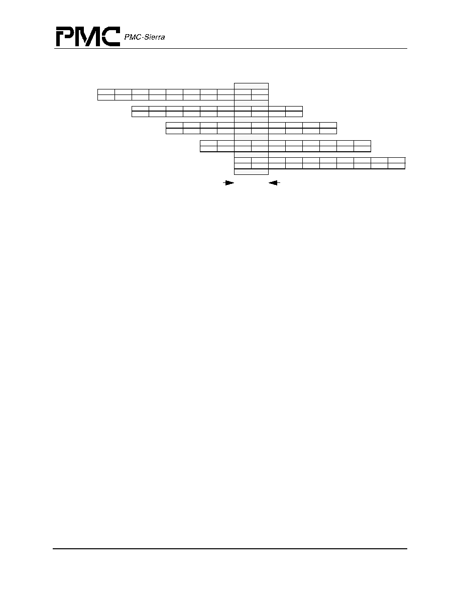
Figure 3 Instruction Issue Paradigm
The figure illustrates that one F pipe instruction and one M pipe instruction can be issued
concurrently but that two M pipe or two F pipe instructions cannot be issued. Table 2 specifies
more completely the instructions within each class.
Table 2 Dual Issue Instruction Classes
The symmetric superscalar capability of the RM7000, in combination with its low latency integer
execution units and high-throughput fully pipelined floating-point execution unit, provides
unparalleled price/performance in computational intensive embedded applications.
4.3
Pipeline
The logical length of both the F and M pipelines is five stages with state committing in the register
write, or W, pipe stage. The physical length of the floating-point execution pipeline is actually
seven stages but this is completely transparent to the user.
Figure 4 shows instruction execution within the RM7000 when instructions are issuing
simultaneously down both pipelines. As illustrated in the figure, up to ten instructions can be
executing simultaneously. This figure presents a somewhat simplistic view of the processors
operation however since the out-of-order completion of loads, stores, and long latency floating-
point operations can result in there being even more instructions in process than what is shown.
integer
load/store
floating-point
branch
add, sub, or, xor, shift,
etc.
lw, sw, ld, sd, ldc1,
sdc1, mov, movc,
fmov, etc.
fadd, fsub, fmult,
fmadd, fdiv, fcmp,
fsqrt, etc.
beq, bne, bCzT,
bCzF, j, etc.
F Pipe
Integer
M Pipe
Integer
F Pipe
FP
M Pipe
FP
Cache
Instruction
Unit
Dispatch
F Pipe IBus
M Pipe IBus
Proprietary and Confidential to PMC-Sierra, Inc and for its Customer's Internal Use
14
Document ID: PMC-2002175, Issue 1
RM7000TM Microprocessor with On-Chip Secondary Cache Datasheet
Released
Figure 4 Pipeline
Note that instruction dependencies, resource conflicts, and branches result in some of the
instruction slots being occupied by
NOP
s.
4.4
Integer Unit
Like the RM5200 Fcamily, the RM7000 implements the MIPS IV Instruction Set Architecture,
and is therefore fully upward compatible with applications that run on processors such as the
R4650 and R4700 that implement the earlier generation MIPS III Instruction Set Architecture.
Additionally, the RM7000 includes two implementation specific instructions not found in the
baseline MIPS IV ISA, but that are useful in the embedded market place. Described in detail in a
later section, these instructions are integer multiply-accumulate and three-operand integer
multiply.
The RM7000 integer unit includes thirty-two general purpose 64-bit registers, the HI/LO result
registers for the two-operand integer multiply/divide operations, and the program counter, or PC.
There are two separate execution units, one of which can execute function, or F, type instructions
and one which can execute memory, or M, type instructions. See above for a description of the
instruction types and the issue rules. As a special case, integer multiply/divide instructions as well
as their corresponding
MFHI
and
MFLO
instructions can only be executed in the F type
execution unit. Within each execution unit the operational characteristics are the same as on
previous MIPS designs with single cycle ALU operations (add, sub, logical, shift), one cycle load
delay, and an autonomous multiply/divide unit.
Register File
The RM7000 has thirty-two general purpose registers with register location 0 (r0) hard wired to a
zero value. These registers are used for scalar integer operations and address calculation. In order
to service the two integer execution units, the register file has four read ports and two write ports
and is fully bypassed both within and between the two execution units to minimize operation
latency in the pipeline.
I0
I2
I4
I6
I8
2I
1I
1R
2R
1A
2A
1D
2D
1W
2W
2I
1I
1R
2R
1A
2A
1D
2D
1W
2W
2I
1I
1R
2R
1A
2A
1D
2D
1W
2W
2I
1I
1R
2R
1A
2A
1D
2D
1W
2W
2I
1I
1R
2R
1A
2A
1D
2D
1W
2W
one cycle
1I-1R:
2I:
2A-2D:
2R:
1A-2A:
1A:
1A:
1D:
2A:
2W:
Instruction cache access
Instruction virtual to physical address translation
Register file read, Bypass calculation, Instruction decode, Branch address calculation
Issue or slip decision, Branch decision
Integer add, logical, shift
Data virtual address calculation
Data virtual to physical address translation
Store Align
Register file write
Data cache access and load align
I1
2I
1I
1R
2R
1A
2A
1D
2D
1W
2W
I3
2I
1I
1R
2R
1A
2A
1D
2D
1W
2W
I5
2I
1I
1R
2R
1A
2A
1D
2D
1W
2W
I7
2I
1I
1R
2R
1A
2A
1D
2D
1W
2W
I9
2I
1I
1R
2R
1A
2A
1D
2D
1W
2W

Proprietary and Confidential to PMC-Sierra, Inc and for its Customer's Internal Use
15
Document ID: PMC-2002175, Issue 1
RM7000TM Microprocessor with On-Chip Secondary Cache Datasheet
Released
4.5
ALU
The RM7000 has two complete integer ALUs each consisting of an integer adder/subtractor, a
logic unit, and a shifter. Table 3 shows the functions performed by the ALUs for each execution
unit. Each of these units is optimized to perform all operations in a single processor cycle.
Table 3 ALU Operations
4.6
Integer Multiply/Divide
The RM7000 has a single dedicated integer multiply/divide unit optimized for high-speed multiply
and multiply-accumulate operations. The multiply/divide unit resides in the F type execution unit.
Table 4 shows the performance of the multiply/divide unit on each operation.
Table 4 Integer Multiply/Divide Operations
The baseline MIPS IV ISA specifies that the results of a multiply or divide operation be placed in
the Hi and Lo registers. These values can then be transferred to the general purpose register file
using the Move-from-Hi and Move-from-Lo (
MFHI
/
MFLO
) instructions.
In addition to the baseline MIPS IV integer multiply instructions, the RM7000 also implements the
3-operand multiply instruction, MUL. This instruction specifies that the multiply result go directly
to the integer register file rather than the Lo register. The portion of the multiply that would have
normally gone into the Hi register is discarded. For applications where it is known that the upper
half of the multiply result is not required, using the
MUL
instruction eliminates the necessity of
executing an explicit
MFLO
instruction.
Also included in the RM7000 are the multiply-add instructions
MAD/MADU
. This instruction
multiplies two operands and adds the resulting product to the current contents of the Hi and Lo
registers. The multiply-accumulate operation is the core primitive of almost all signal processing
Unit
F Pipe
M Pipe
Adder
add, sub
add, sub, data address
add
Logic
logic, moves, zero shifts
(nop)
logic, moves, zero shifts
(nop)
Shifter
non zero shift
non zero shift, store align
Opcode
Operand
Size
Latency
Repeat
Rate
Stall
Cycles
MULT/U,
MAD/U
16 bit
4
3
0
32 bit
5
4
0
MUL
16 bit
4
3
2
32 bit
5
4
3
DMULT,
DMULTU
any
9
8
0
DIV, DIVD
any
36
36
0
DDIV,
DDIVU
any
68
68
0

Proprietary and Confidential to PMC-Sierra, Inc and for its Customer's Internal Use
16
Document ID: PMC-2002175, Issue 1
RM7000TM Microprocessor with On-Chip Secondary Cache Datasheet
Released
algorithms allowing the RM7000 to eliminate the need for a separate DSP engine in many
embedded applications.
By pipelining the multiply-accumulate function and dynamically determining the size of the input
operands, the RM7000 is able to maximize throughput while still using an area efficient
implementation.
4.7
Floating-Point Coprocessor
The RM7000 incorporates a high-performance fully pipelined floating-point coprocessor which
includes a floating-point register file and autonomous execution units for multiply/add/convert and
divide/square root. The floating-point coprocessor is a tightly coupled co-execution unit, decoding
and executing instructions in parallel with, and in the case of floating-point loads and stores, in
cooperation with the M pipe of the integer unit. As described earlier, the superscalar capabilities of
the RM7000 allow floating-point computation instructions to issue concurrently with integer
instructions.
4.8
Floating-Point Unit
The RM7000 floating-point execution unit supports single and double precision arithmetic, as
specified in the IEEE Standard 754. The execution unit is broken into a separate divide/square root
unit and a pipelined multiply/add unit. Overlap of divide/square root and multiply/add is
supported.
The RM7000 maintains fully precise floating-point exceptions while allowing both overlapped
and pipelined operations. Precise exceptions are extremely important in object-oriented
programming environments and highly desirable for debugging in any environment.
The floating-point unit's operation set includes floating-point add, subtract, multiply, multiply-
add, divide, square root, reciprocal, reciprocal square root, conditional moves, conversion between
fixed-point and floating-point format, conversion between floating-point formats, and floating-
point compare. Table 5 gives the latencies of the floating-point instructions in internal processor
cycles.
4.9
Floating-Point General Register File
The floating-point general register file, FGR, is made up of thirty-two 64-bit registers. With the
floating-point load and store double instructions,
LDC1
and
SDC1
, the floating-point unit can
take advantage of the 64-bit wide data cache and issue a floating-point coprocessor load or store
doubleword instruction in every cycle.
The floating-point control register file contains two registers; one for determining configuration
and revision information for the coprocessor and one for control and status information. These
registers are primarily used for diagnostic software, exception handling, state saving and restoring,
and control of rounding modes.

Proprietary and Confidential to PMC-Sierra, Inc and for its Customer's Internal Use
17
Document ID: PMC-2002175, Issue 1
RM7000TM Microprocessor with On-Chip Secondary Cache Datasheet
Released
Table 5 Floating Point Latencies and Repeat Rates
To support superscalar operations, the FGR has four read ports and two write ports, and is fully
bypassed to minimize operation latency in the pipeline. Three of the read ports and one write port
are used to support the combined multiply-add instruction while the fourth read and second write
port allows a concurrent floating-point load or store and conditional moves.
4.10 System Control Coprocessor (CP0)
The system control coprocessor (CP0) in the MIPS architecture is responsible for the virtual
memory sub-system, the exception control system, and the diagnostics capability of the processor.
In the MIPS architecture, the system control coprocessor (and thus the kernel software) is
implementation dependent. For memory management, the RM7000 CP0 is logically identical to
that of the RM5200 Family and R5000. For interrupt exceptions and diagnostics, the RM7000 is a
superset of the RM5200 Family and R5000 implementing additional features described later in the
sections on Interrupts, the Test/Breakpoint facility, and the Performance Counter facility.
The memory management unit controls the virtual memory system page mapping. It consists of an
instruction address translation buffer (ITLB), a data address translation buffer (DTLB), a Joint
TLB (JTLB), and coprocessor registers used by the virtual memory mapping sub-system.
Operation
Latency
Single/double
Repeat Rate
Single/double
fadd
4
1
fsub
4
1
fmult
4/5
1/2
fmadd
4/5
1/2
fmsub
4/5
1/2
fdiv
21/36
19/34
fsqrt
21/36
19/34
frecip
21/36
19/34
frsqrt
38/68
36/66
fcvt.s.d
4
1
fcvt.s.w
6
3
fcvt.s.l
6
3
fcvt.d.s
4
1
fcvt.d.w
4
1
fcvt.d.l
4
1
fcvt.w.s
4
1
fcvt.w.d
4
1
fcvt.l.s
4
1
fcvt.l.d
4
1
fcmp
1
1
fmov, fmovc
1
1
fabs, fneg
1
1

Proprietary and Confidential to PMC-Sierra, Inc and for its Customer's Internal Use
18
Document ID: PMC-2002175, Issue 1
RM7000TM Microprocessor with On-Chip Secondary Cache Datasheet
Released
4.11 System Control Coprocessor Registers
The RM7000 incorporates all system control coprocessor (CP0) registers internally. These
registers provide the path through which the virtual memory system's page mapping is examined
and modified, exceptions are handled, and operating modes are controlled (kernel vs. user mode,
interrupts enabled or disabled, cache features). In addition, the RM7000 includes registers to
implement a real-time cycle counting facility, to aid in cache and system diagnostics, and to assist
in data error detection.
To support the non-blocking caches and enhanced interrupt handling capabilities of the RM7000,
both the data and control register spaces of CP0 are supported by the RM7000. In the data register
space, that is the space accessed using the
MFC0
and
MTC0
instructions, the RM7000 supports
the same registers as found in the RM5200, R4000 and R5000 families. In the control space, that is
the space accessed by the previously unused
CTC0
and
CFC0
instructions, the RM7000 supports
five new registers. The first three of these new 32-bit registers support the enhanced interrupt
handling capabilities and are the Interrupt Control, Interrupt Priority Level Lo (IPLLO), and
Interrupt Priority Level Hi (IPLHI) registers. These registers are described further in the section on
interrupt handling. The other two registers, Imprecise Error 1 and Imprecise Error 2, have been
added to help diagnose bus errors which occur on non-blocking memory references.
Figure 5 shows the CP0 registers.
Figure 5 CP0 Registers
0
47
TLB
(entries protected
from TLBWR)
Wired
6*
Random
1*
Index
0*
Status
12*
Cause
13*
EPC
14*
ErrorEPC
30*
Watch1
18*
PRId
15*
Config
16*
TagHi
29*
TagLo
28*
ECC
26*
CacheErr
27*
LLAddr
17*
Watch2
19*
XContext
20*
Used for memory
management
Used for exception
processing
Watch Mask
24*
* Register number
Info
7*
Proprietary and Confidential to PMC-Sierra, Inc and for its Customer's Internal Use
19
Document ID: PMC-2002175, Issue 1
RM7000TM Microprocessor with On-Chip Secondary Cache Datasheet
Released
4.12 Virtual to Physical Address Mapping
The RM7000 provides three modes of virtual addressing:
∑
user mode
∑
supervisor mode
∑
kernel mode
This mechanism is available to system software to provide a secure environment for user
processes. Bits in the CP0 Status register determine which virtual addressing mode is used. In the
user mode, the RM7000 provides a single, uniform virtual address space of 256 GB (2 GB in 32-
bit mode).
When operating in the kernel mode, four distinct virtual address spaces, totalling 1024 GB (4 GB
in 32-bit mode), are simultaneously available and are differentiated by the high-order bits of the
virtual address.
The RM7000 processor also supports a supervisor mode in which the virtual address space is
256.5 GB (2.5 GB in 32-bit mode), divided into three regions based on the high-order bits of the
virtual address. Figure 6 shows the address space layout for 32-bit operation.
Figure 6 Kernel Mode Virtual Addressing (32-bit mode)
When the RM7000 is configured for 64-bit addressing, the virtual address space layout is an
upward compatible extension of the 32-bit virtual address space layout.
0xFFFFFFFF
Kernel virtual address space
(kseg3)
0xE0000000
Mapped, 0.5GB
0xDFFFFFFF
Supervisor virtual address space
(ksseg)
0xC0000000
Mapped, 0.5GB
0xBFFFFFFF
Uncached kernel physical address space
(kseg1)
0xA0000000
Unmapped, 0.5GB
0x9FFFFFFF
Cached kernel physical address space
(kseg0)
0x80000000
Unmapped, 0.5GB
0x7FFFFFFF
User virtual address space
(kuseg)
Mapped, 2.0GB

Proprietary and Confidential to PMC-Sierra, Inc and for its Customer's Internal Use
20
Document ID: PMC-2002175, Issue 1
RM7000TM Microprocessor with On-Chip Secondary Cache Datasheet
Released
4.13 Joint TLB
For fast virtual-to-physical address translation, the RM7000 uses a large, fully associative TLB
that maps virtual pages to their corresponding physical addresses. As indicated by its name, the
joint TLB (JTLB) is used for both instruction and data translations. The JTLB is organized as pairs
of even/odd entries, and maps a virtual address and address space identifier into the large, 64 GB
physical address space. By default, the JTLB is configured as 48 pairs of even/odd entries. The 64
even/odd entry optional configuration is set at boot time.
Two mechanisms are provided to assist in controlling the amount of mapped space, and the
replacement characteristics of various memory regions. First, the page size can be configured, on a
per-entry basis, to use page sizes in the range of 4 KB to 16 MB (in 4X multiples). A CP0 register,
PageMask, is loaded with the desired page size of a mapping, and that size is stored into the TLB
along with the virtual address when a new entry is written. Thus, operating systems can create
special purpose maps; for example, a typical frame buffer can be memory mapped using only one
TLB entry.
The second mechanism controls the replacement algorithm when a TLB miss occurs. The
RM7000 provides a random replacement algorithm to select a TLB entry to be written with a new
mapping; however, the processor also provides a mechanism whereby a system specific number of
mappings can be locked into the TLB, thereby avoiding random replacement. This mechanism
allows the operating system to guarantee that certain pages are always mapped for performance
reasons and for deadlock avoidance. This mechanism also facilitates the design of real-time
systems by allowing deterministic access to critical software.
The JTLB also contains information that controls the cache coherency protocol for each page.
Specifically, each page has attribute bits to determine whether the coherency algorithm is:
uncached, write-back, write-through with write-allocate, write-through without write-allocate,
write-back with secondary and tertiary bypass. Note that both of the write-through protocols
bypass both the secondary and the tertiary caches since neither of these caches support writes of
less than a complete cache line.
These protocols are used for both code and data on the RM7000 with data using write-back or
write-through depending on the application. The write-through modes support the same efficient
frame buffer handling as the RM5200 Family, R4700, and R5000.
4.14 Instruction TLB
The RM7000 uses a 4-entry instruction TLB (ITLB) to minimize contention for the JTLB, to
eliminate the critical path of translating through a large associative array, and to save power. Each
ITLB entry maps a 4 KB page. The ITLB improves performance by allowing instruction address
translation to occur in parallel with data address translation. When a miss occurs on an instruction
address translation by the ITLB, the least-recently used ITLB entry is filled from the JTLB. The
operation of the ITLB is completely transparent to the user.
4.15 Data TLB
The RM7000 uses a 4-entry data TLB (DTLB) for the same reasons cited above for the ITLB.
Each DTLB entry maps a 4 KB page. The DTLB improves performance by allowing data address
translation to occur in parallel with instruction address translation. When a miss occurs on a data

Proprietary and Confidential to PMC-Sierra, Inc and for its Customer's Internal Use
21
Document ID: PMC-2002175, Issue 1
RM7000TM Microprocessor with On-Chip Secondary Cache Datasheet
Released
address translation by the DTLB, the DTLB is filled from the JTLB. The DTLB refill is pseudo-
LRU: the least recently used entry of the least recently used pair of entries is filled. The operation
of the DTLB is completely transparent to the user.
4.16 Cache Memory
In order to keep the RM7000's superscalar pipeline full and operating efficiently, the RM7000 has
integrated primary instruction and data caches with single cycle access as well as a large unified
secondary cache with a three cycle miss penalty from the primaries. Each primary cache has a 64-
bit read path, a 128-bit write path, and both caches can be accessed simultaneously. The primary
caches provide the integer and floating-point units with an aggregate bandwidth of 4.8 GB per
second at an internal clock frequency of 300 MHz. During an instruction or data primary cache
refill, the secondary cache can provide a 64-bit datum every cycle following the initial three cycle
latency for a peak bandwidth of 2.4 GB per second. For applications requiring even higher
performance, the RM7000 also has a direct interface to a large external tertiary cache.
4.17 Instruction Cache
The RM7000 has an integrated 16 KB, four-way set associative instruction cache and, even though
instruction address translation is done in parallel with the cache access, the combination of 4-way
set associativity and 16 KB size results in a cache which is virtually indexed and physically
tagged. Since the effective physical index eliminates the potential for virtual aliases in the cache, it
is possible that some operating system code can be simplified vis-a-vis the RM5200 Family,
R5000 and R4000 class processors.
The data array portion of the instruction cache is 64 bits wide and protected by word parity while
the tag array holds a 24-bit physical address, 14 housekeeping bits, a valid bit, and a single bit of
parity protection.
By accessing 64 bits per cycle, the instruction cache is able to supply two instructions per cycle to
the superscalar dispatch unit. For signal processing, graphics, and other numerical code sequences
where a floating-point load or store and a floating-point computation instruction are being issued
together in a loop, the entire bandwidth available from the instruction cache will be consumed by
instruction issue. For typical integer code mixes, where instruction dependencies and other
resource constraints restrict the achievable parallelism, the extra instruction cache bandwidth is
used to fetch both the taken and non-taken branch paths to minimize the overall penalty for
branches.
A 32-byte (eight instruction) line size is used to maximize the communication efficiency between
the instruction cache and the secondary cache, tertiary cache, or memory system.
The RM7000 is the first MIPS RISC microprocessor to support cache locking on a per line basis.
The contents of each line of the cache can be locked by setting a bit in the Tag. Locking the line
prevents its contents from being overwritten by a subsequent cache miss. Refill will occur only
into unlocked cache lines. This mechanism allows the programmer to lock critical code into the
cache thereby guaranteeing deterministic behavior for the locked code sequence.
4.18 Data Cache
The RM7000 has an integrated 16 KB, four-way set associative data cache, and even though data
address translation is done in parallel with the cache access, the combination of 4-way set

Proprietary and Confidential to PMC-Sierra, Inc and for its Customer's Internal Use
22
Document ID: PMC-2002175, Issue 1
RM7000TM Microprocessor with On-Chip Secondary Cache Datasheet
Released
associativity and 16 KB size results in a cache which is physically indexed and physically tagged.
Since the effective physical index eliminates the potential for virtual aliases in the cache, it is
possible that some operating system code can be simplified vis-a-vis the RM5200 Family, R5000
and R4000 class processors.
The data cache is non-blocking; that is, a miss in the data cache will not necessarily stall the
processor pipeline. As long as no instruction is encountered which is dependent on the data
reference which caused the miss, the pipeline will continue to advance. Once there are two cache
misses outstanding, the processor will stall if it encounters another load or store instruction.
A 32-byte (eight word) line size is used to maximize the communication efficiency between the
data cache and the secondary cache, tertiary cache, or memory system.
The data array portion of the data cache is 64 bits wide and protected by byte parity while the tag
array holds a 24-bit physical address, three housekeeping bits, a two bit cache state field, and has
two bits of parity protection.
The normal write policy is write-back, which means that a store to a cache line does not
immediately cause memory to be updated. This increases system performance by reducing bus
traffic and eliminating the bottleneck of waiting for each store operation to finish before issuing a
subsequent memory operation. Software can, however, select write-through on a per-page basis
when appropriate, such as for frame buffers. Cache protocols supported for the data cache are:
1. Uncached
Reads to addresses in a memory area identified as uncached will not access the cache. Writes
to such addresses will be written directly to main memory without updating the cache.
2. Write-back
Loads and instruction fetches will first search the cache, reading the next memory hierarchy
level only if the desired data is not cache resident. On data store operations, the cache is first
searched to determine if the target address is cache resident. If it is resident, the cache contents
will be updated, and the cache line marked for later write-back. If the cache lookup misses, the
target line is first brought into the cache and then the write is performed as above.
3. Write-through with write allocate
Loads and instruction fetches will first search the cache, reading from memory only if the
desired data is not cache resident; write-through data is never cached in the secondary or
tertiary caches. On data store operations, the cache is first searched to determine if the target
address is cache resident. If it is resident, the primary cache contents will be updated and main
memory will also be written leaving the write-back bit of the cache line unchanged; no writes
will occur into the secondary or tertiary. If the cache lookup misses, the target line is first
brought into the cache and then the write is performed as above.
4. Write-through without write allocate
Loads and instruction fetches will first search the cache, reading from memory only if the
desired data is not cache resident; write-through data is never cached in the secondary or
tertiary caches. On data store operations, the cache is first searched to determine if the target
address is cache resident. If it is resident, the cache contents will be updated and main memory
will also be written leaving the write-back bit of the cache line unchanged; no writes will

Proprietary and Confidential to PMC-Sierra, Inc and for its Customer's Internal Use
23
Document ID: PMC-2002175, Issue 1
RM7000TM Microprocessor with On-Chip Secondary Cache Datasheet
Released
occur into the secondary or tertiary. If the cache lookup misses, then only main memory is
written.
5. Fast Packet CacheTM (Write-back with secondary and tertiary bypass)
Loads and instruction fetches first search the primary cache, reading from memory only if the
desired data is not resident; the secondary and tertiary are not searched. On data store
operations, the primary cache is first searched to determine if the target address is resident. If
it is resident, the cache contents are updated, and the cache line marked for later write-back. If
the cache lookup misses, the target line is first brought into the cache and then the write is
performed as above.
Associated with the Data Cache is the store buffer. When the RM7000 executes a
STORE
instruction, this single-entry buffer gets written with the store data while the tag comparison is
performed. If the tag matches, then the data is written into the Data Cache in the next cycle that the
Data Cache is not accessed (the next non-load cycle). The store buffer allows the RM7000 to
execute a store every processor cycle and to perform back-to-back stores without penalty. In the
event of a store immediately followed by a load to the same address, a combined merge and cache
write will occur such that no penalty is incurred.
4.19 Secondary Cache
The RM7000 has an integrated 256 KB, four-way set associative, block write-back secondary
cache. The secondary has the same line size as the primaries, 32 bytes, is logically 64-bits wide
matching the system interface and primary widths, and is protected with doubleword parity. The
secondary tag array holds a 20-bit physical address, two housekeeping bits, a three bit cache state
field, and two parity bits.
By integrating a secondary cache, the RM7000 is able to dramatically decrease the latency of a
primary cache miss without dramatically increasing the number of pins and the amount of power
required by the processor. From a technology point of view, integrating a secondary cache
maximally leverages CMOS semiconductor technology by using silicon to build the structures that
are most amenable to silicon technology; silicon is being used to build very dense, low power
memory arrays rather than large power hungry I/O buffers.
Further benefits of an integrated secondary are flexibility in the cache organization and
management policies that are not practical with an external cache. Two previously mentioned
examples are the 4-way associativity and write-back cache protocol.
A third management policy for which integration affords flexibility is cache hierarchy
management. With multiple levels of cache, it is necessary to specify a policy for dealing with
cases where two cache lines at level n of the hierarchy would, if possible, be sharing an entry in
level n+1 of the hierarchy. The policy followed by the RM7000 is motivated by the desire to get
maximum cache utility and results in the RM7000 allowing entries in the primaries which do not
necessarily have a corresponding entry in the secondary; the RM7000 does not force the primaries
to be a subset of the secondary. For example, if primary cache line A is being filled and a cache
line already exists in the secondary for primary cache line B at the location where primary A's line
would reside then that secondary entry will be replaced by an entry corresponding to primary
cache line A and no action will occur in the primary for cache line B. This operation will create the
aforementioned scenario where the primary cache line which initially had a corresponding

Proprietary and Confidential to PMC-Sierra, Inc and for its Customer's Internal Use
24
Document ID: PMC-2002175, Issue 1
RM7000TM Microprocessor with On-Chip Secondary Cache Datasheet
Released
secondary entry will no longer have such an entry. Such a primary line is called an orphan. In
general, cache lines at level n+1 of the hierarchy are called parents of level n's children.
Another RM7000 cache management optimization occurs for the case of a secondary cache line
replacement where the secondary line is dirty and has a corresponding dirty line in the primary. In
this case, since it is permissible to leave the dirty line in the primary, it is not necessary to write the
secondary line back to main memory. Taking this scenario one step further, a final optimization
occurs when the aforementioned dirty primary line is replaced by another line and must be written
back, in this case, it will be written directly to memory bypassing the secondary cache.
4.20 Secondary Caching Protocols
Unlike the primary data cache, the secondary cache supports only uncached and block write-back.
As noted earlier, cache lines managed with either of the write-through protocols will not be placed
in the secondary cache. A new caching attribute, write-back with secondary and tertiary bypass,
allows the secondary, and the tertiary if present, to be bypassed entirely. When this attribute is
selected, the secondary and tertiary will not be filled on load misses and will not be written on
dirty write-backs from the primary.
4.21 Tertiary Cache
Like the RM5270, RM5271 and R5000, the RM7000 has direct support for an external cache. In
the case of the RM527x chips this is a secondary cache whereas for the RM7000 this cache
becomes a level-3, or tertiary cache. The tertiary cache is direct mapped and block write-through
with byte parity protection for data. The RM7000 tertiary operates identical to the secondary of the
RM527x and R5000 while supporting additional size increments to 4M and 8M byte caches.
The tertiary interface uses the SysAD bus for data and tags while providing a separate bus,
TcLine, for addresses, and a handful of tertiary specific control signals (for the complete set, see
Pin Listing).
A tertiary read looks nearly identical to a standard processor read except that the tag chip enable
signal, TcTCE*, is asserted concurrently with ValidOut* and Release*, initiating a tag probe and
indicating to the external controller that a tertiary cache access is being performed. As a result, the
external controller monitors the tertiary hit signal, TcMatch, and if a hit is indicated the controller
will abort the memory read and will refrain from acquiring control of the system interface. Along
with TcTCE*, the processor also asserts the tag data enable signal, TcTDE*, which causes the tag
RAMs to latch the SysAD address internally for use as the replacement tag if a cache miss occurs.
On a tertiary miss, a refill is accomplished with a two signal handshake between the data output
enable signal, TcDOE*, which is deasserted by the controller and the tag and data write enable
signal, TcCWE*, which is asserted by the processor. Figure 7 illustrates a tertiary cache hit
followed by a miss.

Proprietary and Confidential to PMC-Sierra, Inc and for its Customer's Internal Use
25
Document ID: PMC-2002175, Issue 1
RM7000TM Microprocessor with On-Chip Secondary Cache Datasheet
Released
Figure 7 Tertiary Cache Hit and Miss
Other capabilities of the tertiary interface include block write, tag invalidate, and tag probe. For
details of these transactions as well as detailed timing waveforms for all the tertiary transactions,
see the R5000 or RM7000 Bus Interface Specifications. The tertiary cache tag can easily be
implemented with standard components such as the Motorola MCM69T618.
The RM7000 cache attributes for the instruction, data, internal secondary, and optional external
tertiary caches are summarized in Table 6.
TcDCE*
TcCWE*
TcMatch
SysClock
SysAD
TcLine[17:0]
TcTCE*
Addr
Data1
Data2
Index
Data0
Addr
Data0
Data3
Data1
Data0
Data1
Index
TcWord[1:0]
I0
I1
I2
I0
I3
I0
I1
I2
I3
I1
Master
Processor
Tertiary(Hit)
Tertiary(Miss)
System
Processor
TcDOE*

Proprietary and Confidential to PMC-Sierra, Inc and for its Customer's Internal Use
26
Document ID: PMC-2002175, Issue 1
RM7000TM Microprocessor with On-Chip Secondary Cache Datasheet
Released
Table 6 Cache Attributes
4.22 Cache Locking
The RM7000 allows critical code or data fragments to be locked into the primary and secondary
caches. The user has complete control over what locking is performed with cache line granularity.
For instruction and data fragments in the primaries, locking is accomplished by setting either or
both of the cache lock enable bits in the CP0 ECC register, specifying the set via a field in the CP0
ECC register, and then executing either a load instruction or a Fill_I cache operation for data or
instructions respectively. Only two sets are lockable within each cache: set A and set B. Locking
within the secondary works identically to the primaries using a separate secondary lock enable bit
and the same set selection field. As with the primaries, only two sets are lockable: sets A and B.
Table 7 summarizes the cache locking capabilities.
Table 7 Cache Locking Control
4.23 Cache Management
To improve the performance of critical data movement operations in the embedded environment,
the RM7000 significantly improves the speed of operation of certain critical cache management
Attribute
Instruction
Data
Secondary
Tertiary
Size
16KB
16KB
256KB
512K, 1M, 2M, 4M,
or 8M
Associativity
4-way
4-way
4-way
direct mapped
Replacement
Algorithm.
cyclic
cyclic
cyclic
direct replacement
Line size
32 byte
32 byte
32 byte
32 byte
Index
vAddr
11..0
vAddr
11..0
pAddr
15..0
pAddr
22..0
Tag
pAddr
35..12
pAddr
35..12
pAddr
35..16
pAddr
35..19
Write policy
n.a.
write-back, write-
through
block write-back,
bypass
block write-through,
bypass
read policy
n.a.
non-blocking (2
outstanding)
non-blocking (data
only, 2 outstanding)
non-blocking (data
only, 2 outstanding)
read order
critical word first
critical word first
critical word first
critical word first
write order
NA
sequential
sequential
sequential
miss restart
following:
complete line
first double (if
waiting for data)
n.a.
n.a.
Parity
per word
per byte
per doubleword
per byte
Cache
Lock Enable
Set Select
Activate
Primary I
ECC[27]
ECC[28]=0
A
ECC[28]=1
B
Fill_I
Primary D
ECC[26]
ECC[28]=0
A
ECC[28]=1
B
Load/Store
Secondary
ECC[25]
ECC[28]=0
A
ECC[28]=1
B
Fill_I or
Load/Store

Proprietary and Confidential to PMC-Sierra, Inc and for its Customer's Internal Use
27
Document ID: PMC-2002175, Issue 1
RM7000TM Microprocessor with On-Chip Secondary Cache Datasheet
Released
operations vis-a-vis the R5000 and R4000 families. In particular, the speed of the Hit-Writeback-
Invalidate and Hit-Invalidate cache operations has been improved in some cases by an order of
magnitude over that of the earlier families. Table 8 compares the RM7000 with the R4000 and
R5000 processors.
Table 8 Penalty Cycles
For the Hit-Dirty case of Hit-Writeback-Invalidate, if the writeback buffer is full from some
previous cache eviction then n is the number of cycles required to empty the writeback buffer. If
the buffer is empty then n is zero.
The penalty value is the number of processor cycles beyond the one cycle required to issue the
instruction that is required to implement the operation.
4.24 Primary Write Buffer
Writes to secondary cache or external memory, whether cache miss write-backs or stores to
uncached or write-through addresses, use the integrated primary write buffer. The write buffer
holds up to four 64-bit address and data pairs. The entire buffer is used for a data cache write-back
and allows the processor to proceed in parallel with memory update. For uncached and write-
through stores, the write buffer significantly increases performance by decoupling the SysAD bus
transfers from the instruction execution stream.
4.25 System Interface
The RM7000 provides a high-performance 64-bit system interface which is compatible with the
RM5200 Family and R5000. Unlike the R4000 and R5000 family processors which provide only
an integral multiplication factor between SysClock and the pipeline clock, the RM7000 also
allows half-integral multipliers, thereby providing greater granularity in the designers choice of
pipeline and system interface frequencies.
The interface consists of a 64-bit Address/Data bus with 8 check bits and a 9-bit command bus. In
addition, there are ten handshake signals and ten interrupt inputs. The interface has a simple timing
specification and is capable of transferring data between the processor and memory at a peak rate
of 1000 MB/sec with a 125 MHz SysClock.
Figure 8 shows a typical embedded system using the RM7000. This example shows a system with
a bank of DRAMs, an optional tertiary cache, and an interface ASIC which provides DRAM
control as well as an I/O port.
Operation
Condition
Penalty
RM7000
R4000/R5000
Hit-Writeback-
Invalidate
Miss
0
7
Hit-Clean
3
12
Hit-Dirty
3+n
14+n
Hit-Invalidate
Miss
0
7
Hit
2
9

Proprietary and Confidential to PMC-Sierra, Inc and for its Customer's Internal Use
28
Document ID: PMC-2002175, Issue 1
RM7000TM Microprocessor with On-Chip Secondary Cache Datasheet
Released
Figure 8 Typical Embedded System Block Diagram
4.26 System Address/Data Bus
The 64-bit System Address Data (SysAD) bus is used to transfer addresses and data between the
RM7000 and the rest of the system. It is protected with an 8-bit parity check bus, SysADC.
The system interface is configurable to allow easy interfacing to memory and I/O systems of
varying frequencies. The data rate and the bus frequency at which the RM7000 transmits data to
the system interface are programmable via boot time mode control bits. Also, the rate at which the
processor receives data is fully controlled by the external device. Therefore, either a low cost
interface requiring no read or write buffering or a faster, high-performance interface can be
designed to communicate with the RM7000. Again, the system designer has the flexibility to make
these price/performance trade-offs.
4.27 System Command Bus
The RM7000 interface has a 9-bit System Command (SysCmd) bus. The command bus indicates
whether the SysAD bus carries an address or data. If the SysAD bus carries an address, then the
SysCmd bus also indicates what type of transaction is to take place (for example, a read or write).
If the SysAD bus carries data, then the SysCmd bus also gives information about the data (for
example, this is the last data word transmitted, or the data contains an error). The SysCmd bus is
bidirectional to support both processor requests and external requests to the RM7000. Processor
requests are initiated by the RM7000 and responded to by an external device. External requests are
issued by an external device and require the RM7000 to respond.
The RM7000 supports one to eight byte and 32-byte block transfers on the SysAD bus. In the case
of a sub-doubleword transfer, the 3 low-order address bits give the byte address of the transfer, and
the SysCmd bus indicates the number of bytes being transferred.
4.28 Handshake Signals
There are ten handshake signals on the system interface. Two of these, RdRdy* and WrRdy*, are
used by an external device to indicate to the RM7000 whether it can accept a new read or write
RM7000
Memory I/O
Controller
DRAM
Flash/
Control
Address
x
x
72
Boot
PCI Bus
ROM
72
25
Latch
72
8
Tertiary Cache
72
(optional)
SysAD Bus
TcLine, etc.
SysCmd

Proprietary and Confidential to PMC-Sierra, Inc and for its Customer's Internal Use
29
Document ID: PMC-2002175, Issue 1
RM7000TM Microprocessor with On-Chip Secondary Cache Datasheet
Released
transaction. The RM7000 samples these signals before deasserting the address on read and write
requests.
ExtRqst* and Release* are used to transfer control of the SysAD and SysCmd buses from the
processor to an external device. When an external device needs to control the interface, it asserts
ExtRqst*. The RM7000 responds by asserting Release* to release the system interface to slave
state.
PRqst* and PAck* are used to transfer control of the SysAD and SysCmd buses from the external
agent to the processor. These two pins are new to the interface relative to the RM52x, R4000 and
R5000 families and have been added to support multiple outstanding reads and ultimately the non-
blocking caches. When the processor needs to reacquire control of the interface, it asserts PRqst*.
The external device responds by asserting PAck* to return control of the interface to the processor.
RspSwap* is also a new pin and is used by the external agent to tell the processor when it is
returning data out of order; i.e., when there are two outstanding reads, the external agent asserts
RspSwap* when it is going to return the data for the second read before it returns the data for the
first read. RspSwap* must be asserted by the external agent two cycles ahead of when it presents
data so that the processor has time to switch to the correct address for writes into the tertiary cache.
RdType is the last new pin on the interface. RdType indicates whether a read is an instruction read
or a data read. When asserted the reference is an instruction read, when deasserted it is a data read.
RdType is only valid during valid address cycles.
ValidOut* and ValidIn* are used by the RM7000 and the external device respectively to indicate
that there is a valid command or data on the SysAD and SysCmd buses. The RM7000 asserts
ValidOut* when it is driving these buses with a valid command or data, and the external device
drives ValidIn* when it has control of the buses and is driving a valid command or data.
4.29 System Interface Operation
Unlike the R4000 and R5000 processor families, to support the non-blocking caches and data
Prefetch instructions, the RM7000 allows two outstanding reads. An external device may respond
to read requests in whatever order it chooses by using the response order indicator pin RspSwap*.
No more than two read requests will be submitted to the external device. Other than support for
two outstanding reads, operation of the system interface is identical to that of the RM5270,
RM5271 and R5000. Support for multiple outstanding reads can be enabled or disabled via a boot-
time mode bit.
The RM7000 can issue read and write requests to an external device, while an external device can
issue null and write requests to the RM7000.
For processor reads, the RM7000 asserts ValidOut* and simultaneously drives the address and
read command on the SysAD and SysCmd buses. If the system interface has RdRdy* asserted,
then the processor tristates its drivers and releases the system interface to slave state by asserting
Release*. The external device can then begin sending data to the RM7000.
Figure 9 shows a processor block read request and the external agent read response for a system
with either no tertiary cache or a transaction where the tertiary is being bypassed.

Proprietary and Confidential to PMC-Sierra, Inc and for its Customer's Internal Use
30
Document ID: PMC-2002175, Issue 1
RM7000TM Microprocessor with On-Chip Secondary Cache Datasheet
Released
Figure 9 Processor Block Read
The read latency is four cycles (ValidOut* to ValidIn*), and the response data pattern is
DDxxDD. Figure 10 shows a processor block write where the processor was programmed with
write-back data rate boot code 2, or DDxxDDxx.
Finally, Figure 11 shows a typical sequence resulting in two outstanding reads both with initial
tertiary cache accesses, as explained in the following sequence.
1. The processor issues a read which misses in the tertiary cache.
2. The external agent takes control of the bus in preparation for returning data to the processor.
3. The processor encounters another internal cache miss and therefore asserts PRqst* in order to
regain control of the bus.
4. The external agent pulses PAck*, returning control of the bus to the processor.
5. The processor issues a read for the second miss.
6. The second cycle also misses in the tertiary.
7. The RspSwap* pin is asserted to denote the out of order response. Not shown in the figure is
the completion of the data transfer for the second miss, or any of the data transfer for the first
miss.
8. The external agent retakes control of the bus and begins returning data (out of order) for the
second miss to the processor.
SysClock
SysAD
Addr
Data0
Data1
Data2
Data3
SysCmd
Read
NData
NData
NData
NEOD
ValidOut*
ValidIn*
RdRdy*
WrRdy*
Release*
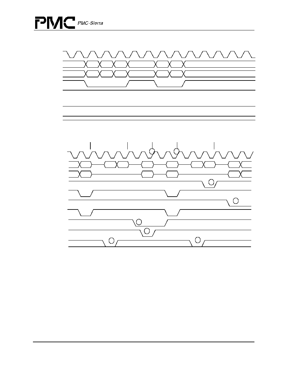
Proprietary and Confidential to PMC-Sierra, Inc and for its Customer's Internal Use
31
Document ID: PMC-2002175, Issue 1
RM7000TM Microprocessor with On-Chip Secondary Cache Datasheet
Released
Figure 10 Processor Block Write
Figure 11 Multiple Outstanding Reads
4.30 Data Prefetch
The RM7000 is the first PMC-Sierra design to support the MIPS IV integer data prefetch (
PREF
)
and floating-point data prefetch (
PREFX
) instructions. These instructions are used by the
compiler or by an assembly language programmer when it is known or suspected that an upcoming
data reference is going to miss in the cache. By appropriately placing a prefetch instruction, the
memory latency can be hidden under the execution of other instructions. If the execution of a
prefetch instruction would cause a memory management or address error exception the prefetch is
treated as a
NOP
.
SysClock
SysAD
Addr
Data0
Data1
Data2
Data3
SysCmd
ValidOut*
ValidIn*
RdRdy*
WrRdy*
Release*
Write
NData
NData
NData
NEOD
PRqst*
PAck*
Release*
TcMatch
SysClock
SysAD
SysCmd
ValidOut*
ValidIn*
Addr
1
Data1
Data1
Read
1
Data0
Addr
2
Data0
Data0
2
Read
2
NData
Master
Processor
Tertiary(Miss)
Tertiary(Miss)
Processor
Data1
2
NData
System
System
RspSwap*
1
2
3
4
5
6
7
8

Proprietary and Confidential to PMC-Sierra, Inc and for its Customer's Internal Use
32
Document ID: PMC-2002175, Issue 1
RM7000TM Microprocessor with On-Chip Secondary Cache Datasheet
Released
The "Hint" field of the data prefetch instruction is used to specify the action taken by the
instruction. The instruction can operate normally (that is, fetching data as if for a load operation) or
it can allocate and fill a cache line with zeroes on a primary data cache miss.
4.31 Enhanced Write Modes
Like previous MIPS processor designs, the RM7000 implements two enhancements to the original
R4000 write mechanism: Write Reissue and Pipeline Writes. In write reissue mode, a write rate of
one write every two bus cycles can be achieved. A write issues if WrRdy* is asserted two cycles
earlier and is still asserted during the issue cycle. If it is not still asserted then the last write will
reissue. Pipelined writes have the same two bus cycle write repeat rate, but can issue one
additional write following the deassertion of WrRdy*.
4.32 External Requests
The RM7000 can respond to certain requests issued by an external device. These requests take one
of two forms: Write requests and Null requests. An external device executes a write request when it
wishes to update one of the processors writable resources such as the internal interrupt register. A
null request is executed when the external device wishes the processor to reassert ownership of the
processor external interface. Typically a null request will be executed after an external device, that
has acquired control of the processor interface via ExtRqst*, has completed an independent
transaction between itself and system memory in a system where memory is connected directly to
the SysAD bus. Normally this transaction would be a DMA read or write from the I/O system.
4.33 Test/Breakpoint Registers
To increase both observability and controllability of the processor thereby easing hardware and
software debugging, a pair of Test/Break-point, or Watch, registers, Watch1 and Watch2, have
been added to the RM7000. Each Watch register can be separately enabled to watch for a load
address, a store address, or an instruction address. All address comparisons are done on physical
addresses. An associated register, Watch Mask, has also been added so that either or both of the
Watch registers can compare against an address range rather than a specific address. The range
granularity is limited to a power of two.
When enabled, a match of either Watch register results in an exception. If the Watch is enabled for
a load or store address then the exception is the Watch exception as defined for the R4000 with
Cause exception code twenty-three. If the Watch is enabled for instruction addresses then a newly
defined Instruction Watch exception is taken and the Cause code is sixteen. The Watch register
which caused the exception is indicated by Cause bits 25..24. Table 9 summarizes a Watch
operation.
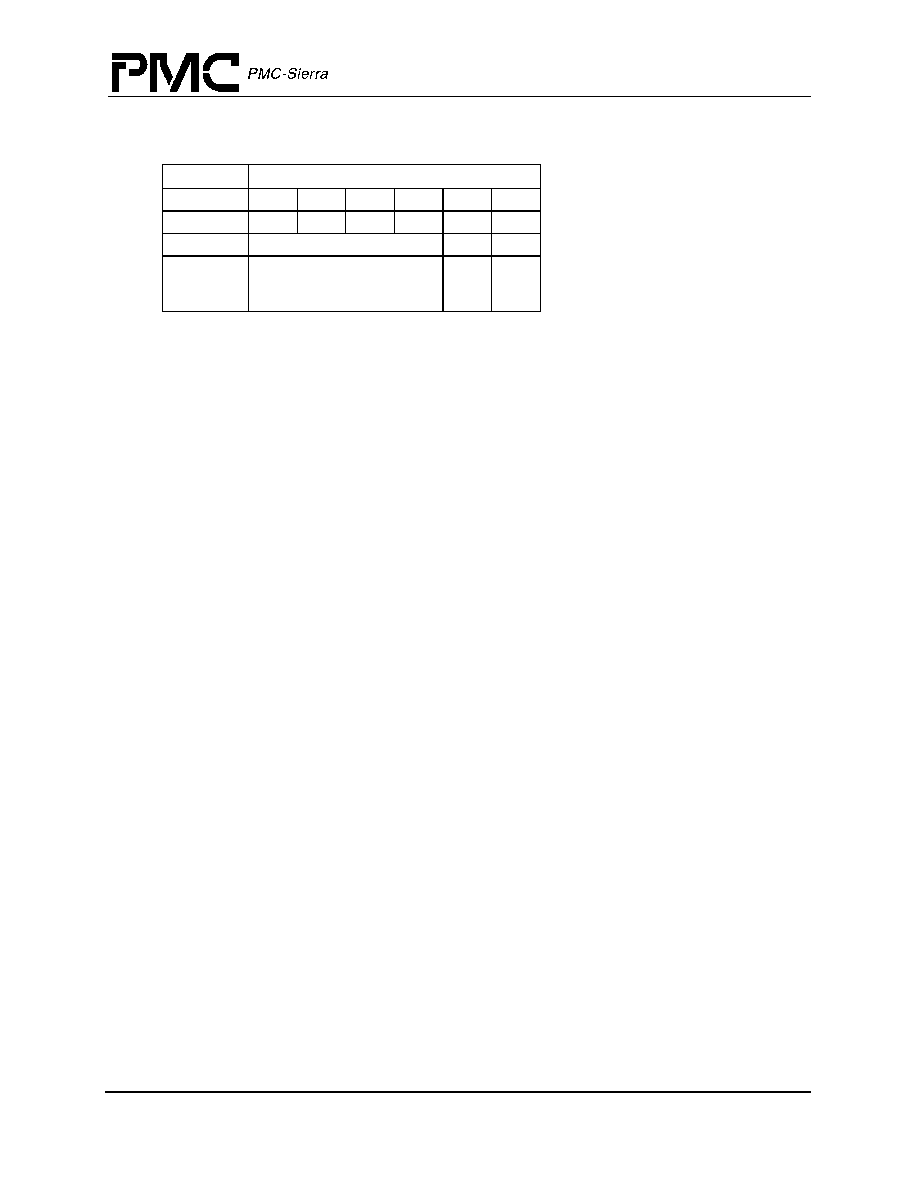
Proprietary and Confidential to PMC-Sierra, Inc and for its Customer's Internal Use
33
Document ID: PMC-2002175, Issue 1
RM7000TM Microprocessor with On-Chip Secondary Cache Datasheet
Released
Table 9 Watch Control Register
4.34 Performance Counters
Like the Test/Break-point capability described above, the Performance Counter feature has been
added to improve the observability and controllability of the processor thereby easing system
debug and, especially in the case of the performance counters, easing system tuning.
The Performance Counter feature is implemented using two new CP0 registers, PerfCount and
PerfControl. The PerfCount register is a 32-bit writable counter which causes an interrupt when bit
31 is set. The PerfControl register is a 32-bit register containing a five bit field which selects one
of twenty-two event types as well as a handful of bits which control the overall counting function.
Note that only one event type can be counted at a time and that counting can occur for user code,
kernel code, or both. The event types and control bits are listed in Table 10.
Register
Bit Field/Function
63
62
61
60:36
35:2
1:0
Watch1, 2
Store
Load
Instr
0
Addr
0
31:2
1
0
Watch Mask
Mask
Mask
Watch
2
Mask
Watch
1

Proprietary and Confidential to PMC-Sierra, Inc and for its Customer's Internal Use
34
Document ID: PMC-2002175, Issue 1
RM7000TM Microprocessor with On-Chip Secondary Cache Datasheet
Released
Table 10 Performance Counter Control
The performance counter interrupt will only occur when interrupts are enabled in the Status
register, IE=1, and Interrupt Mask bit 13 (IM[13]) of the coprocessor 0 interrupt control register is
not set.
PerfControl
Field
Description
4..0
Event Type
00:
Clock cycles
01:
Total instructions issued
02:
Floating-point instructions issued
03:
Integer instructions issued
04:
Load instructions issued
05:
Store instructions issued
06:
Dual issued pairs
07:
Branch prefetches
08:
External Cache Misses
09:
Stall cycles
0A:
Secondary cache misses
0B:
Instruction cache misses
0C:
Data cache misses
0D:
Data TLB misses
0E:
Instruction TLB misses
0F:
Joint TLB instruction misses
10:
Joint TLB data misses
11:
Branches taken
12:
Branches issued
13:
Secondary cache writebacks
14:
Primary cache writebacks
15:
Dcache miss stall cycles (cycles where both cache miss tokens taken and a third
address is requested)
16:
Cache misses
17:
FP possible exception cycles
18:
Slip Cycles due to multiplier busy
19:
Coprocessor 0 slip cycles
1A:
Slip cycles doe to pending non-blocking loads
1B:
Write buffer full stall cycles
1C:
Cache instruction stall cycles
1D:
Multiplier stall cycles
1E:
Stall cycles due to pending non-blocking loads - stall start of exception
7..5
Reserved (must be zero)
8
Count in Kernel Mode
0:
Disable
1:
Enable
9
Count in User Mode
0:
Disable
1:
Enable
10
Count Enable
0:
Disable
1:
Enable
31..11
Reserved (must be zero)

Proprietary and Confidential to PMC-Sierra, Inc and for its Customer's Internal Use
35
Document ID: PMC-2002175, Issue 1
RM7000TM Microprocessor with On-Chip Secondary Cache Datasheet
Released
Since the performance counter can be set up to count clock cycles, it can be used as either a) a
second timer or b) a watchdog interrupt. A watchdog interrupt can be used as an aid in debugging
system or software "hangs." Typically the software is setup to periodically update the count so that
no interrupt will occur. When a hang occurs the interrupt ultimately triggers thereby breaking free
from the hang-up.
4.35 Interrupt Handling
In order to provide better real time interrupt handling, the RM7000 provides an extended set of
hardware interrupts each of which can be separately prioritized and separately vectored.
In addition to the six external interrupt pins available on the R4000 and R5000 family processors,
the RM7000 provides four more interrupt pins for a total of ten external interrupts.
As described above, the performance counter is also a hardware interrupt source, INT[13]. Also,
whereas the R4000 and R5000 family processors map the timer interrupt onto INT[7], the
RM7000 provides a separate interrupt, INT[12], for this purpose freeing INT[7] for use as a pure
external interrupt.
All of these interrupts, INT[13..0], the Performance Counter, and the Timer, have corresponding
interrupt mask bits, IM[13..0], and interrupt pending bits, IP[13..0], in the Status, Interrupt
Control, and Cause registers. The bit assignments for the Interrupt Control and Cause registers are
shown in Table 11 and Table 12. The Status register has not changed from the RM5200 Family and
R5000, and is not shown.
The IV bit in the Cause register is the global enable bit for the enhanced interrupt features. If this
bit is clear then interrupt operation is compatible with the RM5200 Family and R5000. Although
not related to the interrupt mechanism, note that the W1 and W2 bits indicate which Watch register
caused a particular Watch exception.
In the Interrupt Control register, the interrupt vector spacing is controlled by the Spacing field as
described below. The Interrupt Mask field (IM[15..8]) contains the interrupt mask for interrupts
eight through thirteen. IM[15..14] are reserved for future use. The Timer Exclusive (TE) bit if set
moves the Timer interrupt to INT[12]. If clear, the Timer interrupt will be or'ed into INT[7] as on
the R5000.
The Interrupt Control register uses IM13 to enable the Performance Counter Control.
Priority of the interrupts is set via two new coprocessor 0 registers called Interrupt Priority Level
Lo (IPLLO) and Interrupt Priority Level Hi (IPLHI).

Proprietary and Confidential to PMC-Sierra, Inc and for its Customer's Internal Use
36
Document ID: PMC-2002175, Issue 1
RM7000TM Microprocessor with On-Chip Secondary Cache Datasheet
Released
Table 11 Cause Register
Table 12 Interrupt Control Register
Table 13 IPLLO Register
Table 14 IPLHI Register
These two registers contain a four-bit field corresponding to each interrupt thereby allowing each
interrupt to be programmed with a priority level from 0 to 13 inclusive. The priorities can be set in
any manner including having all the priorities set exactly the same. Priority 0 is the highest level
and priority 15 the lowest. The format of the priority level registers is shown in Table 13 and Table
14 above. The priority level registers are located in the coprocessor 0 control register space. For
further details about the control space see the section describing coprocessor 0.
In addition to programmable priority levels, the RM7000 also permits the spacing between
interrupt vectors to be programmed. For example, the minimum spacing between two adjacent
vectors is 0x20 while the maximum is 0x200. This programmability allows the user to either set up
the vectors as jumps to the actual interrupt routines or, if interrupt latency is paramount, to include
the entire interrupt routine at the vector. Table 15 illustrates the complete set of vector spacing
selections along with the coding as required in the Interrupt Control register bits 4:0.
In general, the active interrupt priority combined with the spacing setting generates a vector offset
which is then added to the interrupt base address of 0x200 to generate the interrupt exception
offset. This offset is then added to the exception base to produce the final interrupt vector address.
31
30
29,28
27
26
25
24
23..8
7
6..2
0,1
BD
0
CE
0
W2
W1
IV
IP[15..0]
0
EXC
0
31..16
15..8
7
6..5
4..0
0
IM[15..8] TE
0
Spacing
31..28
27..24
23..20
19..16
15..12
11..8
7..4
3..0
IPL7
IPL6
IPL5
IPL4
IPL3
IPL2
IPL1
IPL0
31..28
27..24
23..20
19..16
15..12
11..8
7..4
3..0
0
0
IPL13
IPL12
IPL11
IPL10
IPL9
IPL8

Proprietary and Confidential to PMC-Sierra, Inc and for its Customer's Internal Use
37
Document ID: PMC-2002175, Issue 1
RM7000TM Microprocessor with On-Chip Secondary Cache Datasheet
Released
Table 15 Interrupt Vector Spacing
4.36 Standby Mode
The RM7000 provides a means to reduce the amount of power consumed by the internal core
when the CPU would not otherwise be performing any useful operations. This state is known as
Standby Mode.
Executing the
WAIT
instruction enables interrupts and enters Standby Mode. When the
WAIT
instruction completes the W pipe stage, if the SysAD bus is currently idle, the internal processor
clocks will stop thereby freezing the pipeline. The phase lock loop, or PLL, internal timer/counter,
and the "wake up" input pins: INT[9:0]*, NMI*, ExtReq*, Reset*, and ColdReset* continue to
operate in their normal fashion. If the SysAD bus is not idle when the WAIT instruction completes
the W pipe stage, then the
WAIT
is treated as a
NOP
. Once the processor is in Standby, any
interrupt, including the internally generated timer interrupt, will cause the processor to exit
Standby and resume operation where it left off. The
WAIT
instruction is typically inserted in the
idle loop of the operating system or real time executive.
4.37 JTAG Interface
The RM7000 interface supports JTAG boundary scan in conformance with IEEE 1149.1. The
JTAG interface is especially helpful for checking the integrity of the processor's pin connections.
4.38 Boot-Time Options
Fundamental operational modes for the processor are initialized by the boot-time mode control
interface. The boot-time mode control interface is a serial interface operating at a very low
frequency (SysClock divided by 256). The low frequency operation allows the initialization
information to be kept in a low cost EPROM; alternatively the twenty or so bits could be generated
by the system interface ASIC.
Immediately after the VccOK signal is asserted, the processor reads a serial bit stream of 256 bits
to initialize all the fundamental operational modes. ModeClock runs continuously from the
assertion of VccOK.
4.39 Boot-Time Modes
The boot-time serial mode stream is defined in Table 16. Bit 0 is the bit presented to the processor
when
VccOK
is de-asserted; bit 255 is the last.
ICR[4..0] Spacing
0x0
0x000
0x1
0x020
0x2
0x040
0x4
0x080
0x8
0x100
0x10
0x200
others
reserved

Proprietary and Confidential to PMC-Sierra, Inc and for its Customer's Internal Use
38
Document ID: PMC-2002175, Issue 1
RM7000TM Microprocessor with On-Chip Secondary Cache Datasheet
Released
Table 16 Boot Time Mode Stream
Mode bit
Description
Mode bit
Description
0
reserved (must be zero)
17..16
System configuration identifiers - software visible
in processor Config[21..20] register
4..1
Write-back data rate
0:
DDDD
1:
DDxDDx
2:
DDxxDDxx
3:
DxDxDxDx
4:
DDxxxDDxxx
5:
DDxxxxDDxxxx
6:
DxxDxxDxxDxx
7:
DDxxxxxxDDxxxxxx
8:
DxxxDxxxDxxxDxxx
9-15: reserved
19..18
Reserved: Must be zero
7..5
SysClock to Pclock Multiplier
Mode bit 20 = 0 / Mode bit 20 = 1
0:
Multiply by 2/x
1:
Multiply by 3/x
2:
Multiply by 4/x
3:
Multiply by 5/2.5
4:
Multiply by 6/x
5:
Multiply by 7/3.5
6:
Multiply by 8/x
7:
Multiply by 9/4.5
20
Pclock to SysClock multipliers.
0:
Integer multipliers (2,3,4,5,6,7,8,9)
1:
Half integer multipliers (2.5,3.5,4.5)
8
Specifies byte ordering. Logically ORed with
BigEndian input signal.
0:
Little endian
1:
Big endian
23..21
Reserved: Must be zero
10..9
Non-Block Write Control
00:
R4000 compatible non-block writes
01:
reserved
10:
pipelined non-block writes
11:
non-block write re-issue
24
JTLB Size.
0: 48 dual-entry
1: 64 dual-entry
11
Timer Interrupt Enable/Disable
0:
Enable the timer interrupt on IP[5]
1:
Disable the timer interrupt on IP[5]
25
On-chip secondary cache control.
0:
Disable
1:
Enable
12
Enable the external tertiary cache
0:
Disable
1:
Enable
26
Enable two outstanding reads with out-of-order
return
0:
Disable
1:
Enable
14..13
Output driver strength - 100% = fastest
00:
67% strength
01:
50% strength
10:
100% strength
11:
83% strength
255..27
Reserved: Must be zero
15
External Tertiary cache RAM type:
0:
Dual-cycle deselect (DCD)
1:
Single-cycle deselect (SCD)
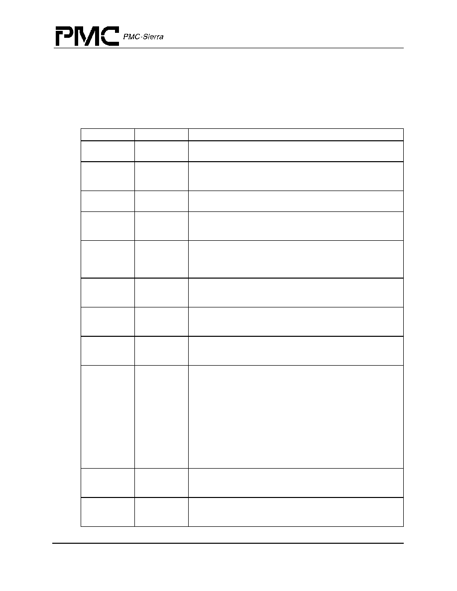
Proprietary and Confidential to PMC-Sierra, Inc and for its Customer's Internal Use
39
Document ID: PMC-2002175, Issue 1
RM7000TM Microprocessor with On-Chip Secondary Cache Datasheet
Released
5
Pin Descriptions
The following is a list of control, data, clock, tertiary cache, interrupt, and miscellaneous pins of
the RM7000.
Table 17
System interface Pins
Pin Name
Type
Description
ExtRqst*
Input
External request
Signals that the system interface is submitting an external request.
Release*
Output
Release interface
Signals that the processor is releasing the system interface to slave
state
RdRdy*
Input
Read Ready
Signals that an external agent can now accept a processor read.
WrRdy*
Input
Write Ready
Signals that an external agent can now accept a processor write
request.
ValidIn*
Input
Valid Input
Signals that an external agent is now driving a valid address or data on
the SysAD bus and a valid command or data identifier on the SysCmd
bus.
ValidOut*
Output
Valid output
Signals that the processor is now driving a valid address or data on the
SysAD bus and a valid command or data identifier on the SysCmd bus.
PRqst*
Output
Processor Request
When asserted this signal requests that control of the system interface
be returned to the processor. This is enabled by Mode Bit 26.
PAck*
Input
Processor Acknowledge
When asserted, in response to PRqst*, this signal indicates to the
processor that it has been granted control of the system interface.
RspSwap*
Input
Response Swap
RspSwap* is used by the external agent to signal the processor when it
is about to return a memory reference out of order; i.e., of two
outstanding memory references, the data for the second reference is
being returned ahead of the data for the first reference. In order that the
processor will have time to switch the address to the tertiary cache, this
signal must be asserted a minimum of two cycles prior to the data itself
being presented. Note that this signal works as a toggle; i.e., for each
cycle that it is held asserted the order of return is reversed. By default,
anytime the processor issues a second read it is assumed that the
reads will be returned in order; i.e., no action is required if the reads are
indeed returned in order. This is enabled by Mode Bit 26.
RdType
Output
Read Type
During the address cycle of a read request, RdType indicates whether
the read request is an instruction read or a data read.
SysAD(63:0)
Input/Output
System address/data bus
A 64-bit address and data bus for communication between the
processor and an external agent.

Proprietary and Confidential to PMC-Sierra, Inc and for its Customer's Internal Use
40
Document ID: PMC-2002175, Issue 1
RM7000TM Microprocessor with On-Chip Secondary Cache Datasheet
Released
Table 18
Clock/control interface Pins
SysADC(7:0)
Input/Output
System address/data check bus
An 8-bit bus containing parity check bits for the SysAD bus during data
cycles.
SysCmd(8:0)
Input/Output
System command/data identifier bus
A 9-bit bus for command and data identifier transmission between the
processor and an external agent.
SysCmdP
Input/Output
System Command/Data Identifier Bus Parity
For the RM7000, unused on input and zero on output.
Pin Name
Type
Description
SysClock
Input
System clock
Master clock input used as the system interface reference clock. All
output timings are relative to this input clock. Pipeline operation
frequency is derived by multiplying this clock up by the factor selected
during boot initialization
VccP
Input
Vcc for PLL
Quiet VccInt for the internal phase locked loop. Must be connected to
VccInt through a filter circuit.
VssP
Input
Vss for PLL
Quiet Vss for the internal phase locked loop. Must be connected to
VssInt through a filter circuit.
Pin Name
Type
Description
Proprietary and Confidential to PMC-Sierra, Inc and for its Customer's Internal Use
41
Document ID: PMC-2002175, Issue 1
RM7000TM Microprocessor with On-Chip Secondary Cache Datasheet
Released
Table 19
Tertiary cache interfacePins
Pin Name
Type
Description
TcCLR*
Output
Tertiary Cache Block Clear
Requests that all valid bits be cleared in the Tag RAMs. Many RAM's
may not support a block clear therefore the block clear capability is not
required for the cache to operate.
TcCWE*(1:0)
Output
Tertiary Cache Write Enable
Asserted to cause a write to the cache. Two identical signals are
provided to balance the capacitive load relative to the remaining cache
interface signals.
TcDCE*(1:0)
Output
Tertiary Cache Data RAM Chip Enable
When asserted this signal causes the data RAM's to read out their
contents. Two identical signals are provided to balance the capacitive
load relative to the remaining cache interface signals
TcDOE*
Input
Tertiary Cache Data RAM Output Enable
When asserted this signal causes the data RAM's to drive data onto
their I/O pins. This signal is monitored by the processor to determine
when to drive the data RAM write enable in a tertiary cache miss refill
sequence.
TcLine(17:0)
Output
Tertiary Cache Line Index
TcMatch
Input
Tertiary Cache Tag Match
This signal is asserted by the cache Tag RAM's when a match occurs
between the value on its data inputs and the contents of the addressed
location in the RAM.
TcTCE*
Output
Tertiary Cache Tag RAM Chip Enable
When asserted this signal will cause either a probe or a write of the Tag
RAM's depending on the state of the Tag RAM's write enable signal.
This signal is monitored by the external agent and indicates to it that a
tertiary cache access is occurring.
TcTDE*
Output
Tertiary Cache Tag RAM Data Enable
When asserted this signal causes the value on the data inputs of the
Tag RAM to be latched into the RAM. If a refill of the RAM is necessary,
this latched value will be written into the Tag RAM array. Latching the
Tag allows a shared address/data bus to be used without incurring a
penalty to re-present the Tag during the refill sequence.
TcTOE*
Output
Tertiary Cache Tag RAM Output Enable
When asserted this signal causes the Tag RAM's to drive data onto
their I/O pins.
TcWord(1:0)
Input/Output
Tertiary Cache Double Word Index
Driven by the processor on cache hits and by the external agent on
cache miss refills.
TcValid
Input/Output
Tertiary Cache Valid
This signal is driven by the processor as appropriate to make a cache
line valid or invalid. On Tag read operations the Tag RAM will drive this
signal to indicate the line state.
Proprietary and Confidential to PMC-Sierra, Inc and for its Customer's Internal Use
42
Document ID: PMC-2002175, Issue 1
RM7000TM Microprocessor with On-Chip Secondary Cache Datasheet
Released
Table 20
Interrupt Interface Pins
Table 21
JTAG Interface Pins
Table 22
Initialization Interface Pins
Pin Name
Type
Description
Int*(9:0)
Input
Interrupt
Ten general processor interrupts, bit-wise ORed with bits 9:0 of the
interrupt register.
NMI*
Input
Non-maskable interrupt
Non-maskable interrupt, ORed with bit 15 of the interrupt register (bit 6
in R5000 compatibility mode).
Pin Name
Type
Description
JTDI
Input
JTAG data in
JTAG serial data in.
JTCK
Input
JTAG clock input
JTAG serial clock input.
JTDO
Output
JTAG data out
JTAG serial data out.
JTMS
Input
JTAG command
JTAG command signal, signals that the incoming serial data is
command data.
Pin Name
Type
Description
BigEndian
Input
Big Endian / Little Endian Control
Allows the system to change the processor addressing mode without
rewriting the mode ROM.
VccOK
Input
Vcc is OK
When asserted, this signal indicates to the RM7000 that the 2.5V
power supply has been above 2.25V for more than 100 milliseconds
and will remain stable. The assertion of VccOK initiates the reading of
the boot-time mode control serial stream.
ColdReset*
Input
Cold Reset
This signal must be asserted for a power on reset or a cold reset.
ColdReset must be de-asserted synchronously with SysClock.
Reset*
Input
Reset
This signal must be asserted for any reset sequence. It may be
asserted synchronously or asynchronously for a cold reset, or
synchronously to initiate a warm reset. Reset must be de-asserted
synchronously with SysClock.
ModeClock
Output
Boot Mode Clock
Serial boot-mode data clock output at the system clock frequency
divided by two hundred and fifty six.
ModeIn
Input
Boot Mode Data In
Serial boot-mode data input.

Proprietary and Confidential to PMC-Sierra, Inc and for its Customer's Internal Use
43
Document ID: PMC-2002175, Issue 1
RM7000TM Microprocessor with On-Chip Secondary Cache Datasheet
Released
6
Absolute Maximum Ratings
1
Symbol
Rating
Limits
Unit
V
TERM
Terminal Voltage with respect to VSS
≠0.5
2
to +3.9
V
T
CASE
Operating Temperature
0 to +85
∞
C
T
STG
Storage Temperature
≠55 to +125
∞
C
I
IN
DC Input Current
3
±20
mA
I
OUT
DC Output Current
4
±20
mA
Notes
1. Stresses greater than those listed under ABSOLUTE MAXIMUM RATINGS may cause per-
manent damage to the device. This is a stress rating only and functional operation of the
device at these or any other conditions above those indicated in the operational sections of
this specification is not implied. Exposure to absolute maximum rating conditions for
extended periods may affect reliability.
2. V
IN
minimum = -2.0 V for pulse width less than 15 ns. V
IN
should not exceed 3.9 Volts.
3. When V
IN
< 0V or V
IN
> VccIO
4. Not more than one output should be shorted at a time. Duration of the short should not
exceed 30 seconds.
Proprietary and Confidential to PMC-Sierra, Inc and for its Customer's Internal Use
44
Document ID: PMC-2002175, Issue 1
RM7000TM Microprocessor with On-Chip Secondary Cache Datasheet
Released
7
Recommended Operating Conditions
Notes
1. VCC I/O should not exceed VccInt by greater than 1.2 V during the power-up sequence.
2. Applying a logic high state to any I/O pin before VccInt becomes stable is not recommended.
3. As specified in IEEE 1149.1 (JTAG), the JTMS pin must be held high during reset to avoid
entering JTAG test mode. Refer to the RM7000 Family Users Manual, Appendix E.
4. VccP must be connected to VccInt through a passive filter circuit. See RM7000 Family User's
Manual for recommended circuit.
CPU Speed
Temperature
Vss
VccInt
VccIO
VccP
200 - 250 MHz
0
∞
C to +85
∞
C
(Case)
0V
2.5V
±
5%
3.3V
±
5%
2.5V
±
5%
266 MHz
0
∞
C to +85
∞
C
(Case)
0V
2.5V
±
3%
3.3V
±
5%
2.5V
±
3%
300 MHz
0
∞
C to +70
∞
C
(Case)
0V
2.6V
±
.05V
3.3V
±
5%
2.6V
±
.05V

Proprietary and Confidential to PMC-Sierra, Inc and for its Customer's Internal Use
45
Document ID: PMC-2002175, Issue 1
RM7000TM Microprocessor with On-Chip Secondary Cache Datasheet
Released
8
DC Electrical Characteristics
Parameter
Minimum
Maximum
Conditions
V
OL
0.2V
|I
OUT
|= 100
µ
A
V
OH
VccIO - 0.2V
V
OL
0.4V
|I
OUT
| = 2 mA
V
OH
2.4V
V
IL
-0.3V
0.8V
V
IH
2.0V
VccIO + 0.3V
I
IN
±1
5
µ
A
±1
5
µ
A
V
IN
=
0
V
IN
= VccIO
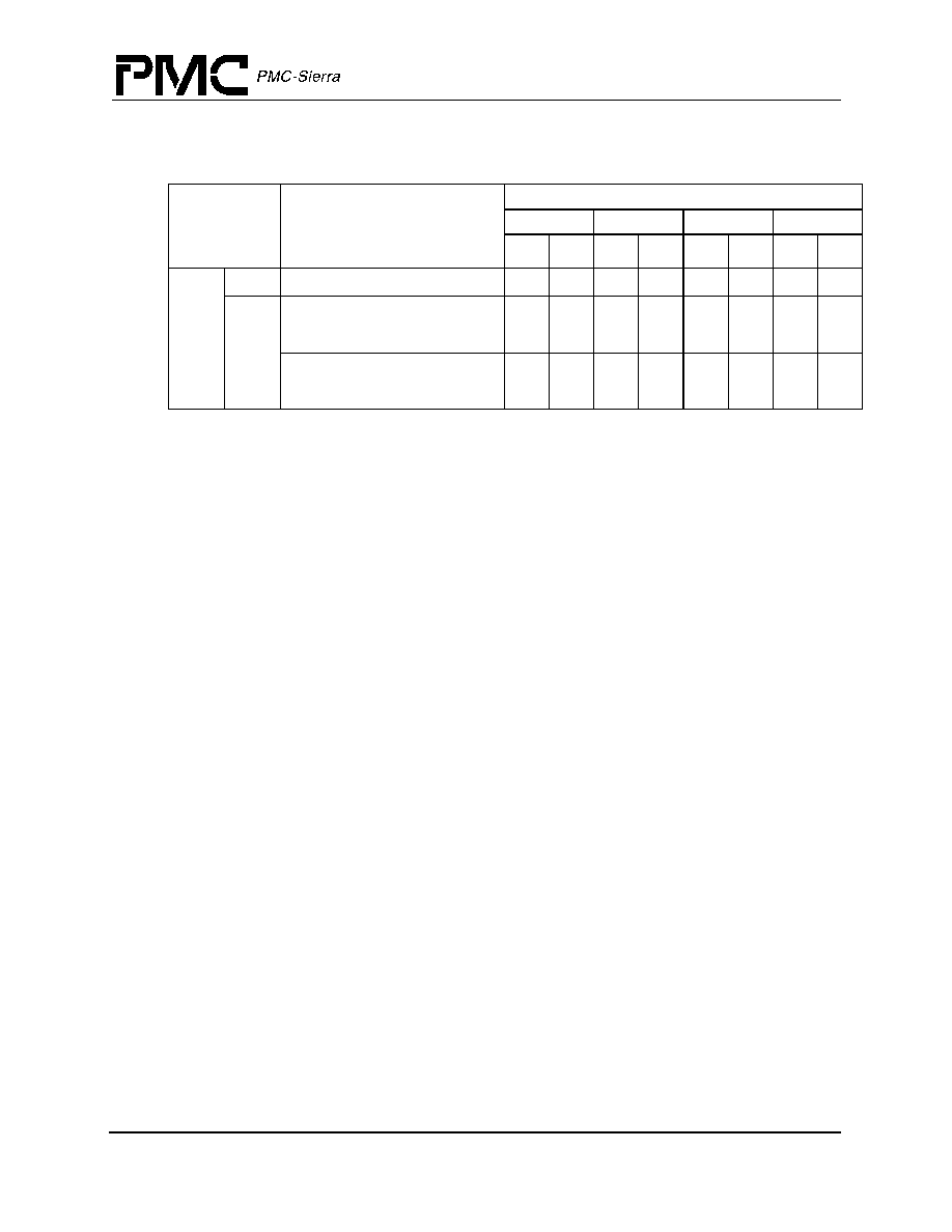
Proprietary and Confidential to PMC-Sierra, Inc and for its Customer's Internal Use
46
Document ID: PMC-2002175, Issue 1
RM7000TM Microprocessor with On-Chip Secondary Cache Datasheet
Released
9
Power Consumption
Notes
1. Typical integer instruction mix and cache miss rates with worst case supply voltage.
2. Worst case instruction mix with worst case supply voltage.
3. I/O supply power is application dependant, but typically <10% of VccInt.
Parameter
Conditions
CPU Clock Speed
200 MHz
250 MHz
266 MHz
300 MHz
Typ
1
Max
Typ
1
Max
Typ
1
Max
Typ
1
Max
VccInt
Power
(mWatt
s)
standb
No SysAD bus activity
500
1000
1500
2000
active
R4000 write protocol with no FPU
operation (integer instructions
only)
2200
4400
2700
5400
2800
5600
3800
7600
Write re-issue or pipelined writes
with superscalar (Integer and
floating point instructions)
2550
5100
3150
6300
3300
6600
4250
8500
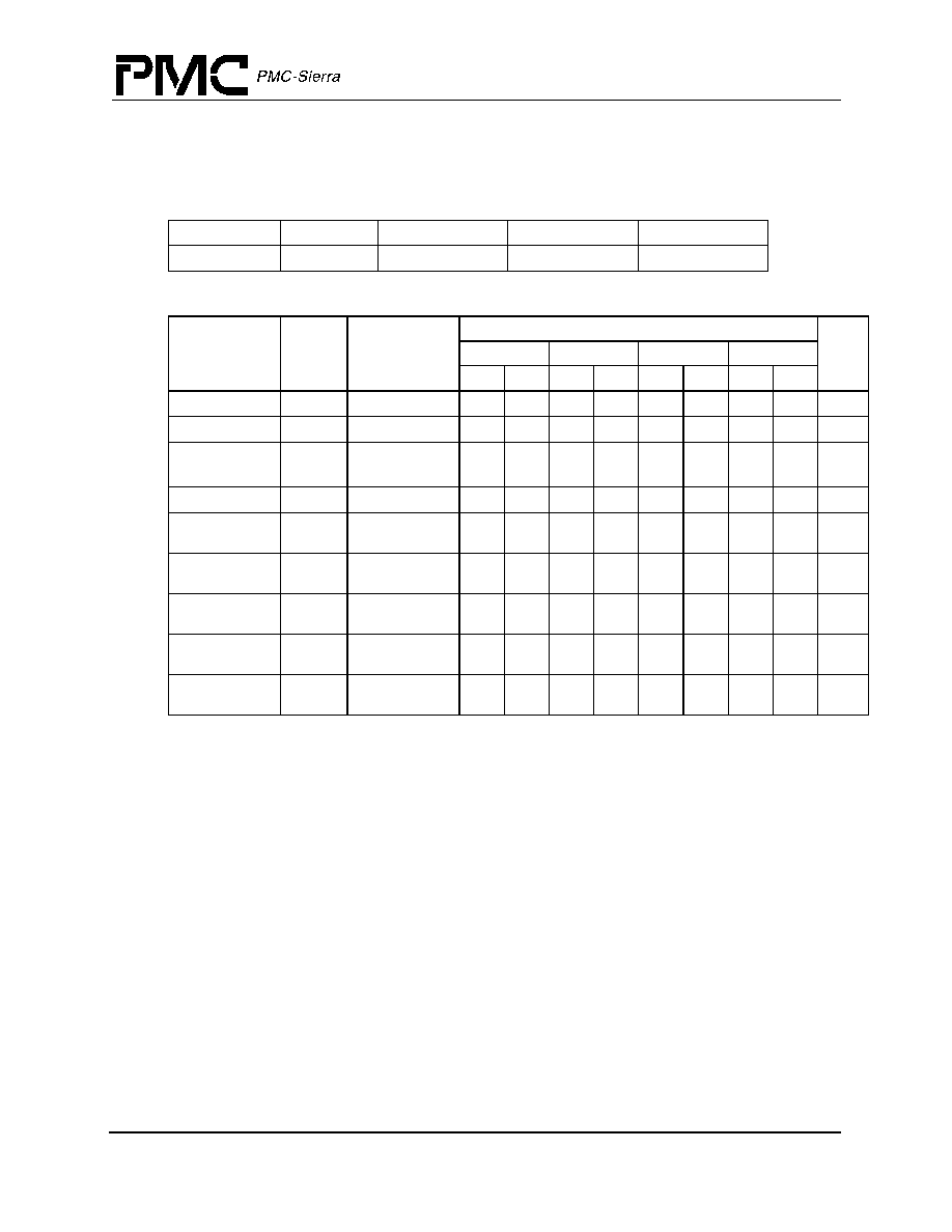
Proprietary and Confidential to PMC-Sierra, Inc and for its Customer's Internal Use
47
Document ID: PMC-2002175, Issue 1
RM7000TM Microprocessor with On-Chip Secondary Cache Datasheet
Released
10
AC Electrical Characteristics
10.1 Capacitive Load Deration
10.2 Clock Parameters
Parameter
Symbol
Min
Max
Units
Load Derate
C
LD
2
ns/25pF
Parameter
Symbol
Test
Conditions
CPU Speed
Units
200 MHz
250 MHz
266 MHz
300 MHz
Min
Max
Min
Max
Min
Max
Min
Max
SysClock High
t
SCHigh
Transition
5ns
3
3
3
3
ns
SysClock Low
t
SCLow
Transition
5ns
3
3
3
3
ns
SysClock
Frequency
7
25
100
25
125
33.3
105
33.3
120
MHz
SysClock Period t
SCP
40
40
30
30
ns
Clock Jitter for
SysClock
t
JitterIn
±
200
±
150
±
150
±
150
ps
SysClock Rise
Time
t
SCRise
2
2
2
2
ns
SysClock Fall
Time
t
SCFall
2
2
2
2
ns
ModeClock
Period
t
ModeCKP
256
256
256
256
t
SCP
JTAG Clock
Period
t
JTAGCKP
4
4
4
4
t
SCP
Note:
Operation of the RM7000 is only guaranteed with the Phase Lock Loop Enabled.
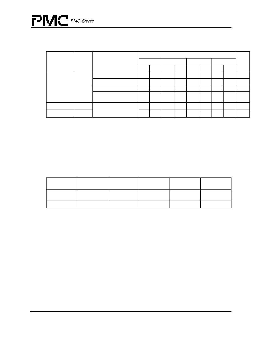
Proprietary and Confidential to PMC-Sierra, Inc and for its Customer's Internal Use
48
Document ID: PMC-2002175, Issue 1
RM7000TM Microprocessor with On-Chip Secondary Cache Datasheet
Released
10.3 System Interface Parameters
10.4 Boot-Time Interface Parameters
Parameter
1
Symbol Test Conditions
CPU Speed
Units
200 MHz
250 MHz
266 MHz
300 MHz
Min Max
Min
Max
Min
Max
Min
Max
Data Output
2,3
t
DO
mode14..13 = 10 (fastest) 1.0
5.0
1.0
5.0
1.0
4.5
1.0
4.5
ns
mode14..13 = 11
1.0
5.5
1.0
5.5
1.0
5.0
1.0
4.5
ns
mode14..13 = 00
1.0
6.0
1.0
6.0
1.0
5.0
1.0
5.0
ns
mode14..13 = 01
(slowest)
1.0
7.0
1.0
6.5
1.0
6.0
1.0
5.5
ns
Data Setup
4
t
DS
t
rise
= see above table
t
fall
= see above table
2.5
2.5
2.5
2.5
ns
Data Hold
4
t
DH
1.0
1.0
1.0
1.0
ns
Notes
1. Timings are measured from 0.425 x VccIO of clock to 0.425 x VccIO of signal for 3.3V I/O.
2. Capacitive load for all output timings is 50 pF.
3. Data Output timing applies to all signal pins whether tristate I/O or output only.
4. Setup and Hold parameters apply to all signal pins whether tristate I/O or input only.
5. Only mode 14:13 = 10 is tested and guaranteed.
Parameter
7
Symbol
Test Condi-
tions
Min
Max
Units
Mode Data
Setup
t
DS
4
SysClock cycles
Mode Data Hold t
DH
0
SysClock cycles

Proprietary and Confidential to PMC-Sierra, Inc and for its Customer's Internal Use
49
Document ID: PMC-2002175, Issue 1
RM7000TM Microprocessor with On-Chip Secondary Cache Datasheet
Released
11
Timing Diagrams
11.1 Clock Timing
Figure 12 Clock Timing
System Interface Timing (SysAD, SysCmd, ValidIn*, ValidOut*, etc.)
Figure 13 Input Timing
Figure 14 Output Timing
SysClock
t
Rise
t
Fall
t
High
t
Low
±t
JitterIn
t
DS
t
DH
Data
SysClock
Data
t
DOmin
t
DOmax
SysClock
Data
Data
Data
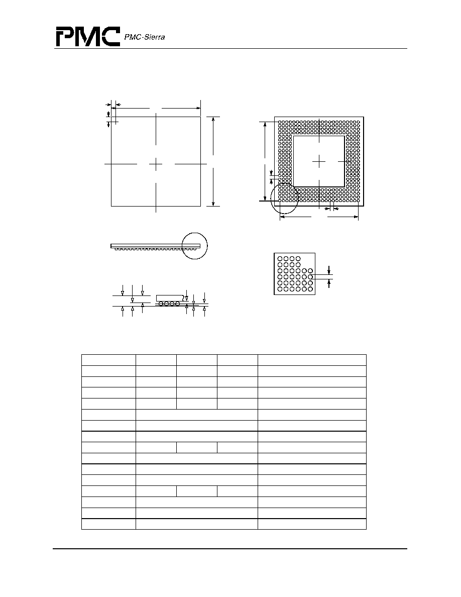
Proprietary and Confidential to PMC-Sierra, Inc and for its Customer's Internal Use
50
Document ID: PMC-2002175, Issue 1
RM7000TM Microprocessor with On-Chip Secondary Cache Datasheet
Released
12
Packaging Information
304 TBGA Drawing
Body Size: 31.0 x 31.0 mm Package
Symbol
Min
Nominal
Max
Note
A
1.45
1.55
1.65
Overall Thickness
A1
0.60
0.65
0.70
Ball Height
A2
0.85
0.90
0.95
Body Thickness
D, E
30.80
31.00
31.20
Body Size
D1, E1
27.94
Ball Footprint
M,N
23 x 23
Ball Matrix
M1
4
Number of Rows Deep
b
0.65
0.75
0.85
Ball Diameter
e
1.27
Ball Pitch
aaa
0.15
Coplanarity
bbb
0.15
Parallel
f
0.30
0.35
0.40
Seating Plan Clearance
P
0.25
Encapsulation Height
Theta JC
0.3
Deg. C/Watt
Theta JA
13
Deg. C/Watt @ 0 cfm air flow.
Note: All dimensions in millimeters unless otherwise indicated.
O
23 22 21 20 19 18 17 16 15 14 13 12 11 10 9 8 7 6 5 4 3 2 1
A
B
C
D
E
F
G
H
J
K
L
M
N
P
R
T
U
V
W
Y
AA
AB
AC
D1, M
D
E
TOP VIEW
BOTTOM VIEW
SIDE VIEW
O
A1 ball
corner
1.27 mm
1.27 mm
A
A1
A2
E1, N
e
e
DETAIL B
b
DETAIL B
DETAIL A
aaa
f
P
DETAIL A
ink mark

Proprietary and Confidential to PMC-Sierra, Inc and for its Customer's Internal Use
51
Document ID: PMC-2002175, Issue 1
RM7000TM Microprocessor with On-Chip Secondary Cache Datasheet
Released
13
RM7000 Pinout
Pin
Function
Pin
Function
Pin
Function
Pin
Function
A1
VccIO
A2
VssIO
A3
VssIO
A4
TcLine[11]
A5
Do not connect
A6
VsslO
A7
Do Not Connect A8
VsslO
A9
SysAD[32]
A10
SysADC[1]
A11
Do Not Connect A12
VsslO
A13
Vcclnt
A14
Vcclnt
A15
SysAD[63]
A16
VsslO
A17
SysAD[61]
A18
VsslO
A19
Do Not Connect A20
TcLine[4]
A21
VsslO
A22
VsslO
A23
VcclO
B1
Vsslnt
B2
VcclO
B3
Vsslnt
B4
VsslO
B5
TcLine[10]
B6
SysAD[35}
B7
SysAD[34]
B8
Vcclnt
B9
SysAD[33]
B10
SysADC[5]
B11
SysADC[0]
B12
Do Not Connect B13
SysADC[7]
B14
SysADC[6]
B15
Do Not Connect B16
SysAD[30]
B17
SysAD[29]
B18
SysAD[28]
B19
TcLine[5]
B20
VsslO
B21
Vsslnt
B22
VcclO
B23
VsslO
C1
VsslO
C2
Vsslnt
C3
VcclO
C4
VcclO
C5
Do Not Connect C6
TcLine[9]
C7
SysAD[3]
C8
SysAD[2]
C9
Vcclnt
C10
SysAD[0]
C11
SysADC[4]
C12
Vcclnt
C13
SysADC[3]
C14
SysADC[2]
C15
SysAD[62]
C16
Vcclnt
C17
SysAD[60]
C18
TcLine[6]
C19
Do Not Connect C20
VcclO
C21
VcclO
C22
Vsslnt
C23
VsslO
D1
TcLine[13]
D2
VsslO
D3
VcclO
D4
VcclO
D5
VcclO
D6
VcclO
D7
TcLine[8]
D8
Vcclnt
D9
VcclO
D10
SysAD[1]
D11
Vcclnt
D12
VcclO
D13
Vcclnt
D14
SysAD[31]
D15
VcclO
D16
Vcclnt
D17
TcLine[7]
D18
VcclO
D19
VcclO
D20
VcclO
D21
VcclO
D22
VsslO
D23
Do Not Connect
E1
Vcclnt
E2
TcLine[14]
E3
TcLine[12]
E4
VcclO
E20
VcclO
E21
Do Not Connect E22
Do Not Connect E23
TcLine[1]
F1
VsslO
F2
TcLine[16]
F3
TcLine[15]
F4
VcclO
F20
VcclO
F21
TcLine[3]
F22
TcLine[0]
F23
VsslO
G1
SysAD[36]
G2
SysAD[4]
G3
TcLine[17]
G4
Vcclnt
G20
TcLine[2]
G21
Vcclnt
G22
SysAD[59]
G23
SysAD[58]
H1
VsslO
H2
SysAD[37]
H3
SysAD[5]
H4
Do Not Connect
H20
Vcclnt
H21
SysAD[27]
H22
SysAD[26]
H23
VsslO
J1
SysAD[7]
J2
SysAD[6]
J3
Vcclnt
J4
VcclO
J20
VcclO
J21
Vccint
J22
SysAD[57]
J23
SysAD[56]
K1
SysAD[40]
K2
SysAD[8]
K3
SysAD[39]
K4
SysAD[38]
K20
SysAD[25]
K21
SysAD[24]
K22
SysAD[55]
K23
SysAD[23]
L1
SysAD[10]
L2
SysAD[41]
L3
SysAD[9]
L4
Vcclnt
L20
Vcclnt
L21
SysAD[54]
L22
SysAD[22]
L23
SysAD[53]
M1
VsslO
M2
SysAD[11]
M3
SysAD[42]
M4
VcclO

Proprietary and Confidential to PMC-Sierra, Inc and for its Customer's Internal Use
52
Document ID: PMC-2002175, Issue 1
RM7000TM Microprocessor with On-Chip Secondary Cache Datasheet
Released
M20
VcclO
M21
SysAD[52]
M22
SysAD[21]
M23
VsslO
N1
SysAD[43]
N2
Vcclnt
N3
SysAD[12]
N4
SysAD[44]
N20
SysAD[19]
N21
SysAD[51]
N22
Vcclnt
N23
SysAD[20]
P1
SysAD[13]
P2
SysAD[45]
P3
SysAD[14]
P4
Vcclnt
P20
Vcclnt
P21
SysAD[49]
P22
SysAD[18]
P23
SysAD[50]
R1
SysAD[46]
R2
SysAD[15]
R3
SysAD[47]
R4
VcclO
R20
VcclO
R21
SysAD[16]
R22
SysAD[48]
R23
SysAD[17]
T1
VsslO
T2
RspSwap*
T3
PRqst*
T4
Vcclnt
T20
ExtRqst*
T21
VccOK
T22
BigEndlan
T23
VsslO
U1
PAck*
U2
Vcclnt
U3
ModeClock
U4
JTCK
U20
Vcclnt
U21
NMI*
U22
Reset*
U23
ColdReset*
V1
VsslO
V2
JTDO
V3
JTMS
V4
VcclO
V20
VcclO
V21
INT[9]*
V22
Vcclnt
V23
VsslO
W1
JTDI
W2
VcclO
W3
Do Not Connect W4
VcclO
W20
VcclO
W21
INT[6]*
W22
INT[8]*
W23
Vcclnt
Y1
Do Not Connect Y2
VsslO
Y3
VcclO
Y4
VcclO
Y5
VcclO
Y6
VcclO
Y7
RdRdy*
Y8
Release*
Y9
VcclO
Y10
TcWord[0]
Y11
Vcclnt
Y12
VcclO
Y13
SysCmd[5]
Y14
Vcclnt
Y15
VcclO
Y16
Vcclnt
Y17
INT[2]*
Y18
VcclO
Y19
VcclO
Y20
VcclO
Y21
VcclO
Y22
VsslO
Y23
INT[7]*
AA1
VsslO
AA2
Vsslnt
AA3
VcclO
AA4
VcclO
AA5
Do Not Connect
AA6
TcMatch
AA7
ValidOut*
AA8
SysClock
AA9
Vcclnt
AA10 Do Not Connect AA11 Do Not Connect AA12 SysCmd[0]
AA13 SysCmd[4]
AA14 SysCmd[8]
AA15 TcTCE*
AA16 TcValid
AA17 Vcclnt
AA18 INT[3]*
AA19 Do Not Connect AA20 VcclO
AA21 VcclO
AA22 Vsslnt
AA23 VsslO
AB1
VsslO
AB2
VcclO
AB3
Vsslnt
AB4
VsslO
AB5
Modeln
AB6
Validin*
AB7
VccP
AB8
Vcclnt
AB9
Vcclnt
AB10 TcCWE[0]*
AB11 TcDCE[0]*
AB12 SysCmd[1]
AB13 SysCmd[3]
AB14 SysCmd[7]
AB15 TcClr*
AB16 TcTDE*
AB17 TcDOE*
AB18 INT[0]*
AB19 INT[4]*
AB20 VsslO
AB21 Vsslnt
AB22 VcclO
AB23 Vsslnt
AC1
VcclO
AC2
Vsslnt
AC3
VsslO
AC4
RdType
AC5
WrRdy*
AC6
VsslO
AC7
VssP
AC8
VsslO
AC9
TcWord[1]
AC10 TcCWE[1]*
AC11 TcDCE[1]*
AC12 VsslO
AC13 SysCmd[2]*
AC14 SysCmd[6]
AC15 SysCmdP
AC16 VsslO
AC17 TcTOE*
AC18 VsslO
AC19 INT[1]*
AC20 INT[5]*
AC21 VsslO
AC22 VsslO
AC23 VcclO
Pin
Function
Pin
Function
Pin
Function
Pin
Function
Proprietary and Confidential to PMC-Sierra, Inc and for its Customer's Internal Use
53
Document ID: PMC-2002175, Issue 1
RM7000TM Microprocessor with On-Chip Secondary Cache Datasheet
Released
14
Ordering Information
RM7000
-123
T
I
Temperature Grade:
(blank) = commercial
I = Industrial
Package Type:
Device Maximum Speed
Device Type
T = TBGA
S = SBGA
Valid Combinations
RM7000-200T
RM7000-250T
RM7000-266T
RM7000-300T
Legacy Devices
Recommended Conversions
RM7000-200S
RM7000-200T
RM7000-225S
RM7000-250T
RM7000-250S
RM7000-250T
RM7000-263S
RM7000-266T
RM7000-300S
RM7000-300T

Proprietary and Confidential to PMC-Sierra, Inc and for its Customer's Internal Use
54
Document ID: PMC-2002175, Issue 1
RM7000TM Microprocessor with On-Chip Secondary Cache Datasheet
Released