 | –≠–ª–µ–∫—Ç—Ä–æ–Ω–Ω—ã–π –∫–æ–º–ø–æ–Ω–µ–Ω—Ç: TIPL761C | –°–∫–∞—á–∞—Ç—å:  PDF PDF  ZIP ZIP |
TIPL761B, TIPL761C
NPN SILICON POWER TRANSISTORS
P R O D U C T I N F O R M A T I O N
1
MAY 1989 - REVISED MARCH 1997
Copyright © 1997, Power Innovations Limited, UK
Information is current as of publication date. Products conform to specifications in accordance
with the terms of Power Innovations standard warranty. Production processing does not
necessarily include testing of all parameters.
q
Rugged Triple-Diffused Planar Construction
q
4 A Continuous Collector Current
q
Operating Characteristics Fully Guaranteed
at 100∞C
q
1200 Volt Blocking Capability
q
100 W at 25∞C Case Temperature
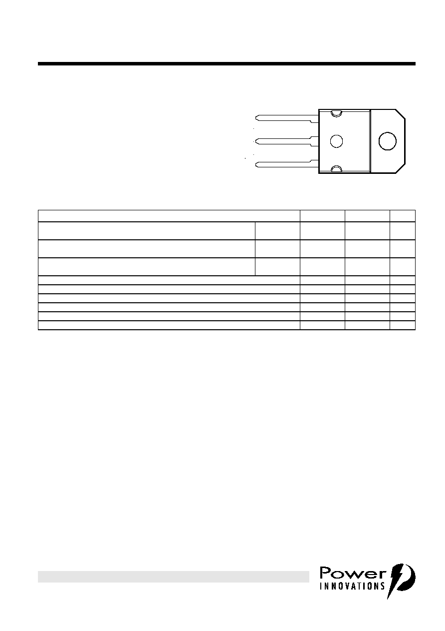
SOT-93 PACKAGE
(TOP VIEW)
Pin 2 is in electrical contact with the mounting base.
MDTRAA
B
C
E
1
2
3
absolute maximum ratings
at 25∞C case temperature (unless otherwise noted)
NOTE
1: This value applies for t
p
10 ms, duty cycle
2%.
RATING
SYMBOL
VALUE
UNIT
Collector-base voltage (I
E
= 0)
TIPL761B
TIPL761C
V
CBO
1100
1200
V
Collector-emitter voltage (V
BE
= 0)
TIPL761B
TIPL761C
V
CES
1100
1200
V
Collector-emitter voltage (I
B
= 0)
TIPL761B
TIPL761C
V
CEO
500
550
V
Emitter-base voltage
V
EBO
10
V
Continuous collector current
I
C
4
A
Peak collector current (see Note 1)
I
CM
8
A
Continuous device dissipation at (or below) 25∞C case temperature
P
tot
100
W
Operating junction temperature range
T
j
-65 to +150
∞C
Storage temperature range
T
stg
-65 to +150
∞C

TIPL761B, TIPL761C
NPN SILICON POWER TRANSISTORS
2
MAY 1989 - REVISED MARCH 1997
P R O D U C T I N F O R M A T I O N
NOTES: 2. Inductive loop switching measurement.
3. These parameters must be measured using pulse techniques, t
p
= 300 µs, duty cycle
2%.
4. These parameters must be measured using voltage-sensing contacts, separate from the current carrying contacts.
Voltage and current values shown are nominal; exact values vary slightly with transistor parameters.
electrical characteristics at 25∞C case temperature (unless otherwise noted)
PARAMETER
TEST CONDITIONS
MIN
TYP
MAX
UNIT
V
CEO(sus)
Collector-emitter
sustaining voltage
I
C
= 10 mA
L = 25 mH
(see Note 2)
TIPL761B
TIPL761C
500
550
V
I
CES
Collector-emitter
cut-off current
V
CE
= 1100 V
V
CE
= 1200 V
V
CE
= 1100 V
V
CE
= 1200 V
V
BE
= 0
V
BE
= 0
V
BE
= 0
V
BE
= 0
T
C
= 100∞C
T
C
= 100∞C
TIPL761B
TIPL761C
TIPL761B
TIPL761C
50
50
200
200
µA
I
CEO
Collector cut-off
current
V
CE
= 500 V
V
CE
= 550 V
I
B
= 0
I
B
= 0
TIPL761B
TIPL761C
50
50
µA
I
EBO
Emitter cut-off
current
V
EB
= 10 V
I
C
= 0
1
mA
h
FE
Forward current
transfer ratio
V
CE
= 5 V
I
C
= 0.5 A
(see Notes 3 and 4)
20
60
V
CE(sat)
Collector-emitter
saturation voltage
I
B
= 0.4 A
I
B
= 0.6 A
I
B
= 0.6 A
I
C
= 2 A
I
C
= 3 A
I
C
= 3 A
(see Notes 3 and 4)
T
C
= 100∞C
1.0
2.5
5.0
V
V
BE(sat)
Base-emitter
saturation voltage
I
B
= 0.4 A
I
B
= 0.6 A
I
B
= 0.6 A
I
C
= 2 A
I
C
= 3 A
I
C
= 3 A
(see Notes 3 and 4)
T
C
= 100∞C
1.2
1.4
1.3
V
f
t
Current gain
bandwidth product
V
CE
= 10 V
I
C
= 0.5 A
f = 1 MHz
12
MHz
C
ob
Output capacitance
V
CB
= 20 V
I
E
= 0
f = 0.1 MHz
110
pF
thermal characteristics
PARAMETER
MIN
TYP
MAX
UNIT
R
JC
Junction to case thermal resistance
1.25
∞C/W
inductive-load-switching characteristics at 25∞C case temperature (unless otherwise noted)
PARAMETER
TEST CONDITIONS
MIN
TYP
MAX
UNIT
t
sv
Voltage storage time
I
C
= 3 A
V
BE(off)
= -5 V
I
B(on)
= 0.6 A
(see Figures 1 and 2)
2.5
µs
t
rv
Voltage rise time
300
ns
t
fi
Current fall time
250
ns
t
ti
Current tail time
150
ns
t
xo
Cross over time
400
ns
t
sv
Voltage storage time
I
C
= 3 A
V
BE(off)
= -5 V
I
B(on)
= 0.6 A
T
C
= 100∞C
(see Figures 1 and 2)
3
µs
t
rv
Voltage rise time
500
ns
t
fi
Current fall time
250
ns
t
ti
Current tail time
150
ns
t
xo
Cross over time
750
ns
3
MAY 1989 - REVISED MARCH 1997
TIPL761B, TIPL761C
NPN SILICON POWER TRANSISTORS
P R O D U C T I N F O R M A T I O N
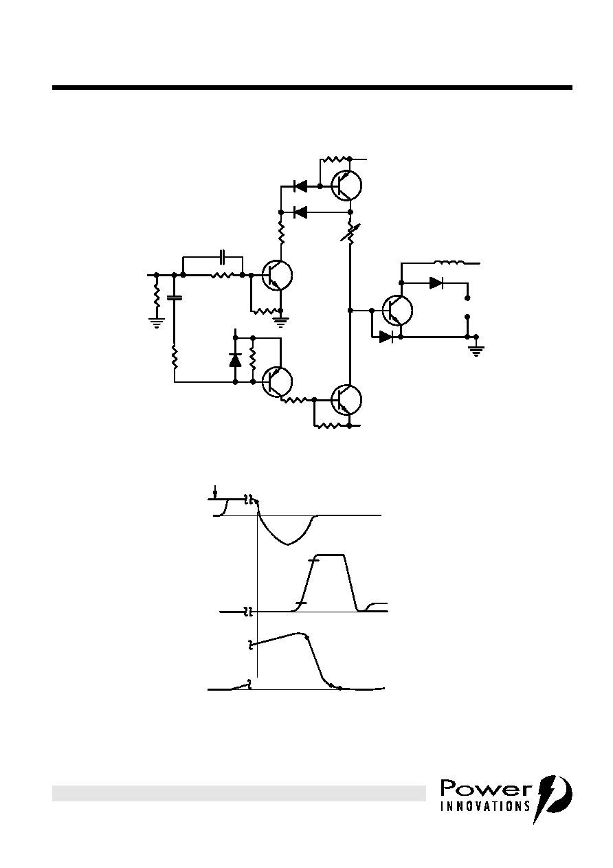
PARAMETER MEASUREMENT INFORMATION
Figure 1. Inductive-Load Switching Test Circuit
Figure 2. Inductive-Load Switching Waveforms
RB
(on)
V
BE(off)
Vclamp = 400 V
vcc
µ
µ
H
180
33
+5V
D45H11
BY205-400
BY205-400
2N2222
BY205-400
5X BY205-400
BY205-400
1 k
68
1 k
47
2N2904
D44H11
100
270
V Gen
+5V
1 k
0.02
µ
µ
F
TUT
1 pF
33
Adjust pw to obtain I
C
For I
C
< 6 A V
CC
= 50 V
For I
C
6 A V
CC
= 100 V
Base Current
A (90%)
I
B(on)
IB
Collector Voltage
Collector Current
D (90%)
E (10%)
F (2%)
C
B
90%
10%
V
CE
I
C(on)
A - B = t
sv
B - C = t
rv
D - E = t
fi
E - F = t
ti
B - E = t
xo
NOTES: A. Waveforms are monitored on an oscilloscope with the following characteristics: t
r
< 15 ns, R
in
> 10
, C
in
< 11.5 pF.
B. Resistors must be noninductive types.
TIPL761B, TIPL761C
NPN SILICON POWER TRANSISTORS
4
MAY 1989 - REVISED MARCH 1997
P R O D U C T I N F O R M A T I O N
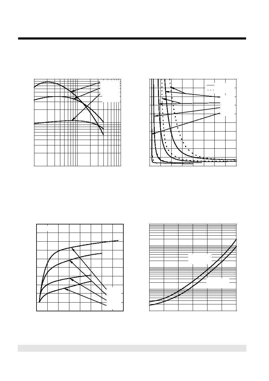
TYPICAL CHARACTERISTICS
Figure 3.
Figure 4.
Figure 5.
Figure 6.
TYPICAL DC CURRENT GAIN
vs
COLLECTOR CURRENT
I
C
- Collector Current - A
0∑1
1∑0
10
h
FE
- Typical DC Current Gain
1∑0
10
100
TCP741AA
V
CE
= 5 V
T
C
= 125∞C
T
C
= 25∞C
T
C
= -65∞C
COLLECTOR-EMITTER SATURATION VOLTAGE
vs
BASE CURRENT
I
B
- Base Current - A
0
0∑5
1∑0
1∑5
2∑0
V
CE(sat)
- Collector-Emitter Saturation Voltage - V
0
1∑0
2∑0
3∑0
4∑0
5∑0
TCP741AB
T
C
= 25∞C
T
C
= 100∞C
I
C
= 4 A
I
C
= 3 A
I
C
= 2 A
I
C
= 1 A
BASE-EMITTER SATURATION VOLTAGE
vs
BASE CURRENT
I
B
- Base Current - A
0
0∑2
0∑4
0∑6
0∑8
1∑0
1∑2
1∑4
1∑6
V
BE(sat)
- Base-Emitter Saturation Voltage - V
0∑75
0∑85
0∑95
1∑05
1∑15
1∑25
TCP741AC
T
C
= 25∞C
I
C
= 4 A
I
C
= 3 A
I
C
= 2 A
I
C
= 1 A
COLLECTOR CUT-OFF CURRENT
vs
CASE TEMPERATURE
T
C
- Case Temperature - ∞C
-60
-30
0
30
60
90
120
I
CES
- Collector Cut-off Current - µA
0∑001
0∑01
0∑1
1∑0
10
TCP741AN
TIPL761C
V
CE
= 1200 V
TIPL761B
V
CE
= 1100 V

5
MAY 1989 - REVISED MARCH 1997
TIPL761B, TIPL761C
NPN SILICON POWER TRANSISTORS
P R O D U C T I N F O R M A T I O N
MAXIMUM SAFE OPERATING REGIONS
Figure 7.
THERMAL INFORMATION
Figure 8.
MAXIMUM FORWARD-BIAS
SAFE OPERATING AREA
V
CE
- Collector-Emitter Voltage - V
1∑0
10
100
1000
I
C
- Collector Current - A
0∑01
0.1
1∑0
10
SAP741AC
t
p
= 10
µ
µ
s
t
p
= 100
µ
µ
s
t
p
= 1 ms
t
p
= 10 ms
DC Operation
TIPL761B
TIPL761C
THERMAL RESPONSE JUNCTION TO CASE
vs
POWER PULSE DURATION
t1 - Power Pulse Duration - s
10
-5
10
-4
10
-3
10
-2
10
-1
10
0
Z
JC
/R
JC
- Normalised Transient Thermal Impedance
0∑01
0∑1
1∑0
TCP741AE
t1
t2
duty cycle = t1/t2
Read time at end of t1,
T
J(max)
- T
C
= P
D(peak)
∑
∑ R
JC(max)
Z
JC
R
JC
( )
5%
10%
20%
50%
0%
TIPL761B, TIPL761C
NPN SILICON POWER TRANSISTORS
6
MAY 1989 - REVISED MARCH 1997
P R O D U C T I N F O R M A T I O N
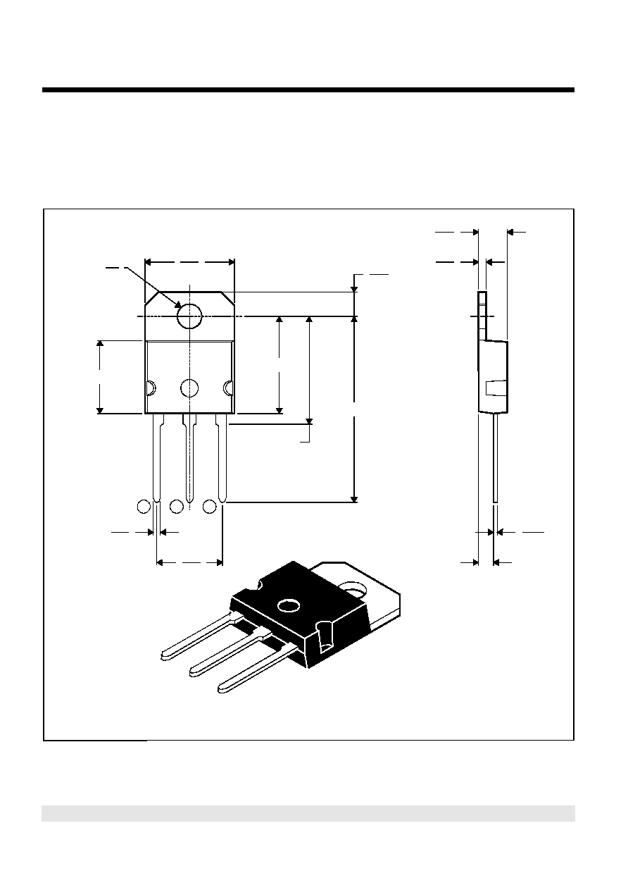
SOT-93
3-pin plastic flange-mount package
This single-in-line package consists of a circuit mounted on a lead frame and encapsulated within a plastic
compound. The compound will withstand soldering temperature with no deformation, and circuit performance
characteristics will remain stable when operated in high humidity conditions. Leads require no additional
cleaning or processing when used in soldered assembly.
MECHANICAL DATA
SOT-93
ALL LINEAR DIMENSIONS IN MILLIMETERS
4,90
4,70
1,37
1,17
0,78
0,50
2,50 TYP.
15,2
14,7
12,2 MAX.
16,2 MAX.
18,0 TYP.
31,0 TYP.
1,30
1,10
11,1
10,8
4,1
4,0
3,95
4,15
1
2
3
NOTE A: The centre pin is in electrical contact with the mounting tab.
MDXXAW
¯

7
MAY 1989 - REVISED MARCH 1997
TIPL761B, TIPL761C
NPN SILICON POWER TRANSISTORS
P R O D U C T I N F O R M A T I O N
IMPORTANT NOTICE
Power Innovations Limited (PI) reserves the right to make changes to its products or to discontinue any
semiconductor product or service without notice, and advises its customers to verify, before placing orders, that the
information being relied on is current.
PI warrants performance of its semiconductor products to the specifications applicable at the time of sale in
accordance with PI's standard warranty. Testing and other quality control techniques are utilized to the extent PI
deems necessary to support this warranty. Specific testing of all parameters of each device is not necessarily
performed, except as mandated by government requirements.
PI accepts no liability for applications assistance, customer product design, software performance, or infringement
of patents or services described herein. Nor is any license, either express or implied, granted under any patent
right, copyright, design right, or other intellectual property right of PI covering or relating to any combination,
machine, or process in which such semiconductor products or services might be or are used.
PI SEMICONDUCTOR PRODUCTS ARE NOT DESIGNED, INTENDED, AUTHORIZED, OR WARRANTED TO BE
SUITABLE FOR USE IN LIFE-SUPPORT APPLICATIONS, DEVICES OR SYSTEMS.
Copyright © 1997, Power Innovations Limited