 | –≠–ª–µ–∫—Ç—Ä–æ–Ω–Ω—ã–π –∫–æ–º–ø–æ–Ω–µ–Ω—Ç: TIPP32 | –°–∫–∞—á–∞—Ç—å:  PDF PDF  ZIP ZIP |

TIPP32, TIPP32A,TIPP32B, TIPP32C
PNP SILICON POWER TRANSISTORS
P R O D U C T I N F O R M A T I O N
1
MAY 1989 - REVISED MARCH 1997
Copyright © 1997, Power Innovations Limited, UK
Information is current as of publication date. Products conform to specifications in accordance
with the terms of Power Innovations standard warranty. Production processing does not
necessarily include testing of all parameters.
q
20 W Pulsed Power Dissipation
q
100 V Capability
q
2 A Continuous Collector Current
q
4 A Peak Collector Current
q
Customer-Specified Selections Available
LP PACKAGE
(TOP VIEW)
MDTRAB
E
C
B
1
2
3
absolute maximum ratings
at 25∞C case temperature (unless otherwise noted)
NOTES: 1. This value applies for t
p
0.3 ms, duty cycle
10%.
2. Derate linearly to 150∞C case temperature at the rate of 6.4 mW/∞C.
3. V
CE
= 20 V, I
C
= 1 A, t
p
= 10 ms, duty cycle
2%.
RATING
SYMBOL
VALUE
UNIT
Collector-base voltage (I
E
= 0)
TIPP32
TIPP32A
TIPP32B
TIPP32C
V
CBO
-40
-60
-80
-100
V
Collector-emitter voltage (I
B
= 0)
TIPP32
TIPP32A
TIPP32B
TIPP32C
V
CEO
-40
-60
-80
-100
V
Emitter-base voltage
V
EBO
-5
V
Continuous collector current
I
C
-2
A
Peak collector current (see Note 1)
I
CM
-4
A
Continuous base current
I
B
-1
A
Continuous device dissipation at (or below) 25∞C case temperature (see Note 2)
P
tot
0.8
W
Pulsed power dissipation (see Note 3)
P
T
20
W
Operating junction temperature range
T
j
-55 to +150
∞C
Storage temperature range
T
stg
-55 to +150
∞C
Lead temperature 3.2 mm from case for 10 seconds
T
L
260
∞C

TIPP32, TIPP32A,TIPP32B, TIPP32C
PNP SILICON POWER TRANSISTORS
2
MAY 1989 - REVISED MARCH 1997
P R O D U C T I N F O R M A T I O N
NOTES: 4. These parameters must be measured using pulse techniques, t
p
= 300 µs, duty cycle
2%.
5. These parameters must be measured using voltage-sensing contacts, separate from the current carrying contacts.
electrical characteristics at 25∞C case temperature
PARAMETER
TEST CONDITIONS
MIN
TYP
MAX
UNIT
V
(BR)CEO
Collector-emitter
breakdown voltage
I
C
= -5 mA
(see Note 4)
I
B
= 0
TIPP32
TIPP32A
TIPP32B
TIPP32C
-40
-60
-80
-100
V
I
CES
Collector-emitter
cut-off current
V
CE
= -40 V
V
CE
= -60 V
V
CE
= -80 V
V
CE
= -100 V
V
BE
= 0
V
BE
= 0
V
BE
= 0
V
BE
= 0
TIPP32
TIPP32A
TIPP32B
TIPP32C
-0.2
-0.2
-0.2
-0.2
mA
I
CEO
Collector cut-off
current
V
CE
= -30 V
V
CE
= -60 V
I
B
= 0
I
B
= 0
TIPP32/32A
TIPP32B/32C
-0.3
-0.3
mA
I
EBO
Emitter cut-off
current
V
EB
= -5 V
I
C
= 0
-1
mA
h
FE
Forward current
transfer ratio
V
CE
= -4 V
V
CE
= -4 V
I
C
= -1 A
I
C
= -2 A
(see Notes 4 and 5)
20
10
V
CE(sat)
Collector-emitter
saturation voltage
I
B
= -375 mA
I
C
= -2 A
(see Notes 4 and 5)
-1
V
V
BE
Base-emitter
voltage
V
CE
= -4 V
I
C
= -2 A
(see Notes 4 and 5)
-1.5
V
h
fe
Small signal forward
current transfer ratio
V
CE
= -10 V
I
C
= -0.5 A
f = 1 kHz
20
|
h
fe
|
Small signal forward
current transfer ratio
V
CE
= -10 V
I
C
= -0.5 A
f = 1 MHz
3
3
MAY 1989 - REVISED MARCH 1997
TIPP32, TIPP32A,TIPP32B, TIPP32C
PNP SILICON POWER TRANSISTORS
P R O D U C T I N F O R M A T I O N
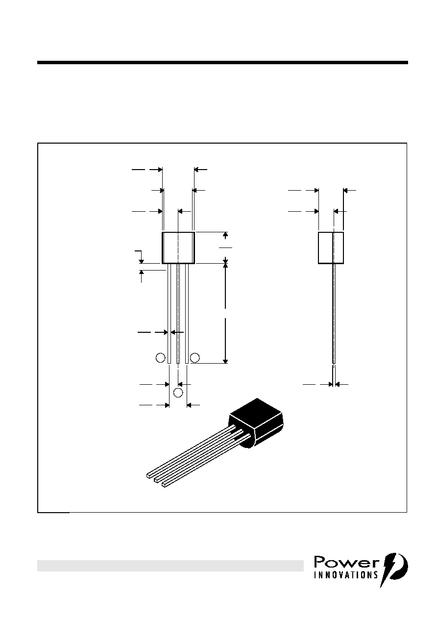
LP003 (TO-92)
3-pin cylindical plastic package
This single-in-line package consists of a circuit mounted on a lead frame and encapsulated within a plastic
compound. The compound will withstand soldering temperature with no deformation, and circuit performance
characteristics will remain stable when operated in high humidity conditions. Leads require no additional
cleaning or processing when used in soldered assembly.
MECHANICAL DATA
ALL LINEAR DIMENSIONS IN MILLIMETERS
12,7 MIN.
2,03
2,67
4,44
5,21
3,43 MIN.
4,32
5,34
0,40
0,56
1,14
1,40
2,41
2,67
0,35
0,41
2,03
2,67
3,17
4,19
(see Note A)
Seating Plane
1
2
3
LP003 (TO-92)
LP003 Falls Within JEDEC
TO-226AA Dimensions
MDXXAX
1,27
NOTE A: Lead dimensions are not controlled in this area.
TIPP32, TIPP32A,TIPP32B, TIPP32C
PNP SILICON POWER TRANSISTORS
4
MAY 1989 - REVISED MARCH 1997
P R O D U C T I N F O R M A T I O N
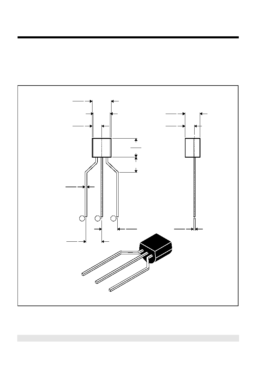
LP003 (TO-92)
3-pin cylindical plastic package
This single-in-line package consists of a circuit mounted on a lead frame and encapsulated within a plastic
compound. The compound will withstand soldering temperature with no deformation, and circuit performance
characteristics will remain stable when operated in high humidity conditions. Leads require no additional
cleaning or processing when used in soldered assembly.
MECHANICAL DATA
LP003 (TO-92) - Formed Leads Version
ALL LINEAR DIMENSIONS IN MILLIMETERS
2,03
2,67
4,44
5,21
3,43 MIN.
4,32
5,34
0,40
0,56
2,40
2,90
0,35
0,41
2,03
2,67
3,17
4,19
4,00 MAX.
2,90
2,40
LP003 Falls Within JEDEC
TO-226AA Dimensions
1
2
3
MDXXAR

5
MAY 1989 - REVISED MARCH 1997
TIPP32, TIPP32A,TIPP32B, TIPP32C
PNP SILICON POWER TRANSISTORS
P R O D U C T I N F O R M A T I O N
LPR
tape dimensions
MECHANICAL DATA
LP Package (TO-92) Tape (Formed Lead Version)
ALL LINEAR DIMENSIONS IN MILLIMETERS
0,00
0,50
5,50
19,00
8,50
9,75
17,50
19,00
¯
3,70
4,30
12,40
13,00
5,95
6,75
2,40
2,90
8,50
11,00
15,50
16,50
17,66
27,68
23,00
32,00
11,70
13,70
2,50 MIN.
2,90
2,40
4,44
5,21
2,03
2,67
3,43 MIN.
4,32
5,34
4,00 MAX.
0,40
0,56
3,17
4,19
2,03
2,67
0,35
0,41
MDXXAS

TIPP32, TIPP32A,TIPP32B, TIPP32C
PNP SILICON POWER TRANSISTORS
6
MAY 1989 - REVISED MARCH 1997
P R O D U C T I N F O R M A T I O N
IMPORTANT NOTICE
Power Innovations Limited (PI) reserves the right to make changes to its products or to discontinue any
semiconductor product or service without notice, and advises its customers to verify, before placing orders, that the
information being relied on is current.
PI warrants performance of its semiconductor products to the specifications applicable at the time of sale in
accordance with PI's standard warranty. Testing and other quality control techniques are utilized to the extent PI
deems necessary to support this warranty. Specific testing of all parameters of each device is not necessarily
performed, except as mandated by government requirements.
PI accepts no liability for applications assistance, customer product design, software performance, or infringement
of patents or services described herein. Nor is any license, either express or implied, granted under any patent
right, copyright, design right, or other intellectual property right of PI covering or relating to any combination,
machine, or process in which such semiconductor products or services might be or are used.
PI SEMICONDUCTOR PRODUCTS ARE NOT DESIGNED, INTENDED, AUTHORIZED, OR WARRANTED TO BE
SUITABLE FOR USE IN LIFE-SUPPORT APPLICATIONS, DEVICES OR SYSTEMS.
Copyright © 1997, Power Innovations Limited